red
The Fourth Element: Characteristics, Modelling, and Electromagnetic Theory of the Memristor
Abstract
Memristor, SPICE macro-model, Nonlinear circuit theory, Nonvolatile memory, Dynamic systems In 2008, researchers at HP Labs published a paper in Nature reporting the realisation of a new basic circuit element that completes the missing link between charge and flux-linkage, which was postulated by Leon Chua in 1971. The HP memristor is based on a nanometer scale TiO2 thin-film, containing a doped region and an undoped region. Further to proposed applications of memristors in artificial biological systems and nonvolatile RAM (NVRAM), they also enable reconfigurable nanoelectronics. Moreover, memristors provide new paradigms in application specific integrated circuits (ASICs) and field programmable gate arrays (FPGAs). A significant reduction in area with an unprecedented memory capacity and device density are the potential advantages of memristors for Integrated Circuits (ICs). This work reviews the memristor and provides mathematical and SPICE models for memristors. Insight into the memristor device is given via recalling the quasi-static expansion of Maxwell’s equations. We also review Chua’s arguments based on electromagnetic theory.
1 Introduction
Based on the International Technology Roadmap for Semiconductors (ITRS) report (ITRS, 2007), it is predicted that by 2019, half-pitch Dynamic Random Access Memory (DRAM) cells will provide a capacity around , assuming area efficiency. Interestingly, memristors promise extremely high capacity more than and for and half-pitch devices, respectively (Williams, 2008; Lewis and Lee, 2009). In contrast to DRAM memory, memristors provide nonvolatile operation as is the case for flash memories. Hence, such devices can continue the legacy of Moore’s law for another decade. Furthermore, inclusion of molecular electronics and computing as an alternative to CMOS technologies in the recent ITRS report emphasises the significant challenges of device scaling (Jones, 2009). Moreover, Swaroop et al. (1998) demonstrated that the complexity of a synapse, in an analog VLSI neural network implementation, is minimised by using a device called the Programmable Metallization Cell (PMC). This is an ionic programmable resistive device and a memristor can be employed to play the same role.
Research on memristor applications in various areas of circuit design, alternative materials and spintronic memristors, and especially memristor device/circuit modeling have appeared in the recent literature, (i) SPICE macro-modeling using linear and non-linear drift models (Chen and Wang, 2009; Zhang et al., 2009; Biolek et al., 2009b; Benderli and Wey, 2009; Kavehei et al., 2009; Wang et al., 2009a), (ii) Application of memristors in different circuit configurations and their dynamic behaviour (Li et al., 2009; Sun et al., 2009b; Wang et al., 2009b; Sun et al., 2009a), (iii) Application of memristor based dynamic systems to image encryption in Lin and Wang (2009), (iv) Fine resolution programmable resistor using a memristor in Shin et al. (2009), (v) Memristor-based op-amp circuit and filter characteristics of memristors by Yu et al. (2009) and Wang et al. (2009c), respectively, (vi) Memristor receiver (MRX) structure for ultra-wide band (UWB) wireless systems (Itoh and Chua, 2008; Witrisal, 2009), (vii) Memristive system I/O nonlinearity cancellation in Delgado (2009), (viii) The number of required memristors to compute a function by Lehtonen and Laiho (2009), and its digital logic implementation using a memristor-based crossbar architecture in Raja and Mourad (2009), (ix) Different physical mechanisms to store information in memristors (Driscoll et al., 2009; Wang et al., 2009d), (x) Interesting fabricated nonvolatile memory using a flexible memristor, which is an inexpensive and low-power device solution is also recently reported (Gergel-Hackett et al., 2009), (xi) Using the memductance concept to develop an equivalent circuit diagram of a transmission-line has been carried out by Mallégol (2003, appendix 2).
There are still many problems associated with memristor device level. For instance, it is not clear that which leakage mechanisms are associated with the device. The flexible memristor is able to retain its nonvolatile characteristic for up to 14 days or, equivalently, up to 4000 flexes (Gergel-Hackett et al., 2009). Thus, the nonvolatility feature eventually vanishes after a short period. Strukov and Williams (2009) also investigated this particular feature as a ratio of volatility to switching time.
One disadvantage of using memristors is switching speed. The volatility-to-switching speed ratio for memristor cells, in the HP cross-bar structure is around (Strukov and Williams, 2009), which is much lower than the ratio for DRAM cells, (ITRS, 2007), therefore, the switching speed of memristors is far behind DRAM. However, unlike DRAM, RRAM is non-volatile. In terms of yield, DRAM and RRAM are almost equal (Lewis and Lee, 2009). Generally, endurance becomes very important once we note that the DRAM cells must be refreshed at least every , which means at least write cycles in their life time (Lewis and Lee, 2009). Unfortunately, memristors are far behind DRAM in terms of the endurance view point, but the HP team is confident that there is no functional limitation against improvement of memristor (Williams, 2008). Finally, another advantage of RRAM is readability. Readability refers to the ability of a memory cell to report its state. This noise immunity in DRAM is weak because each DRAM cell stores a very small amount of charge particularly at nanometer dimensions, while in RRAM cells, e.g. memristors, it depends on the difference between the on and off state resistances (Lewis and Lee, 2009). This difference was reported up to one order of magnitude (Williams, 2008).
It is interesting to note that there are devices with similar behaviour to a memristor, e.g. (Buot and Rajagopal, 1994; Beck et al., 2000; Krieger et al., 2001; Liu et al., 2006; Waser and Masakazu, 2007; Ignatiev et al., 2008; Tulina et al., 2008), but the HP scientists were the only group that found the link between their work and the missing memristor postulated by Chua. Moreover, it should be noted that physically realised memristors must meet the mathematical requirements of a memristor device or memristive systems that are discussed in Kang (1975) and Chua and Kang (1976). For instance, the hysteresis loop must have a double-valued bow-tie trajectory. However, for example in Krieger et al. (2001), the hysteresis loop shows more than two values for some applied voltage values. Beck et al. (2000) demonstrates one of the perfect examples of memristor devices. Kim et al. (2009a) recently introduced a multilevel one-time programmable (OTP) oxide diode for crossbar memories. They focused on a one-time programmable structure that basically utilises one diode and one resistor, 1D-1R, since obtaining a stable device for handling multiple programming and erasing processes is much more difficult than a one-time programmable device. In terms of functionality, OTP devices are very similar to memristive elements, but in terms of flexibility, memristors are able to handle multiple programming and erasing processes.
This paper focuses on the memristor device and reviews its device level properties. Although the memristor as a device is new, it was conceptually postulated by Chua (1971). Chua predicted that a memristor could be realised as a purely dissipative device as a fourth fundamental circuit element. Thirty seven years later, Stan Williams and his group in the Information and Quantum Systems (IQS) Lab at HP realised the memristor in device form (Strukov et al., 2008).
In Section 2, we review the memristor and its characteristics as a nano-switch, which was realised by Hewlett-Packard (HP) (Strukov et al., 2008), and we review its properties based on the early mathematical models. We introduce a new model using a parameter we call the resistor modulation index (RMI). Due to the significance of ionic drift that plays the most important role in the memristive effect, this section is divided into two: (2.1) a linear, and (2.2) a nonlinear drift model. Section 3 presents a preliminary SPICE macro-model of the memristor and different types of circuit elements in combination with a proposed memristor macro-model. Section 4 describes an interpretation of the memristor based on electromagnetic theory by recalling Maxwell’s equations. Finally, we summarise this review in Section 5.
2 Memristor Device Properties
Traditionally there are only three fundamental passive circuit elements: capacitors, resistors, and inductors, discovered in 1745, 1827, and 1831, respectively. However, one can set up five different mathematical relations between the four fundamental circuit variables: electric current , voltage , electric charge , and magnetic flux . For linear elements, , where (), and where (), indicate linear resistors, capacitors, and inductors, respectively.
In 1971, Leon Chua, proposed that there should be a fourth fundamental passive circuit element to set up a mathematical relationship between and , which he named the memristor (a portmanteau of memory and resistor) (Chua, 1971). Chua predicted that a class of memristors might be realisable in the form of a pure solid-state device without an internal power supply.
In 2008, Williams et al., at Hewlett Packard, announced the first fabricated memristor device (Strukov et al., 2008). However, a resistor with memory is not a new thing. If taking the example of nonvolatile memory, it dates back to 1960 when Bernard Widrow introduced a new circuit element named the memistor (Widrow et al., 1960). The reason for choosing the name of memistor is exactly the same as the memristor, a resistor with memory. The memistor has three terminals and its resistance is controlled by the time integral of a control current signal. This means that the resistance of the memistor is controlled by charge. Widrow devised the memistor as an electrolytic memory element to form a basic structure for a neural circuit architecture called ADALINE (ADAptive LInear NEuron), which was introduced by him and his postgraduate student, Marcian Edward “Ted” Hoff (Widrow et al., 1960). However, the memistor is not exactly what researchers were seeking at the nanoscale. It is just a charge-controlled three-terminal (transistor) device. In addition, a two-terminal nano-device can be fabricated without nanoscale alignment, which is an advantage over three-terminal nano-devices (Lehtonen and Laiho, 2009). Furthermore, the electrochemical memistors could not meet the requirement for the emerging trend of solid-state integrated circuitry.
Thirty years later, Thakoor et al. (1990) introduced a solid-state thin-film tungsten-oxide-based, nonvolatile memory. The concept is almost similar to the HP memristors. Their solid-state memistor is electrically reprogrammable, it has variable resistance, and it is an analog synaptic memory connection that can be used in electrical neural networks. They claimed that the resistance of the device could be stabilised at any value, between and . This solid-state memistor has a thick, -, layer of silicon dioxide that achieves nonvolatility over a period of several months. This thick electron blocking layer, however, causes a considerable reduction in the applied electric field. As a consequence, they reported very high programming voltages ( 25 to 30 ) and very long (minutes to hours) switching times.
In the 1960s, the very first report on the hysteresis behaviour of current-voltage curve was published by Simmons (1963), which is known as the Simmons tunneling theory. The Simmons theory generally characterises the tunneling current in a Metal-Insulator-Metal (MIM) system. A variable resistance with hysteresis was also published by Simmons and Verderber (1967). They introduced a thin-film ( to ) silicon dioxide doped with gold ions sandwiched between two metal contacts. Thus overall the device is a MIM system, using aluminum metal contacts. Interestingly, their system demonstrates a sinh function behaviour as also recently reported in Yang et al. (2008) for the HP memristor. It is also reported that the switching from high- to low impedance takes about . As their device is modelled as an energy storage element it cannot be a memristor, because memristors remember the total charge passing through the port and do not store charge (Oster, 1974).
The sinh resistance behaviour of memristors can be utilised to compensate the linearity of analog circuits. In Varghese and Gandhi (2009) a memristor based amplifier was proposed utilising the behaviour of a sinh resistor (Tavakoli and Sarpeshkar, 2005) as a memristor element. In Shin et al. (2009) such a structure was also introduced as an example without mentioning the sinh resistance behaviour of memristors. The idea in Tavakoli and Sarpeshkar (2005) is to characterise a sinh function type circuit that can be used to linearise a tanh function type circuit behaviour, e.g. CMOS differential amplifier. A theoretical analysis shows that a sinh function significantly reduces the third harmonic coefficient and as a consequence reduces nonlinearity of circuit.
Chua mathematically predicted that there is a solid-state device, which defines the missing relationship between four basic variables (Chua, 1971). Recall that a resistor establishes a relation between voltage and current, a capacitor establishes a charge-voltage relation, and an inductor realises a current-flux relationship, as illustrated in Fig. 1. Notice that we are specifically discussing nonlinear circuit elements here.
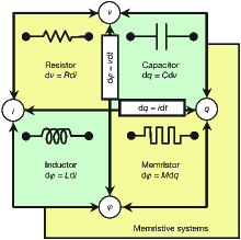
Consequently, or defines a charge-controlled (flux-controlled) memristor. Then, or , which implies or . Note that, for a charge-controlled memristor and for a flux-controlled memristor, where is the incremental memristance and is the incremental memductance where is in the units of Ohms and the units of is in Siemens (Chua, 1971).
Memristance, , is the slope of the - curve, which for a simple case, is a piecewise - curve with two different slopes. Thus, there are two different values for , which is exactly what is needed in binary logic. For detailed information regarding typical - curves, the reader is referred to Chua (1971).
It is also obvious that if , then instantaneous power dissipated by a memristor, , is always positive so the memristor is a passive device. Thus the - curve is a monotonically-increasing function. This feature is exactly what is observed in the HP memristor device (Strukov et al., 2008). Some other properties of the memristor such as zero-crossing between current and voltage signals can be found in Chua (1971) and Chua and Kang (1976). The most important feature of a memristor is its pinched hysteresis loop - characteristic (Chua and Kang, 1976). A very simple consequence of this property and is that such a device is purely dissipative like a resistor.
Another important property of a memristor is its excitation frequency. It has been shown that the pinched hysteresis loop is shrunk by increasing the excitation frequency (Chua and Kang, 1976). In fact, when the frequency increases toward infinity, the memristor acts as a linear resistor (Chua and Kang, 1976).
Interestingly enough, an attractive property of the HP memristor (Strukov et al., 2008), which is exclusively based on its fabrication process, can be deduced from the HP memristor simple mathematical model (Strukov et al., 2008) and is given by,
| (1) |
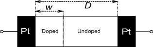
where has the dimensions of magnetic flux . Here, in units of , where is the average drift mobility in unit of and is the film (titanium dioxide, TiO2) thickness. Note that and are simply the ‘on’ and ‘off’ state resistances as indicated in Fig. 2. Also defines the total charge passing through the memristor device in a time window, - . Notice that the memristor has an internal state (Chua and Kang, 1976). Furthermore, as stated in Oster (1974), , as the state variable in a charge-controlled memristor gives the charge passing through the device and does not behave as storage charge as in a capacitor as incorrectly reported in some works, e.g. Simmons and Verderber (1967). This concept is very important from two points of view. First of all, a memristor is not an energy-storage element. Second, this shows that the memristor is not merely a nonlinear resistor, but is a nonlinear resistor with charge as a state variable (Oster, 1974).
Five years after Chua’s paper on the memristor (Chua, 1971), he and his graduate student, Kang, published a paper defining a much broader class of systems, named memristive systems. From the memristive systems viewpoint a generalized definition of a memristor is , where defines the internal state of the system and (Chua and Kang, 1976). Based on this definition a memristor is a special case of a memristive system.
The HP memristor (Strukov et al., 2008) can be defined in terms of memristive systems. It exploits a very thin-film TiO2 sandwiched between two platinum (Pt) contacts and one side of the TiO2 is doped with oxygen vacancies, which are positively charged ions. Therefore, there is a TiO2 junction where one side is doped and the other is undoped. Such a doping process results in two different resistances: one is a high resistance (undoped) and the other is a low resistance (doped). Hence, HP intentionally established a device that is illustrated in Fig. 2. The internal state variable, , is also the variable length of the doped region. Roughly speaking, when we have nonconductive channel and when we have conductive channel. The HP memristor switching mechanism is further discussed in Yang et al. (2008).
2.1 Linear drift model
The memristor’s state equation is at the heart of the HP memristive system mechanism (Wang, 2008; Joglekar and Wolf, 2009). Let us assume a uniform electric field across the device, thus there is a linear relationship between drift-diffusion velocity and the net electric field (Blanc and Staebler, 1971). Therefore the state equation is,
| (2) |
Integrating Eq. 2 gives , where is the initial length of . Hence, the speed of drift under a uniform electric field across the device is given by . In a uniform field we have . In this case also defines the amount of required charge to move the boundary from , where , to distance , where . Therefore, , so
| (3) |
If then
| (4) |
where describes the amount of charge that is passed through the channel over the required charge for a conductive channel.
Using Strukov et al. (2008) we have,
| (5) |
By inserting , Eq. 5 can be rewritten as
| (6) |
Now assume that then , and from Eq. 6,
| (7) |
where and is the memristance value at . Consequently, the following equation gives the memristance at time ,
| (8) |
Substituting Eq. 8 into , when , we have,
| (9) |
Recalling that , the solution is
| (10) |
Using , Eq. 10 becomes,
| (11) |
Consequently, using Eq. 4 if , so the internal state of the memristor is
| (12) |
The current-voltage relationship in this case is,
| (13) |
In Eq. 13, the inverse square relationship between memristance and TiO2 thickness, , shows that for smaller values of , the memristance shows improved characteristics, and because of this reason the memristor imposes a small value of .
In Eqs. 10-13, the only term that significantly increases the role of is lower . This shows that at the micrometer scale is negligible and the relationship between current and voltage reduces to a resistor equation.
Substituting that has the same units as magnetic flux into Eq. 13, and considering as a normalised variable, we obtain
| (14) |
where is what we call the resistance modulation index, (RMI) (Kavehei et al., 2009).
Due to the extremely uncertain nature of nanotechnologies, a variability-aware modeling approach should be always considered. Two well-know solutions to analyse a memristive system were investigated in Chen and Wang (2009), 1) Monte-Carlo simulation for evaluating (almost) complete statistical behaviour of device, and 2) Corner analysis. Considering the trade-off between time-complexity and accuracy between these two approach as shows the importance of using a simple and reasonably accurate model, because finding the real corners is highly dependent on the model accuracy. The resistance modulation index, RMI, could be one of the device parameters in the model extraction phase, so it would help to provide a simple model with fewer parameters.
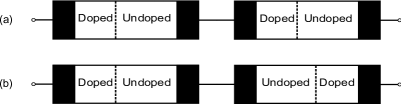
Joglekar and Wolf (2009) clarified the behaviour of two memristors in series. As shown in Fig. 3, they labeled the polarity of a memristor by , where signifies that increases with positive voltage or, in other words, the doped region in memristor is expanding. If the doped region, , is shrinking with positive voltage, then . In other words, reversing the voltage source terminals implies memristor polarity switching. In Fig. 3 (a), the doped regions are simultaneously shrunk so the overall memristive effect is retained. In Fig. 3 (b), however, the overall memristive effect is suppressed (Joglekar and Wolf, 2009).
Using the memristor polarity effect and Eq. 2, we thus obtain
| (15) |
Then with similar approach we have
| (16) |
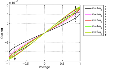
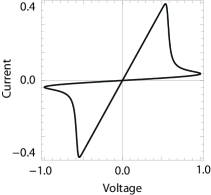
There is also no phase shift between current and voltage signals, which implies that the hysteresis loop always crosses the origin as demonstrated in Fig. 4. For further investigation, if a voltage, , is applied across the device, the magnetic flux would be . The inverse relation between flux and frequency shows that at very high frequencies there is only a linear resistor.
Fig. 4 demonstrates Eq. 16 in MATLAB for five different frequencies, where , using the Strukov et al. (2008) parameter values, , , , , , and . The resistance modulation index, simulation with the same parameter values is shown in Fig. 5.
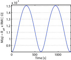
Using different parameters causes a large difference in the hysteresis and memristor characteristics. In Witrisal (2009), a new solution for ultra-wideband signals using memristor devices was introduced. Applying the parameter values given in Witrisal (2009) results in a significant difference in the value of . Substituting parameter values given in the paper gives instead of , using to and the parameter values from Strukov et al. (2008). The new parameter values are , , , , and . Using these parameters shows that even though the highest and lowest memristance ratio in the last case, Fig. 4, is around , here the ratio is approximately equal to .
2.2 Nonlinear drift model
The electrical behaviour of the memristor is directly related to the shift in the boundary between doped and undoped regions, and the effectively variable total resistance of the device when an electrical field is applied. Basically, a few volts supply voltage across a very thin-film, e.g. , causing a large electric field. For instance, it could be more than , which results in a fast and significant reduction in energy barrier (Blanc and Staebler, 1971). Therefore, it is reasonable to expect a high nonlinearity in ionic drift-diffusion (Waser et al., 2009).
One significant problem with the linear drift assumption is the boundaries. The linear drift model, Eq. 2, suffers from problematic boundary effects. Basically, at the nanoscale, a few volts causes a large electric field that leads to a significant nonlinearity in ionic transport (Strukov et al., 2008). A few attempts have been carried out so far to consider this nonlinearity in the state equation (Strukov et al., 2008; Strukov and Williams, 2009; Biolek et al., 2009b; Benderli and Wey, 2009). All of them proposed a simple window function, , which is multiplied by the right-hand side of Eq. 2. In general, could be a variable vector, e.g. where and are the memristor’s state variable and current, respectively.
In general, the window function can be multiplied by the right-hand side of the state variable equation, Eq. 2,
| (17) |
where is the normalised form of the state variable. The window function makes a large difference between the model with linear and nonlinear drift assumptions at the boundaries. Fig. 6 shows such a condition considering a nonlinear drift assumption at the critical, or boundary, states. In other words, when a linear drift model is used, simulations should consider the boundaries and all constraints on initial current, initial voltage, maximum and minimum , and etc. These constraints cause a large difference in output between linear and nonlinear drift assumptions. For example, it is impossible to achieve such a realistic curve, as in Fig. 6, using the linear drift modeling approach.
In Strukov et al. (2008), the window function is a function of the state variable and it is defined as . The boundary conditions in this case are and . It meets the essential boundary condition , except there is a slight difference when . The problem of this boundary assumption is when a memristor is driven to the terminal states, and , then , so no external field can change the memristor state (Biolek et al., 2009b). This is a fundamental problem of the window function. The second problem of the window function is it assumes that the memristor remembers the amount of charge that passed through the device. Basically, this is a direct result of the state equation, Eq. 2, (Biolek et al., 2009b). However, it seems that the device remembers the position of boundary between the two regions, and not the amount of charge.
In Benderli and Wey (2009), another window function has been proposed that is slightly different from that in Strukov et al. (2008). This window function, , approaches zero when and when then . Therefore, this window function meets both the boundary conditions. In fact, the second window function is imitates the first function when we consider instead of . In addition, there is another problem associated with these two window functions, namely, the modeling of approximate linear ionic drift when . Both of the window functions approximate nonlinear behaviour when the memristor is not in its terminal states, or . This problem is addressed in Joglekar and Wolf (2009) where they propose an interesting window function to address the nonlinear and approximately linear ionic drift behaviour at the boundaries and when , respectively. Nonlinearity (or linearity) of their function can be controlled with a second parameter, which we call the control parameter, . Their window function is , where and is a positive integer. Fig. 7 (a) demonstrates the function behaviour for different values. This model considers a simple boundary condition, . As demonstrated, when , the state variable equation is an approximation of the linear drift assumption, .
The most important problem associated with this model is revealed at the boundaries. Based on this model, when a memristor is at the terminal states, no external stimulus can change its state. Biolek et al. (2009b) tackles this problem with a new window function that depends on , , and memristor current, . Basically, and are playing the same role in their model and the only new idea is using current as an extra parameter. The window function is, , where is memristor current and when , and when . As a matter of fact, when the current is positive, the doped region length, , is expanding. Fig. 7 (b) illustrates the window function behaviour.

All window functions suffer from a serious problem. They are only dependent on the state variable, , which implies that the memristor remembers the entire charge that is passing through it. Moreover, based on the general definition of the time-invariant memristor’s state equation and current-voltage relation, or , and must be continuous -dimensional vector functions (Kang, 1975, chap. 2). However, the last window function, , does not provide the continuity condition at the boundaries, or . Biolek et al. (2009b) did not use the window function in their recent publication (Biolek et al., 2009a).
In Strukov and Williams (2009) the overall drift velocity is identified with one linear equation and one highly nonlinear equation, , when and , for , where is the average drift velocity, is an applied electric field, is the mobility, and is the characteristic field for a particular mobile ion. The value of is typically about at room temperature (Strukov and Williams, 2009). This equation shows that a very high electric field is needed for exponential ion transport. They also showed that the high electric field is lower than the critical field for dielectric breakdown of the oxide. Reviewing the available window functions indicates that there is a need for an appropriate model that can define memristor states for strongly nonlinear behavior where, .
In addition to the weakness of nonlinear modeling in the original HP model, there are some other drawbacks that show the connection between physics and electronic behaviour was not well established. Moreover, the currently available electronic models for memristors followed the exact pathway of the HP modeling, which is mostly due to the fact that the underlying physical conduction mechanism is not fully clear yet (Kim et al., 2009b). One weakness is that the HP model does not deliver any insight about capacitive effects, which are naturally associated with memristors. These capacitive effects will later be explained in terms of a memcapacitive effect in a class of circuit elements with memory. In Kim et al. (2009b) the memristor behaviour was realised using infinite number of crystalline magnetite (Fe3O4) nanoparticles. The device behaviour combines both memristive (time-varying resistance) and memcapacitive (time-varying capacitance) effects, which deliver a better model for the nonlinear properties. Their model description for current-voltage relationship is given as,
| (18) |
where and are the time-varying resistance and capacitance effects, respectively. The time-dependent capacitor is a function of the state variable, and , where is defined as the additional capacitance caused by changing the value of capacitance (Kim et al., 2009b), , where is the capacitance at . The state variable is also given by,
| (19) |
Kim et al. (2009b) also investigated the impact of temperature variation on their Fe3O4 nanoparticle memristor assemblies of equal to , , and . It was reported that the change in electrical resistivity (specific electrical resistance), , as an explicit function of temperature can be defined by, , which means there is a significantly increasing behaviour as temperature decreases. As a consequence, for example, there is no hysteresis loop signature at room temperature, , () while at it shows a nice bow-tie trajectory. As they claimed, the first room temperature reversible switching behaviour was observed in their nanoparticle memristive system (Kim et al., 2009b).
It is worth noting that there are also two other elements with memory named the memcapacitor (Memcapacitive, MC, Systems) and meminductor (Meminductive, MI, Systems). Di Ventra et al. (2009) postulated that these two elements also could be someday realised in device form. The main difference between these three elements, the memristor, memcapacitor, and meminductor is that, the memristor is not a lossless memory device and dissipates energy as heat. However, at least in theory, the memcapacitor and meminductor are lossless devices because they do not have resistance. Di Ventra et al. (2009) also investigated some examples of using different nanoparticle-based thin-film materials. Memristors (Memresistive, MR, Systems) are identified by a hysteresis current-voltage characteristic, whereas MC and MI systems introduce Lissajous curves for charge-voltage and flux-current, respectively. Similar to memristors, there are two types of these elements, therefore, the three circuit elements with memory (mem-systems/devices) can be summarised as follows,
- Memristors
-
(MR Systems): A memristor is an one-port element whose instantaneous electric charge and flux-linkage, denoted by and , respectively, satisfy the relation . It has been proven that these devices are passive elements (Strukov et al., 2008). As discussed, they cannot store energy, so whenever and there is a pinched hysteresis loop between current and voltage. Thus, charge-flux curve is a monotonically-increasing function. A memristor acts as a linear resistor when frequency goes toward infinity and as a nonlinear resistor at low frequencies. Due to the nonlinear resistance effect, should be utilised instead of . There are two types of control process,
- I.
-
th order current-controlled MR systems 111Current- (and voltage-) controlled is a better definition for memristors because they do not store any charge (Oster, 1974). In Di Ventra et al. (2009) it is specified as current- (and voltage-) controlled instead of charge- (and flux-) controlled in Chua (1971)., ,
-
•
-
•
-
•
- II.
-
th order voltage-controlled MR systems, ,
-
•
-
•
.
-
•
- Memcapacitors
-
(MC Systems): A memcapacitor is an one-port element whose instantaneous flux-linkage and time-integral of electric charge, denoted by and , respectively, satisfy the relation . The total added/removed energy to/from a voltage-controlled MC system, , is equal to the linear summation of areas between - curve in the first and third quadrants with opposite signs. Due to the nonlinear capacitance effect, should be utilised instead of , so . In principle a memcapacitor can be a passive, an active, and even a dissipative222Adding energy to system. element (Di Ventra et al., 2009). If and capacitance is varying between two constant values, and , then the memcapacitor is a passive element. It is also important to note that, assuming zero charged initial state for a passive memcapacitor, the amount of removed energy cannot exceed the amount of previously added energy (Di Ventra et al., 2009). A memcapacitor acts as a linear capacitor when frequency tend to infinity and as a nonlinear capacitor at low frequencies. There are two types of control process,
- I.
-
th order voltage-controlled MC systems, ,
-
•
-
•
-
•
- II.
-
th order charge-controlled MC systems, ,
-
•
-
•
.
-
•
- Meminductors
-
(ML Systems): A meminductor is a one-port element whose instantaneous electric charge and time-integral of flux-linkage, denoted by and , respectively, satisfy the relation . In the total stored energy equation in a ML system, , the nonlinear inductive effect, should be taken into account. Thus, . Similar to MC systems, in principle a ML system can be a passive, an active, and even a dissipative element and using the same approach, under some assumptions they behave like passive elements (Di Ventra et al., 2009). There are two types of control process,
- I.
-
th order current-controlled ML systems, ,
-
•
-
•
-
•
- II.
-
th order flux-controlled ML systems, ,
-
•
-
•
.
-
•
Biolek et al. (2009a) introduced a generic SPICE model for mem-devices. Their memristor model was discussed before in this section. Unfortunately, there are no simulation results available in Biolek et al. (2009a) for MC and ML systems.
It is worth noting that there is no equivalent mechanical element for the memristor. In Chen et al. (2009) a new mechanical suspension component, named a J-damper, has been studied. This new mechanical component has been introduced and tested in Formula One Racing, delivering significant performance gains in handling and grip (Chen et al., 2009). In that paper, the authors attempt to show that the J-damper, which was invented and used by the McLaren team, is in fact an inerter (Smith, 2002). The inerter is a one-port mechanical device where the equal and opposite applied force at the terminals is proportional to the relative acceleration between them (Smith, 2002). Despite the fact that the missing mechanical circuit element has been chosen because of a “spy scandal” in the 2007 Formula One race (Formula1, 2007), it may be possible that a “real” missing mechanical equivalent to a memristor may someday be found, as its mechanical model is described by Oster (1973) and Oster (1974).
3 SPICE Macro-Model of memristor
Basically, there are three different ways available to model the electrical characteristics of the memristors. SPICE macro-models, hardware description language (HDL), and C programming. The first, SPICE macro-models, approach is more appropriate since it is more readable for most of the readers and available in all SPICE versions. There is also another reason for choosing SPICE modeling approach. Regardless of common convergence problems in SPICE modeling, we believe it is more appropriate way to describe real device operation. Moreover, using the model as a sub-circuit can highly guarantee a reasonably high flexibility and scalability features.
A memristor can be realised by connecting an appropriate nonlinear resistor, inductor, or capacitor across port 2 of an M-R mutator, an M-L mutator, or an M-C mutator, respectively 333For further detail about the mutator the reader is referred to Chua (1968). (Chua, 1971). These mutators are nonlinear circuit elements that may be described by a SPICE macro-model (i.e. an analog behavioural model of SPICE). The macro circuit model realisation of a type-1 M-R mutator based on the first realisation of the memristor (Chua, 1971) is shown in Fig. 8.
In this model the M-R mutator consists of an integrator, a Current-Controlled Voltage Source (CCVS) “H”, a differentiator and a Voltage-Controlled Current Source (VCCS) “G”. The nonlinear resistor is also realised with resistors , , and a switch. Therefore, the branch resistance is for and for . The input voltage of port 1, , is integrated and connected to port 2 and the nonlinear resistor current, , is sensed with the CCVS “H” and differentiated and converted into current with the VCCS “G”.
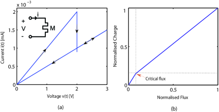
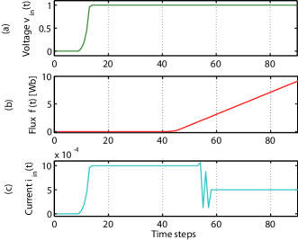
SPICE simulations with the macro-model of the memristor are shown in Figs. 9 and 10. In this particular simulation, a monotonically-increasing and piecewise-linear - function is assumed as the memristor characteristic. This function is shown in Fig. 9 (b). The simulated memristor has a value of when the flux is less than , but it becomes when the flux is equal or higher than . The critical flux () can be varied with the turn-on voltage of the switch in the macro-model. Fig. 9 (a) shows the pinched hysteresis characteristic of the memristor. The input voltage to the memristor is a ramp with a slope of . When the input voltage ramps up with a slope of , the memristance is and the slope of the current-voltage characteristics is before the the flux reaches to the . But when the flux becomes , the memristance value is changed to and the slope is now . After the input voltage reaches to the maximum point, it ramps down and the slope is maintained, because the memristance is still . Fig. 10 shows the memristor characteristics when a step input voltage is applied. Initially the memristance is , so the input current is . When the flux reaches to (), the memristance is and so the input current is now as predicted. The developed macro-model can be used to understand and predict the characteristics of a memristor.
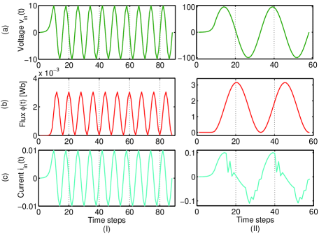
Now, if a sinusoidal voltage source is connected across the memristor model, the flux does not reach to so and . Fig. 11(I) shows the memristor characteristics when a sinusoidal input voltage is applied. As it is shown in Fig. 11(II), when the voltage source frequency reduces to , the flux linkage reaches to within . Based on this result, there are two levels of memristance, and then it changes to .
Another interesting study is needed to verify that the model is working properly when there is a parallel, series, RM (Resistor-Memristor), LM (Inductor-Memristor), or CM (Capacitor-Memristor) network. First of all, let us assume that there are two memristors with the same characteristic as shown in Fig. 9. Analysing series and parallel configurations of these memristors are demonstrated in Figs. 12(b) and 12(a), respectively. In both figures, the left - curve shows a single memristor.
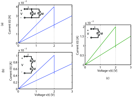
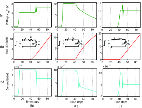
The simulation results show that the series and parallel configurations of memristors are the same as their resistor counterparts. It means the equivalent memristances, , of a two memristor in series and parallel are and , respectively, where is memristance of a single memristor. The second step is RM, LM, and CM networks. In these cases a step input voltage has been applied to circuits. As mentioned before for a single memristor based on the proposed model, while the flux linkage is less than or equal to the critical flux, , and when the flux is more than the critical flux value, , . Recall that the critical flux value based on the curve is . Figs. 13(R), 13(C), and 13(L) illustrate RM, CM, and LM circuits and their response to the input step voltage, respectively.
If we assume that the memristance value switches at time , then for , , and . Therefore, in the RM circuit we have, . For , and then , so . Likewise, when , , we have, and . Both cases have been verified by the simulation results.
In the LM circuit we have the same situation, so for , , , (), and . For , memristor current is . Memristor’s current changing is clearly shown in Fig. 13(L). The CM circuit simulation also verifies a change in time constant from to .
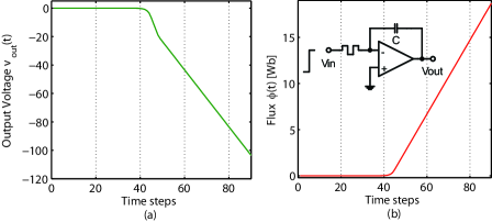
As another circuit example of using the new memristor model, an op-amp integrator has been chosen. The model of an op-amp and circuit configuration is shown in Fig. 14. If then we have and as the time constant of the circuit at and , respectively.
It is worth mentioning that, recently, a few simple SPICE macro-models have been proposed by Benderli and Wey (2009), Biolek et al. (2009b) and Zhang et al. (2009) but none of them consider the model response with different circuit elements types, which is an important step to verify the model correctness.
4 Interpreting memristor in Electromagnetic Theory
In his original paper Chua (1971) presented an argumentation based on electromagnetic field theory for the existence of the memristor. His motivation was to interpret the memristor in terms of the so-called quasi-static expansion of Maxwell’s equations. This expansion is usually used to give an explanation to the elements of circuit theory within the electromagnetic field theory.
Chua’s argumentation hints that a memristor might exist, it although never proved that this device can in fact be realised physically. In the following we describe how Chua argued for a memristor from a consideration of quasi-static expansion of Maxwell’s equations. To consider this expansion, we use Maxwell’s equations in their differential form,
| (20) | |||
| (21) | |||
| (22) | |||
| (23) |
where is electric field intensity (), is magnetic flux density (), is electric current density (), is electric charge density (), and are magnetic field intensity () and electric flux density (), and are divergence and curl operators.
The idea of a quasi-static expansion involves using a process of successive approximations for time-varying fields. The process allows us to study electric circuits in which time variations of electromagnetic field are slow, which is the case for electric circuits.
Consider an entire family of electromagnetic fields for which the time rate of change is variable. The family of fields can be described by a time-rate parameter which is time rate of change of charge density . We can express Maxwell’s equations in terms of the family time, , and the time derivative of can be written as
| (24) |
Other time derivatives can be expressed similarly. In terms of the family time, Maxwell’s equations take the form
| (25) |
which allow us to consider different values of the family time , corresponding to different time scales of excitation. Note that in Eqs. 25 , , , , and are also functions of and , along with the position .This allows us (Fano et al., 1960) to express, for example, as power series in :
| (26) |
where the zero and first orders are
| (27) | |||||
Along with these, a similar series of expressions for , , , and are obtained and can be inserted into Eqs. 25, with the assumption that every term in these series is differentiable with respect to and . This assumption permits us to write, for example,
| (28) |
and, when all terms are collected together on one side, this makes Eqs. 25 to take the form of a power series in that is equated to zero. For example, the first equation in Eq. 25 becomes
| (29) |
which must hold for all . This can be true if the coefficients of all powers of are separately equal to zero. The same applies to the second equation in Eqs. 25 and one then obtains the so-called th-order Maxwell’s equations, where For instance, the zero-order Maxwell’s equations are
| (30) | |||||
| (31) |
and the first-order Maxwell’s equations are
| (32) | |||||
| (33) |
The quasi-static fields are obtained from only the first two terms of the power series Eq. 29, while ignoring all the remaining terms and by taking . In this case we can approximate and .
Circuit theory, along with many other electromagnetic systems, can be explained by the zero-order and first-order Maxwell’s equations for which one obtains quasi-static fields as the solutions. The three classical circuit elements resistor, inductor, and capacitor can then be explained as electromagnetic systems whose quasi-static solutions correspond to certain combinations of the zero-order and the first-order solutions of Eqs. 30-33.
However, in this quasi-static explanation of circuit elements, an interesting possibility was unfortunately dismissed (Fano et al., 1960) as it was thought not to have any correspondence with an imaginable situation in circuit theory. This is the case when both the first-order electric and the first-order magnetic fields are not negligible. Chua argued that it is precisely this possibility that provides a hint towards the existence a fourth basic circuit device.
Chua’s argumentation goes as follows. Assume there exists a two-terminal device in which is related to , where these quantities are evaluated instantaneously. If this is the case then this device has the following two properties:
-
1.
Zero-order electric and magnetic fields are negligible when compared to the first-order fields i.e. and can be ignored.
-
2.
The device is made from non-linear material for which the first-order fields become related.
Assume that the relationships between the first-order fields are expressed as
| (34) | |||||
| (35) | |||||
| (36) |
where and are one-to-one continuous functions defined over space coordinates only. Combining Eq. 33, in which we have now , with Eq. 34 gives
| (37) |
As the curl operator does not involve time derivatives, and is defined over space coordinates, Eq. 37 says that the first-order fields and are related. This relation can be expressed by assuming a function and we can write
| (39) |
where operator is the composition of two (or more) functions. Also, as is a one-to-one continuous function, Eq. 35 can be re-expressed as
| (41) |
Eq. 41 predicts that an instantaneous relationship can be established between and that is realisable in a memristor. This completes Chua’s argumentation using Maxwell’s equations for a quasi-static representation of the electromagnetic field quantities of a memristor.
5 Conclusion
In this paper, we surveyed key aspects of the memristor as a promising nano-device. We also introduced a behavioural and SPICE macro-model for the memristor and reviewed Chua’s argumentation for the memristor by performing a quasi-static expansion of Maxwell’s equations. The SPICE macro-model has been simulated in PSpice and shows agreement with the actual memristor presented in Strukov et al. (2008). The model shows expected results in combination with a resistor, capacitor, or inductor. A new op-amp based memristor is also presented and tested.
Nanoelectronics not only deals with the nanometer scale, materials, and devices but implies a revolutionary change even in computing algorithms. The Von-Neumann architecture is the base architecture of all current computer systems. This architecture will need revision for carrying out computation with nano-devices and materials. There are many of different components, such as processors, memories, drivers, actuators and so on, but they are poor at mimicking the human brain. Therefore, for the next generation of computing, choosing a suitable architecture is the first step and requires deep understanding of relevant nano-device capabilities. Obviously, different capabilities might create many opportunities as well as challenges. At present, industry has pushed nanoelectronics research for highest possible compatibility with current devices and fabrication processes. However, the memristor motivates future work in nanoelectronics and nano-computing based on its capabilities.
In this paper we addressed some possible research gaps in the area of the memristor and demonstrated that further device and circuit modelling are urgently needed. The current approach to device modelling is to introduce a physical circuit model with a number of curve fitting parameters. However, such an approach has the limitation of requiring a large number of parameters. Using a non-linear drift model results in more accurate simulation at the cost of a much more complicated set of mathematical equations. Initially behavioural modelling can be utilised, nonetheless a greater modelling effort is needed to accommodate both the defect and process variation issues. An interesting follow up would be the development of mapping models based on the memristor to neuronmorphic systems that deal with architectural level challenges, such as defect-tolerance and integration into current integrated circuit technologies.
6 Acknowledgements
We would like to thank Leon Chua, at UC Berkeley, for useful discussion and correspondence. This work was partially supported by grant No. R33-2008-000-1040-0 from the World Class University (WCU) project of MEST and KOSEF through CBNU is gratefully acknowledged.
References
- Beck et al. [2000] A. Beck, J. G. Bednorz, C. Gerber, C. Rossel, and D. Widmer. Reproducible switching effect in thin oxide films for memory applications. Applied Physics Letters, 77(1), 2000.
- Benderli and Wey [2009] S. Benderli and T. A. Wey. On SPICE macromodelling of TiO2 memristors. Electronics Letters, 45(7):377–379, 2009.
- Biolek et al. [2009a] D. Biolek, Z. Biolek, and V. Biolková. SPICE modeling of memristive, memcapacitative and meminductive systems. In European Conference on Circuit Theory and Design, ECCTD, pages 249–252, Aug. 2009a.
- Biolek et al. [2009b] Z. Biolek, D. Biolek, and V. Biolková. SPICE model of memristor with nonlinear dopant drift. Radioengineering J., 18(2):211, 2009b.
- Blanc and Staebler [1971] J. Blanc and D. L. Staebler. Electrocoloration in SrTiO3: Vacancy drift and oxidation-reduction of transition metals. Phys. Rev. B, 4(10):3548–3557, 1971.
- Buot and Rajagopal [1994] F. A. Buot and A. K. Rajagopal. Binary information storage at zero bias in quantum-well diodes. Journal of Applied Physics, 76(9):5552–5560, 1994.
- Chen et al. [2009] M. Z. Q. Chen, C. Papageorgiou, F. Scheibe, F. C. Wang, and M. C. Smith. The missing mechanical circuit element. IEEE Circuits and Systems Magazine, 9(1):10–26, 2009.
- Chen and Wang [2009] Y. Chen and X. Wang. Compact modeling and corner analysis of spintronic memristor. In IEEE/ACM International Symposium on Nanoscale Architectures, NANOARCH, pages 7–12, July 2009.
- Chua [1968] L. O. Chua. Synthesis of new nonlinear network elements. Proceedings of the IEEE, 56(8):1325–1340, 1968.
- Chua [1971] L. O. Chua. Memristor - the missing circuit element. IEEE Transactions on Circuit Theory, 18(5):507–519, 1971.
- Chua and Kang [1976] L. O. Chua and S. M. Kang. Memristive devices and systems. Proceedings of the IEEE, 64(2):209–223, 1976.
- Delgado [2009] A. Delgado. Input-output linearization of memristive systems. In IEEE Nanotechnology Materials and Devices Conference, NMDC, pages 154–157, June 2009.
- Di Ventra et al. [2009] M. Di Ventra, Y. V. Pershin, and L. O. Chua. Circuit elements with memory: Memristors, memcapacitors, and meminductors. Proceedings of the IEEE, 97(10):1717–1724, Oct. 2009.
- Driscoll et al. [2009] T. Driscoll, H. T. Kim, B. G. Chae, M. Di Ventra, and D. N. Basov. Phase-transition driven memristive system. Applied Physics Letters, 95(4):art. no. 043503, 2009.
- Fano et al. [1960] R. M. Fano, L. J. Chu, R. B. Adler, and J. A. Dreesen. Electromagnetic Fields, Energy, and Forces. John Wiley and Sons, New York, 1960.
- Formula1 [2007] Formula1. FIA letter puts McLaren drivers in spy scandal spotlight, Sep. 2007. URL http://www.formula1.com/news/headlines/2007/9/6723.html.
- Gergel-Hackett et al. [2009] N. Gergel-Hackett, B. Hamadani, B. Dunlap, J. Suehle, C. Richter, C. Hacker, and D. Gundlach. A flexible solution-processed memristor. IEEE Electron Device Letters, 30(7):706–708, 2009.
- Ignatiev et al. [2008] A. Ignatiev, N. J. Wu, X. Chen, Y. B. Nian, C. Papagianni, S. Q. Liu, and J. Strozier. Resistance switching in oxide thin films. Phase Transitions, 7(8):791–806, 2008.
- Itoh and Chua [2008] M. Itoh and L. O. Chua. Memristor oscillators. International Journal of Bifurcation and Chaos, IJBC, 18(11):3183–3206, 2008.
- ITRS [2007] ITRS. International Technology Roadmap for Semiconductors, 2007. URL Available online at http://public.itrs.net.
- Joglekar and Wolf [2009] Y. N. Joglekar and S. J. Wolf. The elusive memristor: properties of basic electrical circuits. European Journal of Physics, 30(4):661, 2009.
- Jones [2009] R. Jones. Computing with molecules. Nature Nanotechnology, 4(4):207, 2009.
- Kang [1975] S. M. Kang. On The Modeling of Some Classes of Nonlinear Devices and Systems. Doctoral dissertation in Electrical and Electronics Engineering, 76-15-251, University of California, Berkeley, CA, 1975.
- Kavehei et al. [2009] O. Kavehei, Y. S. Kim, A. Iqbal, K. Eshraghian, S. F. Al-Sarawi, and D. Abbott. The fourth element: Insights into the memristor. In the IEEE International Conference on Communications, Circuits and Systems, ICCCAS, pages 921–927, July 2009.
- Kim et al. [2009a] K. H. Kim, B. S. Kang, M. J. Lee, S. E. Ahn, C. B. Lee, G. Stefanovich, W. X. Xianyu, C. J. Kim, and Y. Park. Multilevel programmable oxide diode for cross-point memory by electrical-pulse-induced resistance change. IEEE Electron Device Letters, 30(10):1036–1038, 2009a.
- Kim et al. [2009b] T. H. Kim, E. Y. Jang, N. J. Lee, D. J. Choi, K. Lee, J. T. Jang, J. S. Choi, S. H. Moon, and J. Cheon. Nanoparticle assemblies as memristors. Nano Letters, 9(6):2229–2233, 2009b.
- Krieger et al. [2001] J. H. Krieger, S. V. Trubin, S. B. Vaschenko, and N. F. Yudanov. Molecular analogue memory cell based on electrical switching and memory in molecular thin films. Synthetic Metals, 122(1):199–202, 2001.
- Lehtonen and Laiho [2009] E. Lehtonen and M. Laiho. Stateful implication logic with memristors. In IEEE/ACM International Symposium on Nanoscale Architectures, NANOARCH, pages 33–36, July 2009.
- Lewis and Lee [2009] D. L. Lewis and H. H. S. Lee. Architectural evaluation of 3D stacked RRAM caches. In IEEE International 3D System Integration Conference, 3D-IC, page To appear, San Francisco, CA, Sept. 28-30 2009.
- Li et al. [2009] C. Li, M. Wei, and J. Yu. Chaos generator based on a PWL memristor. In the IEEE International Conference on Communications, Circuits and Systems, ICCCAS, pages 944–947, July 2009.
- Lin and Wang [2009] Z. H. Lin and H. X. Wang. Image encryption based on chaos with PWL memristor in Chua’s circuit. In the IEEE International Conference on Communications, Circuits and Systems, ICCCAS, pages 964–968, July 2009.
- Liu et al. [2006] S. Liu, N. Wu, A. Ignatiev, and J. Li. Electric-pulse-induced capacitance change effect in perovskite oxide thin films. Journal of Applied Physics, 100(5):1–3, 2006.
- Mallégol [2003] S. Mallégol. Caractérisation et Application de Matériaux Composites Nanostructurés á la Réalisation de Dispositifs Hyperfréquences Non Réciproques. Doctoral dissertation in Electronic, (in French), Université de Bretagne Occidentale, France, 2003.
- Oster [1974] G. Oster. A note on memristors. IEEE Transactions on Circuits and Systems, 21(1):152–152, 1974.
- Oster [1973] G. F. Oster. The Memristor: A New Bond Graph Element. Journal of Dynamic Systems, Measurement, and Control, pages 1–4, 1973.
- Raja and Mourad [2009] T. Raja and S. Mourad. Digital logic implementation in memristor-based crossbars. In the IEEE International Conference on Communications, Circuits and Systems, ICCCAS, pages 939–943, July 2009.
- Shin et al. [2009] S. Shin, K. Kim, and S. M. Kang. Memristor-based fine resolution programmable resistance and its applications. In the IEEE International Conference on Communications, Circuits and Systems, ICCCAS, pages 948–951, July 2009.
- Simmons [1963] J. G. Simmons. Generalized formula for the electric tunnel effect between similar electrodes separated by a thin insulating film. Journal of Applied Physics, 34(6):1793–1803, 1963.
- Simmons and Verderber [1967] J. G. Simmons and R. R. Verderber. New conduction and reversible memory phenomena in thin insulating films. Proceedings of the Royal Society of London. Series A, Mathematical and Physical Sciences, 301(1464):77–102, 1967.
- Smith [2002] M. C. Smith. Synthesis of mechanical networks: The inerter. IEEE Transactions on Automatic Control, 47(10):1648–1662, 2002.
- Strukov and Williams [2009] D. B. Strukov and R. S. Williams. Exponential ionic drift: fast switching and low volatility of thin-film memristors. Applied Physics A: Materials Science & Processing, 94(3):515–519, 2009.
- Strukov et al. [2008] D. B. Strukov, G. S. Snider, D. R. Stewart, and R. S. Williams. The missing memristor found. Nature, 453(7191):80–83, 2008.
- Sun et al. [2009a] W. Sun, C. Li, and J. Yu. A simple memristor based chaotic oscillator. In the IEEE International Conference on Communications, Circuits and Systems, ICCCAS, pages 952–954, July 2009a.
- Sun et al. [2009b] W. Sun, C. Li, and J. Yu. A memristor based chaotic oscillator. In the IEEE International Conference on Communications, Circuits and Systems, ICCCAS, pages 955–957, July 2009b.
- Swaroop et al. [1998] B. Swaroop, W. C. West, G. Martinez, M. N. Kozicki, and L. A. Akers. Programmable current mode hebbian learning neural network using programmable metallization cell. In the IEEE International Symposium on Circuits and Systems, ISCAS’98, volume 3, pages 33–36, May 1998.
- Tavakoli and Sarpeshkar [2005] M. Tavakoli and R. Sarpeshkar. A sinh resistor and its application to tanh linearization. IEEE Journal of Solid-State Circuits, 40(2):536–543, 2005.
- Thakoor et al. [1990] S. Thakoor, A. Moopenn, T. Daud, and A. P. Thakoor. Solid-state thin-film memistor for electronic neural networks. Journal of Applied Physics, 67(6):3132–3135, 1990.
- Tulina et al. [2008] N. A. Tulina, I. Y. Borisenko, and V. V. Sirotkin. Reproducible resistive switching effect for memory applications in heterocontacts based on strongly correlated electron systems. Physics Letters A, 372(44):6681–6686, 2008.
- Varghese and Gandhi [2009] D. Varghese and G. Gandhi. Memristor based high linear range differential pair. In the IEEE International Conference on Communications, Circuits and Systems, ICCCAS, pages 935–938, July 2009.
- Wang et al. [2009a] D. Wang, Z. Hu, X. Yu, and J. Yu. A PWL model of memristor and its application example. In the IEEE International Conference on Communications, Circuits and Systems, ICCCAS, pages 932–934, July 2009a.
- Wang et al. [2009b] D. Wang, H. Zhao, and J. Yu. Chaos in memristor based Murali-Lakshmanan-Chua circuit. In the IEEE International Conference on Communications, Circuits and Systems, ICCCAS, pages 958–960, July 2009b.
- Wang [2008] F. Y. Wang. Memristor for introductory physics. Preprint arXiv:0808.0286, 2008.
- Wang et al. [2009c] W. Wang, Q. Yu, C. Xu, and Y. Cui. Study of filter characteristics based on PWL memristor. In the IEEE International Conference on Communications, Circuits and Systems, ICCCAS, pages 969–973, July 2009c.
- Wang et al. [2009d] X. Wang, Y. Chen, H. Xi, H. Li, and D. Dimitrov. Spintronic memristor through spin-torque-induced magnetization motion. IEEE Electron Device Letters, 30(3):294–297, 2009d.
- Waser and Masakazu [2007] R. Waser and A. Masakazu. Nanoionics-based resistive switching memories. Nature Materials, 6(11):833–840, 2007.
- Waser et al. [2009] R. Waser, R. Dittmann, G. Staikov, and K. Szot. Redox-based resistive switching memories - nanoionic mechanisms, prospects, and challenges. Advanced Materials, 21(25-26):2632–2663, 2009.
- Widrow et al. [1960] B. Widrow, A. Force, and A. S. Corps. Adaptive “adaline” neuron using chemical “memistors”. Technical Report Technical Report: 1553-2, Stanford Electronics Laboratories, 1960.
- Williams [2008] R. Williams. How we found the missing memristor. IEEE Spectrum, 45(12):28–35, 2008.
- Witrisal [2009] K. Witrisal. Memristor-based stored-reference receiver - the UWB solution? Electronics Letters, 45(14):713–714, 2009.
- Yang et al. [2008] J. J. Yang, M. D. Pickett, X. Li, D. A. A. Ohlberg, D. R. Stewart, and R. S. Williams. Memristive switching mechanism for metal/oxide/metal nanodevices. Nature Nanotechnology, 3(7):429–433, 2008.
- Yu et al. [2009] Q. Yu, Z. Qin, J. Yu, and Y. Mao. Transmission characteristics study of memristors based op-amp circuits. In the IEEE International Conference on Communications, Circuits and Systems, ICCCAS, pages 974–977, July 2009.
- Zhang et al. [2009] Y. Zhang, X. Zhang, and J. Yu. Approximated SPICE model for memristor. In the IEEE International Conference on Communications, Circuits and Systems, ICCCAS, pages 928–931, July 2009.