Graphane Nanoribbons: A Theoretical Study
Abstract
In this study, we investigate the electronic and magnetic properties of graphane nanoribbons. We find that zigzag and armchair graphane nanoribbons with H-passivated edges are nonmagnetic semiconductors. While bare armchair nanoribbons are also nonmagnetic, adjacent dangling bonds of bare zigzag nanoribbons have antiferromagnetic ordering at the same edge. Band gaps of the H-passivated zigzag and armchair nanoribbons exponentially depend on their width. Detailed analysis of adsorption of C, O, Si, Ti, V, Fe, Ge and Pt atoms on the graphane ribbon surface reveal that functionalization of graphane nanoribbons is possible via these adatoms. It is found that C, O, V and Pt atoms have tendency to replace H atoms of graphane. We showed that significant spin polarizations in graphane can be achieved through creation of domains of H-vacancies and CH-divacancies.
pacs:
73.22.Pr, 75.75.-c, 61.48.-c, 62.23.KnI Introduction
After the synthesis of two dimensional (2D) graphenenovo1 ; novo2 ; zhang ; berger ; kats ; geim , its nanoribbons (NRs) have been a subject of interest, both experimentallyhan ; li and theoretically.lee ; barone ; abanin ; cresti ; ezawa0 ; gunlycke2 ; hod1 Advances in experimental techniques are paving the way for integrating the exceptional electrical, optical and magnetic functionalities of these nanometer-sized materials into future electronic technology. In addition to numerous theoretical and experimental works on graphene and its NRs, research efforts have been also devoted to synthesize its various derivatives. Notably, the synthesis of a 2D hydrocarbon in honeycomb structure,elias namely graphane, followed its prediction through theoretical works.sofo ; boukhvalov Detailed analysis of hydrogenation processes of graphene leading to graphane and the existence of hydrogen (H) frustrations were discussed very recently.Graphene to graphane Furthermore, it was reported that graphane NRs have more favorable formation energies than experimentally available graphene ribbons. yafei Recently, we reported the possibility of obtaining magnetization through dehydrogenation of domains on 2D graphane.hasan-can Modification of electronic structure of graphane by introducing either a hydroxyl group or a H-vacancy was also investigated with GW self-energy calculations. lebeque Although there are several recent studies on graphane, electrical and magnetic properties of its NRs have remained unexplored.
Recent advances in graphane have motivated us to explore the properties of zigzag and armchair graphane NRs. In this paper, using first-principles plane wave method within the density functional theory (DFT) we investigated the electronic and magnetic properties of bare and H- passivated graphane NRs. We also explored the effects of specific imperfections on these properties. These are various foreign atoms adsorbed on the surfaces of graphane NRs, vacancies and edge roughness. We found that these imperfections can attribute interesting functionalities by modifying the electronic and magnetic properties of graphane NRs.
II Methods
We perform first-principles calculationskresse within DFT using projector augmented wave (PAW) potentialspaw and approximate exchange-correlation functional by spin polarized local density approximationlda (LDA). Kinetic energy cutoff for plane-wave basis set is taken as 500 eV. In the self-consistent potential and total energy calculations of 2D graphane a set of (35x35x1) k-point sampling is used for Brillouin zone (BZ) integration. The convergence criterion of self consistent calculations for ionic relaxations is eV between two consecutive steps. By using the conjugate gradient method, all atomic positions and unit cells are optimized until the atomic forces are less than 0.03 eV/Å. Pressures on the lattice unit cell are decreased to values less than 1.0 kBar.
In order to correct the energy bands and band gap values obtained by LDA, frequency-dependent GW0 calculations are carried out.gw Screened Coulomb potential W, is kept fixed at initial DFT value W0 and Green’s function G, is iterated five times. GW0 self-energy calculations are carried out with Å vacuum spacing, default cut-off potential, 160 bands and 64 grid points.
Graphane NRs are treated by the supercell geometry within periodic boundary conditions. Vacuum spacing of at least Å is placed between adjacent graphane NRs to hinder the interactions. In specific cases double unit cell is used in our calculations to allow the possible antiferromagnetic (AFM) orderings along the ribbon edges. Reciprocal space integrations are carried out with 1x1x15 Monkhorst-Pack k-point grids.
III Two Dimensional Graphane
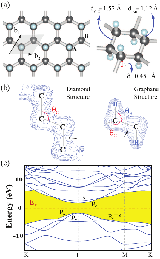
For a better understanding of graphane NRs we start with 2D graphane which is derived from the hydrogenation of graphene, where each carbon atom is saturated by a single hydrogen atom. Accordingly, the primitive cell of graphane consists of two carbon and two hydrogen atoms. Chair like configuration of infinite sheet of 2D graphane is formed, whereby each carbon atoms of A- and B-type sublattices are saturated by hydrogen atoms from above and below, respectively, as described in Fig. 1(a). This is known as the most favorable and stable hydrocarbon conformation.sofo ; hasan-can The planar graphene honeycomb structure, which is stabilized by planar -hybrid orbitals and -bonding between adjacent perpendicular -orbitals is puckered (buckled) as a result of the adsorption of H atoms, whereby a single C atom is bound to three adjacent C atoms and a single H atom through ’tetrahedrally coordinated’ -like hybrid orbitals. The buckling, , i.e. the perpendicular distance between A-type and B-type carbon sublattices, is calculated to be 0.45 Å. As a result, the lattice constant of graphene increases from 2.46 Å to 2.51 Å and hence the C-C and C-H bond lengths become 1.52 and 1.12 Å, respectively, as indicated in Fig. 1(a). The charge density contour plots given in Fig. 1(b) indicate that the charge distribution in graphane especially around the C-C bond is reminiscent of that in tetrahedrally coordinated diamond. In graphane, the angle between H-C and C-C bonds and between adjacent C-C bonds are and , respectively. The mean value of these angles is equal to the tetrahedral angle of diamond. The maximum of the C-C bond charge in diamond and in graphane are found to be and e/Å3, respectively.
| Material | |||||||||||||||
|---|---|---|---|---|---|---|---|---|---|---|---|---|---|---|---|
| (1x1) unit cell | (Å) | (Å) | (Å) | (Å) | (deg) | (deg) | () | () | () | () | ( ) | () | () | () | |
| Graphene | 2.46 | 1.42 | - | - | 120 | - | 0.00 | 0.00 | 20.16 | 17.87 | - | - | 4.77 | 335lee-science | 0.16 |
| Graphane | 2.51 | 1.52 | 1.12 | 0.45 | 111.51 | 107.35 | 3.42 | 5.97 | 27.65 | 23.57 | 3.74 | 2.84 | 4.97 | 243topsakal-graphane | 0.07 |
The cohesive energy of graphane (per unit cell) relative to free C and H atoms is obtained from , where and are the total energies of single free C, and free H, whereas is the total energy of graphane. The cohesive energy depends whether the energies of magnetic or nonmagnetic (NM) states of free C and free H atoms are considered. Here the cohesive energy per unit cell of graphane is calculated to be 23.57 (27.65) eV by considering the magnetic (nonmagnetic) states of free atoms. As for the average C-H bond energy, one can use the formula where is the total energy of graphene. The calculated value is 2.84 (3.74 for nonmagnetic case). We reportedhasan-can that the desorption of a single H atom from the graphane is an endothermic reaction with an energy of 4.79 eV. When compared with the energy of C-H bond, the desorption energy of single H is larger, since the single H removal creates reconstruction of nearby atoms which further reduces the total energy of the system.
Due to -saturation of C atoms, 2D graphane is a NM semiconductor with a direct band gap of 3.42 eV as shown in Fig. 1(c). However, this band gap, which is underestimated within DFT, is corrected by GW0 approximation to become 5.97 eV.hasan-can ; lebeque While the top of the valence band originates from - and -orbitals of C atoms, the bottom of the conduction band has C- orbital character. Earlier, we also calculatehasan-can the phonon modes of infinite 2D graphane, which yield all real frequencies in BZ. Having all frequencies positive indicate the stability of graphane structure.
An exceptional feature of graphane is related with its interesting charging configuration. While graphene has a covalent bonding, upon the saturation of each C atom by a single H atom, a charge of 0.1 electrons is transferred from H to C. At the end, the negatively charged bilayer of carbon atoms becomes sandwiched between positively charged H layers. Graphane having this charging has the photoelectric threshold (work function) calculated to be =4.97 eV, which is 0.2 eV larger than that of graphene. In Table 1, we presented the calculated values related with structure, energy bands, photoelectric threshold etc. of graphane and graphene for the sake of comparison. To be complete Table 1 also includes calculated elastic constants such as in-plane stiffnessbrandbyge , where is the total energy of the system under strain, is the uniaxial strain and is the area of the unit cell] and Poisson’s ratiohasan-ansiklopedi .
IV Graphane Nanoribbons
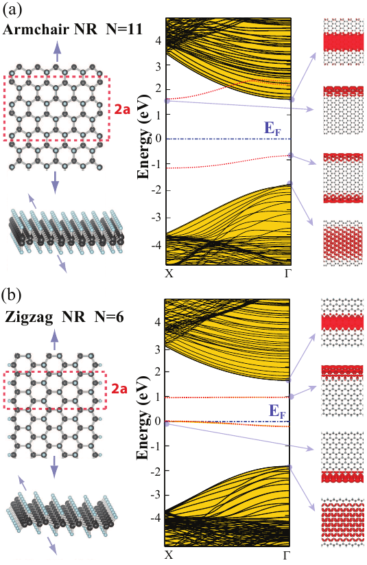
The nanoribbons cut from a 2D graphane are structures providing important features for various technological applications. Two major families of graphane NRs are distinguished depending on their orientations; namely armchair, and zigzag graphane NRs. Apart from the orientation, graphane NRs are characterized by their widths. For armchair graphane NRs, the width, , is defined by the number of C-C dimers in the unit cell which are parallel to the axis of the nanoribbon; for zigzag graphane NRs, denotes the number of zigzag carbon chains along the nanoribbon axis. The electronic structure changes depending on whether the dangling bonds of carbon atoms at the edge are free (bare) or passivated by single H atoms. In Fig. 2(a) and 2(b) we show the atomic and electronic structure of armchair and zigzag graphane NRs with =11 and =6, respectively.
Bare armchair graphane NR is a NM indirect band gap semiconductor, since the electrons at the dangling orbitals are paired. The band gap of 2D graphane is reduced due to the bands of edge states of dangling bonds occurring in the band gap. The charge density analysis of these edge state bands presented in Fig. 2(a) clearly shows that they are localized at the edges of the NR. Upon hydrogen passivation of the threefold coordinated edge atoms, the edge state bands in the gap disappear and the direct band gap opens up.
Similar to armchair graphane NRs, the dangling bonds of the threefold coordinated carbon atoms at both edges of zigzag graphane NRs give rise to edge states in the band gap. Owing to relatively large distance between adjacent dangling bonds and hence their relatively smaller coupling, they have a minute dispersion. Charge density isosurfaces of these edge states confirm their localization at the edges. Also, owing to their weak coupling the spins of adjacent dangling bonds cannot be paired. Consequently, each carbon atom at the zigzag edge attains a magnetic moment of 1 Bohr magneton (). The ordering of these magnetic moments is however dramatically different from that of the zigzag graphene NRs. The significant coupling between two spin states at different edges gives rise to AFM ordering along the graphene edge.
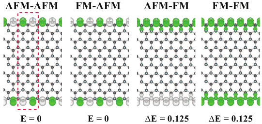
The physical origin of the magnetic interactions between the edges of graphitic fragments was treated earlier.edge-states For zigzag graphene nanoribbon, collective alignment of the magnetic moments along the same ribbon edge through the ferromagnetic (FM) interaction, but AFM ordering between opposite edges is attributed to magnetic tail interactions. The magnetic ordering of a wide zigzag graphane NRs ( 2 nm) are examined in a supercell comprising two unit cells, whereby antiferromagnetic ordering between adjacent dangling bonds at the same edge is allowed. We consider four different orderings, such as AFM-AFM (where, respectively, the ordering of magnetic moments at the atoms located at different and same edge are antiferromagnetic), FM-AFM, AFM-FM and FM-FM as described in Fig. 3. Here the difference charge density is defined as the where is spin up (down) charge. Since the magnetic interaction between two edges vanishes, AFM-AFM and FM-AFM orderings have the same total energy corresponding to the ground state. These orderings are 125 meV energetically more favorable than the AFM-FM and FM-FM orderings. From this analysis it is revealed that AFM spin alignment between adjacent atoms at the same edge is preferred by the zigzag graphane NRs. FM ordering between two spins has 62.5 meV higher energy. For zigzag graphane NR with =6, the magnetic coupling between two edges is negligible and hence either AFM-AFM or FM-AFM orderings have the same energy and they are ground states. However, when the width of the nanoribbon is less than 12 Å the degeneracy of AFM-AFM and FM-AFM states is broken. The bare zigzag graphane NR is an indirect and antiferromagnetic semiconductor with an indirect band gap relatively smaller than that of 2D graphane. However, it becomes NM, direct band gap semiconductor upon passivation of the dangling bonds. Also the magnetic edge states disappear and band gap becomes larger.
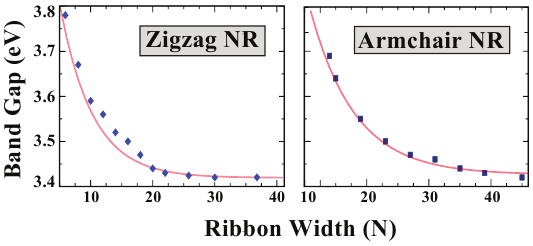
The value of the band gap of graphane NRs can differ from that of parent 2D structure due to a combined effects of quantum confinement, edge state bands as well as folding in the direction perpendicular to the NR axis. We note that the band gap of graphane NR depends on its width given by N. However, the quantum confinement effect is not as emphasized as that found in graphene NR. In Fig. 4, H-passivated armchair and zigzag graphane NRs display a quantum confinement effect, namely the band gap reduction with increasing width or . This behavior is fitted to an expression as:
| (1) |
Here and are fitting parameters. The values of and are found to be 1.18 eV and 0.19 for zigzag graphane NRs (2.15 eV and 0.14 for armchair graphane NRs). The band gaps of both types of graphane NRs go to 3.42 eV as . Considering the GW0 corrected value of the band gap, 5.97 eV, the above fitting can be expressed as assuming that the same scissor operation is applicable for graphane NRs. Apparently, the band gap values of graphane NRs calculated using DFT are underestimated and hence their values are expected to occur 2.5 eV larger than presented in Fig. 4. Unfortunately, GW0 self-energy corrections cannot be performed for graphane NRs due to large computational time. We note that the variation of band gap is relevant for for zigzag graphane NRs and for armchair graphane NRs. In Ref.[yafei, ] the band gaps of hydrogen saturated graphane NRs were calculated for using Generalized Gradient Approximation (GGA). In the present study band gaps are calculated for using LDA. The hydrogenated graphane NRs included in both studies, namely those , are in good agreement. Largest band gap difference of 0.1 eV found between two studies is attributed to different approximations (i.e LDA versus GGA) in representing exchange-correlation potential.
V Functionalization of Graphane NRs by Adatoms
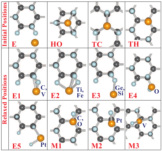
Adsorption of adatoms is widely used and an efficient way to provide new functionalities to structures in nanoscale applications.hasan-prb ; can1 ; cohen-adsorp Adsorption of C, O, Si, Ge, Pt, V, Fe and Ti adatoms on graphane nanoribbons is investigated by using (1x1x6) supercell of H-passivated armchair graphane NR having =8. Adsorption geometry is determined by calculating the lowest binding energy corresponding to the optimized structures. To this end, the binding energies of adatoms at four initial sites described in Fig. 5: These are edge site E; hollow site HO, top site of the carbon TC and top site of the hydrogen atom TH in the middle of NR. The stable binding sites are determined upon structure relaxation. In the same figure the positions of adatoms after relaxation are also shown. Binding energies () of these atoms are calculated by using the expression
| (2) |
in terms of the total energies of the optimized structure of graphane NR with adatom, ; bare NR, and free adatom, . Owing to the large graphane nanoribbon unit cell, k-point sampling is done only along the axis of the ribbon. All the energies are calculated in the same unit cell and obtained from the lowest ground-state total energies (either magnetic or nonmagnetic). Initially, at least 2 Å distance between adatom and outermost graphane atom is provided to find the relaxation site of adatom on the ribbon.
An atom adsorbed on graphane NR may give rise to resonance states in the valence and conduction bands, and also localized states in the band gap. Owing to the periodic boundary conditions, the energy levels associated with these adatoms may form energy bands. Since we consider a supercell consisting of six unit cell of H-passivated armchair graphane NR, the adatom-adatom distance is large and prevents coupling between adjacent adatoms. In this respect, the flat bands associated with adatoms can mimic either resonance or localized states relevant for dilute doping.
In Table 2, we present nearest neighbor distances between adatom and H () and C (), binding energy (), total magnetic moment of the system (), charge transfer between adatom and adsorbate (). Since the inversion symmetry of graphane can be broken by the adsorption of an atom, a net electric-dipole moment can be induced thereof. Thus electric dipole moment values calculated in the direction normal to graphane NR surface p, induced by adatom are also listed in Table 2. Photoelectric threshold of the adatom+graphane system perpendicular to the plane of NR, , is calculated by the difference of the electrostatic potential at distances where the gradient of it is negligible and the Fermi level of the adsorbed system. It should be noted that both p and is relevant only for uniform coverage of graphane. For a dilute impurity, these calculated values converge to that of armchair graphane. When the width of armchair graphane NR is large enough, one expects the photoelectric threshold, , and dipole moment, p, to converge to 4.97 eV and 0 eÅ, respectively.hasan-can
| p | ||||||||||
|---|---|---|---|---|---|---|---|---|---|---|
| (Å) | (Å) | () | (e) | (eÅ) | : Spin-up, : Spin-down States | |||||
| C | 1.27 | 2.05 | 1.10 | 2.00 | -0.28 | 3.85 | 0.02 | 0.45, 0.88, 2.17, 2.88, 3.53, 3.64 | ||
| 1.12 | 1.45 | 3.99 | 0.00 | -0.18 | 4.02 | 0.34 | 0.72, 1.52 | |||
| O | 0.98 | 1.42 | 5.67 | 0.00 | -1.23 | 4.63 | 0.19 | -0.87, -0.50, -0.22, 0.00, 4.80 | ||
| 0.98 | 1.43 | 5.89 | 0.00 | -1.27 | 4.59 | 0.11 | -1.16, -1.02, -0.66, 4.08 | |||
| Si | 1.88 | 2.65 | 0.54 | 2.00 | 0.03 | 3.42 | 0.03 | 1.20, 1.34, 2.36, 2.43, 2.56, 2.95 | ||
| 1.84 | 3.00 | 0.68 | 2.00 | -0.02 | 3.59 | 0.42 | 1.23, 1.24, 1.93, 2.42, 2.45, 2.46 | |||
| Ti | 1.97 | 2.16 | 0.81 | 2.00 | 0.19 | 2.65 | 0.27 | 1.77, 2.30, 2.34, 2.43, 2.81, 2.89, 3.11 | ||
| 1.95 | 2.52 | 0.89 | 3.91 | 0.31 | 2.16 | 0.92 | 2.18, 2.48, 2.49, 2.95, 3.18, 3.27, 3.28 | |||
| V | 1.99 | 2.40 | 0.54 | 5.00 | 0.14 | 2.56 | 0.22 | 1.49, 2.10, 2.38, 2.43, 2.50, 2.70, 3.16 | ||
| 1.71 | 2.07 | 1.24 | 3.00 | 0.93 | 3.13 | 0.43 | 0.10, 0.49, 1.45, 1.60, 1.84, 2.20, 3.03 | |||
| Fe | 1.90 | 2.15 | 0.57 | 4.00 | 0.05 | 3.21 | 0.36 | -0.42, -0.27, -0.08, -0.03, 0.03, 1.48, 1.59 | ||
| 1.95 | 2.83 | 0.65 | 4.00 | 0.07 | 2.98 | 0.53 | -1.15, -0.75, -0.57, -0.41, -0.34, 0.09 , 1.39 | |||
| Ge | 1.96 | 2.71 | 0.48 | 2.00 | 0.00 | 3.38 | 0.03 | 1.27, 1.38, 2.25, 2.41, 2.52, 2.81 | ||
| 1.91 | 3.06 | 0.62 | 2.00 | -0.02 | 3.55 | 0.36 | 1.30, 1.31, 1.89, 2.38, 2.42, 2.43 | |||
| Pt | 1.56 | 2.00 | 3.79 | 0.00 | -0.13 | 4.57 | -0.09 | -0.78, -0.36, -0.13, 0.13, 2.76 | ||
| 1.54 | 2.04 | 3.50 | 0.00 | -0.18 | 4.30 | 0.34 | -0.36, -0.21, 0.38, 2.58, 3.43 |
We found that some atoms, such as C, O, V and Pt that are adsorbed on the H-passivated armchair graphane NR surface show a tendency to remove H atoms from graphane surface. Since the single atoms of C, O, V and Pt have rather high binding energy, it seems possible to create graphene domains on graphane by striping H atoms but covering the domain by adsorbed atoms. Independent of their initial position, C and O atoms are adsorbed to carbon atoms of graphane by replacing H atoms. A typical binding configuration of C and O is indicated as M1 in Fig. 5. Adsorption of C and O atoms occur at the middle of nanoribbon with strong binding energies of 5.89 and 3.99 eV, respectively. The resulting system is NM. Binding structures of Pt and V, which also remove H atom from the host C atom of graphane, are also shown in the same figure.
Although H has very low binding energy (and hence is not shown in Table 2), it may be important for striping H atoms from graphane. Upon all geometry relaxations from different initial conditions, single adsorbed H atom prefers to bind on top of H atom of graphane and forms H2 molecule which is weakly bound to the nearest C atom. The binding energy of H2 molecule is calculated to be meV.
VI Vacancies in Graphane NRs
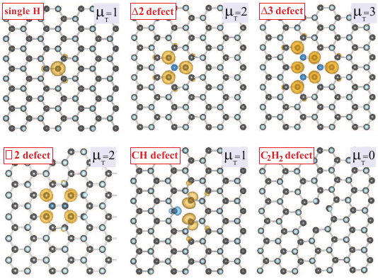
In our recent studyhasan-can , we showed that a graphane, which has a NM ground state, can be made magnetic simply by removing hydrogen atoms from the uniform hydrogen layers adsorbed on its both sides. It was found that the magnetization depends on whether the defect region is one-sided or two-sided. It was also shown that in certain circumstances remarkably large magnetic moments can be attained in a small domain on the sheet of graphane. Experimentally, removal of surface hydrogen atoms by using laser beam resonating with surface-atom bondlaser , ionic vapor applicationbreaux and subnanometer Pt clustersvajda are reported before. Since it is revealed that the double-sided vacancies give higher magnetic moments we focus on these type of vacancies on the nanoribbons.
In this section we consider six different types of vacancies in a bare armchair graphane NR with =15. Upon desorption of a single hydrogen atom, as shown in Fig. 6, local bonding through -hybrid orbital is retransformed into planar - and perpendicular -orbitals. At the vacancy site one electron accommodated by the dangling -orbital becomes unpaired and hence contributes to the magnetization by 1 . We also calculated that a single H-vacancy located at the center of the NR has 70 meV lower energy than that located near the edge of the ribbon.
The situation is rather intriguing for the magnetization of large domains of hydrogen vacancies. As in the case of single H-vacancy, leading to transformation of -bonding into planar -bonding, triangular , and rectangular shaped large graphene islands can be created by removing H atoms hence by creating H-vacancy domains. As shown in Fig. 6, hydrogen desorbed triangle-shaped island consisting of carbon atom at its each edge is defined as n-type H-vacancy. Therefore, a n-type vacancy domain can be obtained by removing H atom from top side and H atom from down side of the graphane nanoribbon. This means that -orbital electrons freed from A-type and -orbital electrons freed from B-type sublattice C atoms. According to the Lieb’s theorem Lieb net magnetic moment of such a system can be calculated from the difference between the sublattice atoms. For triangle vacancies this difference is simply equal to and thus the n-vacancy domain has net magnetic moment with . However, the -type domains does not yield large magnetic moments and have values between 0 and 2 . It is seen that magnetic interactions in double-sided triangular and square H-vacancy domains resulting in net magnetic moments are relatively straightforward and are in good agreement with Lieb’s theorem.
We also consider CH- and C2H2-vacancies, the synthesis of them are relatively easier than creating only H-vacancies. In our study, these vacancies are first created in a NR by removing involved atoms and subsequently their structures are optimized. Calculated values of magnetic moments of the structure are presented in Fig. 6. After the creation of a CH-vacancy on a graphane nanoribbon, geometric structure rearranges itself via Jahn-Teller-like distortion in the lattice. Charge density plot in Fig. 6 shows the unpaired up and down spin electron states located on the region surrounding the vacancy. It is seen that a bare armchair graphane NR, which is NM semiconductor when it is defect free, attains permanent magnetic moment in the presence of CH-vacancies. While CH-type vacancy makes small changes in the geometric structure, Stone-Wales type deformation occurs after formation of the C2H2-vacancy. Since electrons are paired in C2H2-vacancy, the ground state is again NM and thus there is no visible difference charge density in Fig. 6. From the point view of Lieb’s theorem, removal of a CH couple results in an absence in the number of -orbital electron belonging to a A-type (or B-type) sublattice. Upon the creation of C2H2-vacancy, both the A- and B-type sublattices lose one electron and thus the difference is zero resulting in a NM ground state. Our results are consistent with the recently reported values for CH-vacancies in infinite sheets of graphane.ch-vacancy
VII Edge Roughness
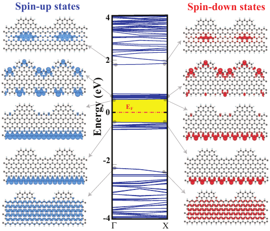
Earlier, it was shown that the edge roughness of graphene NRs can affect their electronicGunlycke ; Yoon ; Evaldsson and mechanicalcan-mechanical properties. In particular, it was revealed that periodically repeating edge profiles can be treated within the superlattice structure, which result in confinement of spin states in zigzag NRs.haldun-super Band alignments of these superlattice structures have been studied both experimentally and theoretically.dai Here we investigated the effect of periodically repeating edge roughness of a bare zigzag graphane NR. While one edge of NR is kept flat, periodically repeating undulations are carved at the other edge. The same structure can be viewed as periodically repeating heterostructures of wide (=8) and narrow (=6) segments of zigzag graphane NRs. Atomic and electronic band structure of this superlattice, which mimics the edge roughness are shown in Fig. 7. Here we note that infinite bare zigzag graphane NR with =8 has a band gap of 0.8 eV, while the band gap of infinite bare zigzag graphane NR with =6 is relatively wider and 0.9 eV. As pointed out in Sec. IV, wide band gap of H-passivated graphane NRs is reduced to 0.8-0.9 eV because of edge states of unpassivated dangling bonds of bare graphane NRs, which appear in the band gap. These edge states in Fig. 7 of the superlattice occur as several closely lying flat bands below and above the Fermi level separated by a superlattice band gap of 0.8 eV. The character of various bands are revealed by plotting the charge density isosurfaces of various states. Charge density isosurfaces of the highest filled spin up and spin down edge state indicate the localization at the flat edge. As for the charge distribution of the lower lying valence states is rather uniform along the narrow region. The states of the flat band at the edge of the conduction band is confined in the wide segment of the superlattice since they cannot find a matching state in the narrow region. As a proof of the concept, it is shown that electronic states can be confined at specific regions of periodic edge roughness. Of course, confinement, superlattice band gap etc. depend on the structural parameters of superlattices and need detailed investigation.
VIII Discussions and Conclusions
Research on recently synthesized graphane revealed interesting electronic and magnetic properties of this two dimensional honeycomb structure. Graphane attains a -like bonding through covering of its both sides by hydrogen atom. This bonding is rather different from the -bonding of graphene and attributes a number of additional properties to graphane. For example, in contrast to semimetallic graphene with linear band crossing at the Fermi level, graphane is a nonmagnetic, wide band semiconductor.
The armchair and zigzag graphane NRs of graphane display important number of properties and hence constitute basic structures to fabricate various devices. Both zigzag and armchair graphane NRs are wide band gap semiconductor when their edges are passivated with hydrogen. The band gaps vary exponentially with their widths. For narrow graphane NRs the band gap is large due to quantum confinement effect, but approaches to the band gap of graphane as the width increases. Unpaired, unpassivated dangling bonds at the edges have 1 Bohr magneton magnetic moment and have antiferromagnetic coupling with adjacent dangling bonds. These graphane NRs can be functionalized to attain additional properties through H-passivation of their edges, adatom adsorption, vacancy creation, edge profiling and superlattice formation. In particular, graphane NRs attain magnetic moment through the creation of H vacancy at the surfaces of graphane. This property can be utilized to achieve interesting functionalities through decoration and patterning of H-vacancies on the graphane NRs. The possibility of generation of large magnetic moments at small domains of H-vacancies makes graphane based structures promising for data storage and nanospintronic applications. These functionalities can be further extended by adsorbing adatoms to carbon atoms deprived from hydrogen.
In conclusion, the present study demonstrates that graphane NRs can be an important basic nanomaterial and presents interesting properties for future technological applications.
Acknowledgements.
Computing resources used in this work were partly provided by the National Center for High Performance Computing of Turkey (UYBHM) under grant number 2-024-2007. This work is partially supported by the project of The State Planning Organization (DPT) of Turkey and by Academy of Science of Turkey (TÜBA).References
- (1) K. S. Novoselov, D. Jiang, F. Schedin, T. J. Booth, V. V. Khotkevich, S. V. Morozov, and A. K. Geim, Science 306, 666 (2004).
- (2) K. S. Novoselov, A. K. Geim, S. V. Morozov, D. Jiang, M. I. Katsnelson, I. V. Grigorieva, S. V. Dubonos, and A. A. Firsov, Nature (London) 438, 197 (2005).
- (3) Y. Zhang, Y.-W. Tan, H. L. Stormer, and Philip Kim, Nature (London) 438, 201 (2005).
- (4) C. Berger, Z. Song, X. Li, X. Wu, N. Brown, C. Naud, D. Mayou, T. Li, J. Hass, A. N. Marchenkov, E. H. Conrad, P. N. First, and W. A. de Heer, Science 312, 1191 (2006).
- (5) M. I. Katsnelson, K. S. Novoselov, and A. K. Geim, Nat. Phys. 2, 620 (2006).
- (6) A. K. Geim and K. S. Novoselov, Nature Mat. 6, 183 (2007).
- (7) M. Y. Han, B. Özyilmaz, Y. Zhang, and P. Kim, Phys. Rev. Lett. 98, 206805 (2007).
- (8) X. Li, X. Wang, L. Zhang, S. Lee, and H. Dai, Science 319, 1229 (2008).
- (9) H. Lee, Y. W. Son, N. Park, S. Han, and J. Yu, Phys. Rev. B 72, 174431 (2005).
- (10) V. Barone, O. Hod, and G. E. Scuseria, Nano Lett. 6, 2748 (2006).
- (11) D. A. Abanin, P. A. Lee, and L. S. Levitov, Phys. Rev. Lett. 96, 176803 (2006).
- (12) A. Cresti, G. Grosso, and G. P. Parravicini, Phys. Rev. B 76, 205433 (2007).
- (13) M. Ezawa, Phys. Rev. B 73, 045432 (2006).
- (14) J. Guo, D. Gunlycke, and C. T. White, Appl. Phys. Lett. 92, 163109 (2008).
- (15) O. Hod, V. Barone, J. E. Peralta, and G. E. Scuseria, Nano Lett. 7, 2295 (2007).
- (16) D. C. Elias, R. R. Nair, T. M. G. Mohiuddin, S. V. Morozov, P. Blake, M. P. Halsall, A. C. Ferrari, D. W. Boukhvalov, M. I. Katsnelson, A. K. Geim and K. S. Novoselov, Science 323, 610 (2009).
- (17) J. O. Sofo, A. S. Chaudhari and G. D. Barber, Phys. Rev. B 75, 153401 (2007).
- (18) D. W. Boukhvalov, M. I. Katsnelson and A. I. Lichtenstein, Phys. Rev. B 77, 035427 (2008).
- (19) M. Z. S. Flores, P. A. S. Autreto, S. B. Legoas and D. S. Galvao , Nanotechnology 20, 465704 (2009).
- (20) Y. Li, Z. Zhou, P. Shen and Z. Chen, J. Phys. Chem. C 113, 15043 (2009).
- (21) H. Şahin, C. Ataca and S. Ciraci, Appl. Phys. Lett. 95, 222510 (2009).
- (22) S. Lebegue, M. Klintenberg, O. Eriksson, and M. I. Katsnelson, Phys. Rev. B 79, 245117 (2009).
- (23) G. Kresse and J. Hafner, Phys. Rev. B 47, 558 (1993); G. Kresse and J. Furthmüller, Phys. Rev. B 54, 11169 (1996).
- (24) P. E. Blochl, Phys. Rev. B 50, 17953 (1994).
- (25) D. M. Ceperley and B. J. Alder, Phys. Rev. Lett. 45, 566, (1980).
- (26) M. Shishkin and G. Kresse, Phys. Rev. B 74, 035101 (2006).
- (27) M. R. Sorensen, M. Brandbyge, and Karsten W. Jacobsen, Phys. Rev. B 57, 57, 3283 (1998).
- (28) H. Şahin, S. Cahangirov, M. Topsakal, E. Bekaroglu, E. Aktürk, R. T. Senger, and S. Ciraci, Phys. Rev. B 80, 155453 (2009).
- (29) C. Lee, X. Wei, J. W. Kysar, and J. Hone, Science 321, 385 (2008).
- (30) M. Topsakal, S. Cahangirov, and S. Ciraci, Appl. Phys. Lett. 96, 091912 (2010).
- (31) H. Lee, Y. W. Son, N. Park, S. Han, and J. Yu, Phys. Rev. B 72, 174431 (2005).
- (32) H. Şahin and R. T. Senger, Phys. Rev. B 78, 205423 (2008).
- (33) C. Ataca, E. Aktürk, and S. Ciraci, Phys. Rev. B 79, 041406(R) (2009).
- (34) K. T. Chan, J. B. Neaton, and M. L. Cohen, Phys. Rev. B 77, 235430 (2008).
- (35) Z. Liu, L. C. Feldman, N. H. Tolk, Z. Zhang, and P. I. Cohen, Science 312, 1024 (2006).
- (36) L. Breaux, B. Anthony, T. Hsu, S. Banerjee, and A. Tasch, Appl. Phys. Lett. 55, 1885 (1989).
- (37) S. Vajda, M. J. Pellin, J. P. Greeley, C. L. Marshall, L. A. Curtiss, G. A. Ballentine, J. W. Elam, S. Catillon-Mucherie, P. C. Redfern, F. Mehmood, and P. Zapol, Nature Mat. 8, 213 (2009).
- (38) E. H. Lieb, Phys. Rev. Lett. 62, 1201 (1989).
- (39) B. S. Pujari and D. G. Kanhere, J. Phys. Chem. C 113, 21063 (2009).
- (40) D. Gunlycke, D. A. Areshkin, and C. T. White, Appl. Phys. Lett. 90, 142104 (2007).
- (41) Y. Yoon, and J. Guo, Appl. Phys. Lett. 91, 073103 (2007).
- (42) M. Evaldsson, I. V. Zozoulenko, H. Xu, and T. Heinzel, Phys. Rev. B 78, 161407(R) (2008).
- (43) H. Şahin, C. Ataca and S. Ciraci (Unpublished).
- (44) H. Sevinçli, M. Topsakal, and S. Ciraci, Phys. Rev. B 78, 245402 (2008).
- (45) X. Li, L. Zhang, S. Lee, and H. Dai, Science 319, 1229 (2008).