Design and optimization of plasmonic-based metal-dielectric nanocomposite materials for energy applications
Abstract
Metallic nanoparticles embedded in dielectrics permit enhanced capture of light at specific wavelengths through excitation of plasmons, i.e. the quanta of coherent and collective oscillations of large concentrations of nearly free electrons. In order to maximize the potential of such enhanced absorption in useful tasks, such as the generation of carriers in photocatalysts and semiconductors, it is important to be able to predict and design plasmonic nanocomposites with desired wavelength-dependent optical absorption. Recently, a mixing approach formulated by Garcia and co-workers [Phys. Rev. B, 75, 045439 (2007)] has been successfully applied to model the experimentally measured broadband optical absorption for ternary nanocomposites containing alloys or mixtures of two metals (from Ag, Au or Cu) in SiO dielectric. In this work we present the broadband optical behavior of important optical coating dielectrics (SiN and SiO) and photocatalyst (TiO) containing various configuration of nanoparticles of Al, Au, Ag, or Cu. The spectral behavior of various combinations of the metallic species in the dielectrics was optimized to show either broadband solar absorption or strong multiple plasmonic absorption peaks. The applications of such nanocomposite materials in solar energy harvesting and spectral sensing are also presented and discussed.
1Department of Physics, Washington University, St. Louis, Missouri 63130, USA;
2Center for Materials Innovation, Washington University, St. Louis, Missouri 63130, USA;
3Department of Physics, Southern Illinois University, Edwardsville, Illinois 62026, USA;
Department of Biomedical and Chemical Engineering, Syracuse, NY 13203
5Materials Science and Engineering, University of Tennessee, Knoxville 37996, USA
6Chemical and Biomolecular Engineering, University of Tennessee, Knoxville 37996, USA
1 Introduction
The strong optical interaction seen when nanoscale metal-dielectric structures interact with light promise several applications, including optical manipulation well below the diffraction limit, high-speed information processing and integration of Si electronics with optics [1, 2, 3, 4]. The strong interaction is a result of the resonant absorption of electromagnetic radiation by plasmons, which are collective oscillations of large concentrations of nearly free electrons [5]. For nanoscale metallic structures, surface plasmons are primarily responsible for this interaction. Nanocomposites made from metal nanostructures embedded in or placed on dielectrics offer significant potential as materials showing enhanced or tunable light harnessing [6, 7, 8, 9]. For instance, Schaadt and co-workers [7] have shown that incorporation of Au nanoparticles on the surface of a Si photodiode results in enhanced photocurrent at specific wavelengths that were correlated to the surface plasmon resonance. However, the fabrication of practically useful devices that utilize plasmonics to achieve a desired optical and/or electronic response requires the careful design and fabrication of nanomaterials with well defined shape, size and metal-dielectric composition. Recently, there has been tremendous activity in controlling the physical attributes of nanoscale metallic structures, such as the particle size and shape, through a variety of techniques, including ion irradiation [10, 11, 12, 13], laser-assisted chemical vapor decomposition [14, 15] and laser-induced dewetting [16, 17, 18, 19]. However, the fabrication of metal-dielectric nanocomposites driven by a knowledge-based design of optical properties is very important towards realizing cost-effective means for manufacturing such novel materials.
In this work we focus on a theory-driven design and optimization of metal-dielectric nanocomposites that can show broadband optical absorption via plasmonic effects. The desire to achieve broadband plasmonic absorption comes from the various experimental results that show that nanoparticles and nanocomposite coatings on photovoltaic devices can give rise to a wavelength-dependent photocurrent enhancement that correlates to the plasmonic responses of the applied material [7, 20, 8, 6]. While consideration of the effects of electromagnetic scattering due to the absorbing-layer’s microstructure leads to further optimization [20, 21], optimizing the absorption of incident solar energy though judicious design of metal type, nanoparticle shape, its volume fraction, and the host dielectric [22, 23, 24, 6] is likely to be the first step to an improved device. Recently, a homogenization procedure has been proposed using the tight lower bounds of the Bergman-Milton formulations to characterize the optical properties of ternary nanocomposites consisting of metallic nanoparticles embedded in various host dielectrics [25]. Using this model, excellent agreement was found between the experimentally measured and theoretically estimated optical absorption for a variety of plasmonic systems, including binary alloys, mixtures and core-shell structures. Based on this success, we have extended the mixing approach and applied it to the case of quaternary metal-SiO nanocomposites, i.e. a system containing three different metals in SiO, to predict the broadband spectral response. We showed that a judicious selection of metal type, their concentration and particle size can result in broadband plasmonic light absorption [26], a feature that could be very beneficial in applications that need to maximize the absorption of incident broadband solar radiation, such as in solar cells and photodetectors .
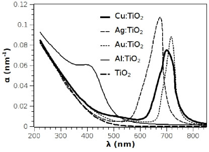
Here we present calculations of the broadband optical properties of other useful dielectric material, including Si3N4 and TiO. SiN is used in conventional solar cell technology as an anti-reflective coating layer [27]. We have calculated the optical properties of binary and quaternary nanocomposites (NC) made from different metals (Al, Cu, Ag, Au) in SiN and determined wavelength regimes of strong absorption. Based on these results we have designed a broadband absorbing nanocomposite whose absorption spectra is optimized to match the shape of the 1.5 AM incident solar radiation. Our results show that a quaternary NC containing Cu, Ag and Al in SiN shows extremely good broadband absorption spectra. In comparison, similar broadband absorption in SiO requires Cu, Ag and Au nanoparticles. TiO2 is an essential component in dye-sensitized solar cells [28] and its photocatalytic properties have a variety of uses, including in paint, in self-cleaning glasses, and in multifunctional coatings [29]. However, one of the outstanding challenges in TiO is to enhance its absorption in the visible spectrum. Towards this goal, we have explored the plasmonic absorption of several different metals (Al, Cu, Ag, Au) in TiO. Our calculations show that strong absorption occurs in the range of 670-700 nm by Cu, Ag or Au while Al shows broad absorption from the UV into the visible till about 500 nm. The results of this work show that it is possible to design and optimize the optical behavior of metal-dielectric nanocomposites with desired optical response, including for applications in energy harvesting. The remainder of this paper is divided as follows. In Sec. 2 we discuss the basic ideas behind plasmonics and plasmonic absorption and present the homogenization scheme that permits a theoretical estimate of the optical absorption in multimetal-dielectric nanocomposites. In Sec. 3 we discuss potential applications resulting from NCs that show absorption in broadband and/or at specific wavelengths. We also discuss the computational optimization scheme based on the simulated annealing technique that permits the optimization of a nanocomposite. We conclude the paper with brief discussions in Sec. 4.
2 Homogenization Scheme
The essential physics of the plasmonic properties of metals irradiated by electromagnetic radiation in the optical regime are captured by the Drude-Sommerfeld theory of metals, with corrections to the kinetics of the free electron Fermi gas due to energetic contributions from bound electrons [30]. When a collection of atoms are brought together forming a crystalline lattice, one must determine the energy states of the system of valence electrons as their motion is influenced by the lattice ions and mutual interaction. In practice, the wave functions of the valence electrons are not strongly concentrated about their original atomic position but spread wide through the metal with a distance comparable to the mean-free path of the electrons ( angstroms). Hence, the valence electrons form a sea filling the various electronic states of the system as a whole [31]. A plasma oscillation in a metal is a collection of longitudinal or transverse excitation of these free electrons. A plasmon refers to the quanta of such an oscillation which may be stimulated by an incident electromagnetic (EM) wave. Preferential coupling between an incident EM wave and a particular plasmon mode can give rise to resonance phenomenon. At normal incidence, for EM wavelengths corresponding to this resonance frequency, the momentum of the plasmon will be negligible because the momentum of the reflected photon is virtually zero. Thus, excitation of the plasmon mode is localized at the surface of the medium. However, for certain angles, when requirements for energy and momentum conservation are met, a surface-plasmon polariton wave may be induced that propagates along the surface of the media. The existence of these self-sustaining collective excitations at metal surfaces was originally predicted by Ritchie [32].For the case of metallic nanoparticles, surface plasmonic effects are the dominate mechanism dictating the interaction with EM energy. When metallic nanoparticles are embedded in a host dielectric, the precise wavelength where EM energy and plasmonic modes couple at metal-film interface is dictated by the dielectric coefficient for the individual phases. The essential physics of this charge oscillation for dilute systems of metal nanoparticles () in a dielectric matrix is captured by the lower bound for the effective dielectric coefficient proposed by Bruggeman [33] and Milton [34]. We have taken the binary dielectric mixing rule from Bruggeman and Milton and extended its application to multi-metal nanocomposite systems via a homogenization technique [25].
In the limit of long electromagnetic wavelength relative to the system microstructure, the technique of homogenization, where two or more constituent phases are blended together in such a manner that the resulting composite material appears as a continuous material, is an important tool in characterising the desired macroscopic responses of engineered materials. A large amount of research is dedicated towards placing bounds on the maximum and minimum values of the macroscopic dielectric coefficient that composite materials may take when only limited information is provided on features of the constituent phases including: volume fraction, average spacing, and/or spatial distribution [35, 36, 33, 34, 37]. Such models have been used in geological applications and are useful in predicting the behavior of natural occurring composites such as reservoir rocks [35] or ice [37], which may contain dilute concentrations of useful resources such as natural gas, water, or minerals. While many bounds are available in the literature, certain bounds are more useful towards narrowing down the range of predicted macroscopic behavior for a particular situation of interest [37]. For example, the Wiener bounds are the loosest, giving the maximum and minimum values of the effective dielectric function independent of the type of mixture in question. For systems that are isotropic and with uniformly distributed constituents, the Hashin-Shtrikman bounds, based on a variational formulation of the energy functional for the mixture, represents a tighter range of values than the Weiner bounds at the expense of the added assumptions [38]. In addition to the Hashin-Shtrikman approach, two other widely circulated bounds in the literature are the Maxwell-Garnett and Bruggeman formalisms [39]. However, these tighter approaches do not necessarily yield physically realistic estimates in certain parameter regimes [40]. Recently we have shown that a homogenization procedure based on the tight lower bound given by Bergman and Milton [36, 34] is able to predict optical data in dilute nanocomposite materials without the use of any fitting parameters [25]. In this procedure, the effective dielectric function for a binary metal-dielectric composite can be expressed as follows:
| (1) |
where denotes the component’s volume fraction, is the component’s dielectric function depending on the wavelength of the incident electromagnetic energy with subscripts and referencing the metal and host matrix respectively. is a geometrical factor taking into account the shape of the metal particles which may posses spatial dependence for non-symmetric inclusion geometries [37]. For the purposes of this paper we are interested in spherical particles and accordingly choose . Here, we also assume the spherical inclusions are distributed with enough uniformity in the host matrix that system spatial dependence may also be neglected. Equation 1 represents the effective dielectric function for the two component case of a metal particle embedded in a host dielectric matrix. Note it is customary to let where corresponds to the metal components [37]. Our analysis made use of experimentally measured optical data from Ref. [41]. In Fig. 1 the effective absorption coefficient , given by
| (2) |
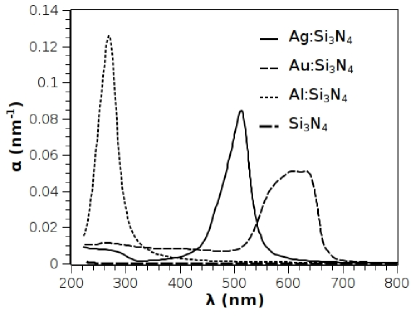
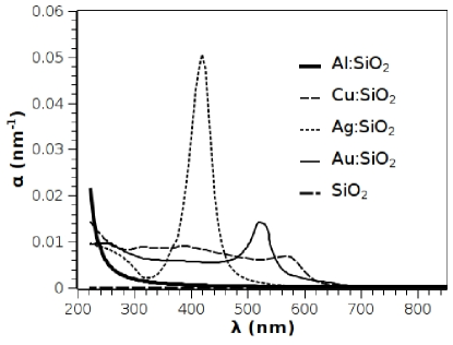
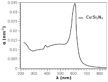
where is the wavelength of incident electromagnetic energy, of a single metal species () embedded in a Si3N4, TiO2, or SiO2 matrix is presented. For the case of Al, Au, and Ag nanoparticles in Si3N4, the composite system possesses a vary sharp increase in absorption localize about a particular wavelength ( nm, nm, and nm for Al, Ag, and Au respectively) (Fig. 1a). Similar behavior is observed for Au, Ag, and Cu (Fig. 1d) nanoparticles embedded in TiO2 with localized absorption enhancements nm, nm, and nm respectively, all corresponding to photons with energies below the bandgap of TiO2 (3.0 eV). Similarly, Ag and Au in SiO2 also exhibit strong absorption near their plasmonic responses with respective absorption enhancements in the vicinity of 414 nm and 529 nm, respectively (Fig. 1b). Al in SiO2 shows strong absorption in the UV near the edge of the available experimental data (Fig. 1b). However, Cu inclusions in Si3N4 and SiO2 exhibit a broadband response spanning from the UV to the visible regime (Figs. 1b and 1c). Near 640 nm Cu in Si3N4 possesses a very strong absorption enhancement. It is of interest to note that the resonance response of Cu, Au, and Ag in Si3N4 all correspond to photon energies below the bandgap of Si3N4 (4.5 eV). In addition, Al in TiO2 exhibits a broader response than the other presented metals embedded TiO2 with an absorption enhancement ranging from the UV to a wavelength nm (Fig. 1d). In Fig. 1(a), 1(b), and 1(d) the absorption spectrum of the dielectric material with no metal inclusions is also shown for comparison purposes. Note that the presence of metal nanoparticles greatly enhances the absorption predicted from that of the standalone dielectric matrix.
We now discuss the optical behavior of dielectric containing nanoparticles of multiple different metals. For the systems considered here, the analysis is limited to the dilute case (i.e. total volume fraction of metal versus dielectric ) because it is desirable from a practical standpoint of expense and fabrication efficiency. An additional constraint we have placed is to set the minimum nanosphere diameter to be no less than nm. Above this size regime, exotic quantum confinement effects may be neglected [42]. Furthermore, nanoparticles of size 10 nm can be assembled on many dielectric substrates using robust manufacturing techniques such as those mentioned in the introduction. Figures illustrating the hierarchical mixing process for both 2- and 3-metal mixtures have been presented elsewhere [25, 26]. The top level represents the effective dielectric function for the target nanocomposite of design interest. At each level, the total volume fraction is constrained such that . During the mixing process, the average electric field within the composite is held constant while the final effective permittivity is calculated using equal volumes at each level of mixing. As described in Ref. [25]: the effective permittivity of an N-component mixture can be determined by mixing N-1 binary mixtures, each comprising of a host and a distinct metal, the host being common to the N-1 pairs.
At the plasmonic resonance, the absorption is not infinite in extent and broadened absorption lines are observed due to the finite relaxation times of scattering [43]. For the case of spherical metal particles of nanometer extent, finite size corrections are introduce through modification of the imaginary portion of the effective dielectric coefficient. Eq. 3 quantifies the effective change in the electron relaxation time due to scattering of electrons on the metal-dielectric interface as a slight modification to the bulk electron relaxation time [44] expressed by :
| (3) |
where is the effective electron relaxation time, is the bulk electron relaxation time, corresponds to the particle’s diameter and is the velocity of the electrons near the Fermi surface. The values of and for the various metals examined in this study were taken from Ref. [30]. The size effect may be incorporated in the mixing approach though modification of the imaginary portion of the effective dielectric coefficient [25] as follows
3 Potential Applications and Optimization Scheme
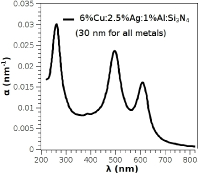
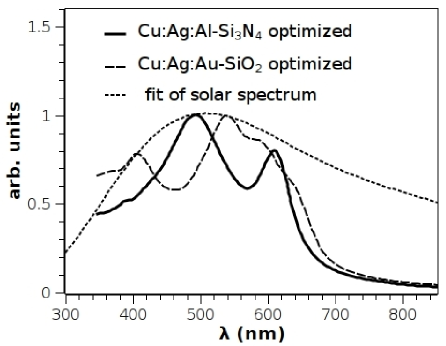
In Fig. 2, the optical absorption response obtained by the mixing approach are presented with specific applications in consideration. We begin by noting that it has been previously shown that an absorbing layer on a photovoltaic device can exhibit photocurrent enhancement correlating with the plasmonic responses of the layer [7, 45]. This motivates the application discussion here. Fig. 2(a) presents a system configuration where the spectral response is broadband with absorption peaks at 264 nm, 496 nm, and 609 nm due to the respective interaction of Al, Ag, and Cu with Si3N4. The chosen configuration (6.0% Cu, 2.5% Ag, and 1.5% Al with all spherical inclusions possessing a diameter of 30 nm) causes the maximum of the peaks to occur at different locations over the spectral range. While optimizing the size and concentration can result in several different absorption profiles [26], Fig. 2(a) illustrates an important design example, i.e. one in which absorption can be simultaneously maximized at several different and specific wavelengths. In Fig. 2(b) we present the design solution for a Cu:Ag:Al-Si3N4 nanocomposite whose absorption coefficient is optimized to resemble the shape of the incident solar spectrum (1.5 AM) using a simulated annealing algorithm [46, 47, 48]. We define the “energy” to be minimized as with composite parameters and . and represent the normalized solar spectrum data [49] and effective nanocomposite absorption at a given wavelength respectively. We define this “energy” for spanning from 200 to 900 nm. This choice of allows for the absorption profile that most closely resembles the shape of the solar spectrum to be determined. The algorithm begins by initializing the system to some initial state . A neighboring state is called by using the condition
| (5) |
where with being a vector of dimension with each component taking a random value between . represents the maximum magnitude the volume fraction of a particular species may step. Similarly, with representing the maximum magnitude the diameter of the particles corresponding to a particular species may step. Here, values of and nm provided sufficient finesse in moving through the search space. Next, the neighboring state is compared with the best state encountered thus far (where was originally initialized to the same state as ). If then is set equal to . Then, the algorithm must decide if this neighbor state will become the preferred state for the system. To accomplish this, a Boltzmann-type probability analogous to classical statistical physics is calculated– namely
| (6) |
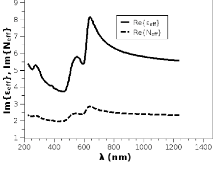
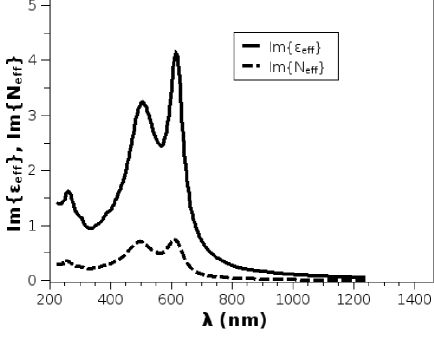
where is the annealing parameter analogous to temperature and is a constant used to refine the annealing schedule. Note that if then is simply reassigned to 1. is then compared to a random number between . If then is accepted as the new system state and . Notice from Eq. 6 that if , then the neighboring state is always accepted as the new system state. The process of calling neighbor states and deciding whether or not to accept them as system state is repeated over cycles. This represents a random walk of -steps through the parameter space. For optimization calculations performed here, was chosen to be as for values greater than this no appreciable difference in the results was observed. At each iteration of the algorithm, only values in the dilute regime and outside the realm of quantum effects were accepted (i.e. and nm were enforced at each step). In addition, the maximum particle size was constrained to nm as mentioned above and only physically realizable values of volume fractions were permitted (). If the algorithm suggested a neighbor state outside the allowable domain, a large value was assigned to the energy (). This, by virtue of Eq. 6, gives a very low probability for such states to be accepted. Finally, is reduced and the entire process repeated again. is reduced according to a prescribed schedule until it is nearly equal to zero after iterations. Notice that as is slowly reduced the system begins to accept lower and lower energy configurations until the it is forced to into a (global) minimum. For calculations conducted here, the annealing schedule prescribed was where using iterations. The initial value of was chosen so that the probability of the algorithm proceeding from a lower state to a higher state and vice versa was approximately the same. This ensured that the search space was relatively large during the initial stages of the anneal. A value of with was used for simulations here. Typically, and was taken as an initial guess. When numerical parameters were determined such that different simulation runs yielded the same answer (within a tolerance of ), different initial states where chosen and simulations ran again. This was done to verify that the algorithm had, in fact, determined the system configuration yielding the global minimum. The optimum configuration was determined to be 5.45% Cu, 0.421% Al, and 4.11% Ag in Si3N4 with respective nanosphere diameters of 30 nm, 22.27 nm, and 10.0 nm. The spectral response is show in Fig. 2b. We note that configurations of this type do exhibit some enhancement to the complex index of refraction () as compared to the index of the refraction of the stand-alone Si3N4 matrix (e.g., Figs. 3(a) and 3(b) present the real and imaginary portions of and for a Cu:Al:Ag in Si3N4 nanocomposite system respectively), leading to enhanced reflectivity at this wavelengths lessening the enhancement of the increased absorption. However, it is common practice to compensate for this effect by introducing an anti-reflection layer on top of the solar absorption coating [45]. Similarly, the data for an optimized quaternary nanocomposite of Cu:Ag:Au-SiO2 from [26] is presented in Fig. 2(b). The optimal configuration determined in that study was 1.80% Cu, 0.35% Ag, and 6.40% Au with respective particle diameters of 10.1 nm, 29.6 nm and 10.0 nm. Both absorbing layers may have applications in enhancing the photocurrent of existing photovoltaic devices.
4 Conclusions and Discussion
Here we have applied the mixing rule developed by Garcia and co-workers [25] to model the composite electromagnetic behavior for configurations of Al, Au, Ag, and Cu metallic nanospheres embedded in dielectric hosts consisting of Si3N4, TiO2, and SiO2. The presence of metal nanoparticles greatly enhances the absorption spectrum predicted from that of the standalone dielectric matrix. Certain combinations of metal and nanoparticle concentrations exhibited a broadband response (e.g. Cu in Si3N4, Al in TiO2, and Cu in SiO2 ) while strong localized absorption was predicted for other systems (e.g. Ag in all mentioned host dielectrics). Of note, the resonance absorption enhancement predicted for Au, Ag, and Cu in Si3N4 and TiO2 all correspond to photon energies below the respective bandgaps of the host dielectric ( 4.5 eV for Si3N4 and 3.0 eV for TiO2). Such interaction may have application in carrier generation for the next generation of photocatalysis and semiconductor devices. In addition, potential uses for spectral sensing and an optimization approach to find preferential system combinations for solar energy harvesting have been presented and discussed. The use of such nanocomposite systems as absorbing layers on photovoltaic devices adds another degree of freedom for device tailoring and potential efficiency enhancement. Consideration of the stability of such embedded nanoparticle systems under various processing conditions and the steps towards fabrication of nanocomposites of the type described are currently under investigation.
RK, and RS acknowledge support by the National Science Foundation through grants # CMMI-0855949, while HG acknowledges support by the National Science Foundation through grant # CMMI-0757547.
References
- [1] H. Atwater, The Promise of Plasmonics, Scientific American 4 (2007) 56–63.
- [2] M. Quinten, A. Leitner, J. Krenn, F. Aussenegg, Electromagnetic energy transport via linear chains of silver nanoparticles, Optics Lett. 23 (17) (1998) 1331–33.
- [3] J. Krenn, J. C. Weeber, A. Dereux, B. Schider, A. Leitner, F. R. Aussenegg, C. Girard, Direct observation of localized surface plasmon coupling, Phys. Rev. B 60 (1999) 5029–5033.
- [4] U. Fischer, A. Dereux, J.-C. Weeber, Near-field optics and surface plasmon polaritons, Vol. 81 of Topics in applied physics, Springer, 2001, Ch. Controlling light confinement by excitation of localized surface plasmons, pp. 49–69.
- [5] C. Kittel, Introduction to solid state physics, 7th ed., John Wiley and Sons, Ltd., New York, 2003.
- [6] H. Stuart, D. Hall, Island size effects in nanoparticle-enhanced photodectors, App. Phys. Lett. 73 (26) (1998) 3815–17.
- [7] D. Schaadt, B. Feng, E. Yu, Enhanced semiconductor optical absorption via surface plasmon excitation, App. Phys. Lett. 86 (2005) 063106.
- [8] S. Pillai, K. Catchpole, T. Trupke, G. Zhang, J. Zhao, M. Green, Enhanced emission from Si-based light-emitting diodes using surface plasmons, App. Phys. Lett. 88 (2006) 161102.
- [9] J. Cole, N. Halas, Optimized plasmonic nanoparticle distributions for solar spectrum harvesting, App. Phys. Lett. 89 (2006) 153120.
- [10] Y. Mishra, D. Avasthi, P. Kulriya, F. Singh, D. Kabiraj, A. Tripathi, J. Pivin, I. Bayer, A. Biswas, Controlled growth of gold nanoparticles induced by ion irradiation: An in situ x-ray diffraction study, App. Phys. Lett. 90 (2007) 073110.
- [11] G. Battaglin, E. Cattaruzza, F. Gonella, G. Mattei, P. Mazzoldi, C. Sada, X. Zhang, Formation of metal-alloy nanoclusters in silica by ion implantation and annealing in selected atmosphere, Nuc. Instr. Met. Phys. Res. B 166-167 (2000) 857–863.
- [12] R. H. Magruder III, D. H. Osborne Jr., R. A. Zuhr, Non-linear optical properties of nanometer dimension Ag-Cu particles in silica formed by sequential ion implantation, J. Non-Cryst. Sol. 176 (1994) 299–303.
- [13] A. Meldrum, L. A. Boatner, C. W. White, Nanocomposites formed by ion implantation: Recent developments and future opportunities, Nuc. Instr. Meth. Phys. Res. B 178 (2001) 7–16.
- [14] K. Elihn, L. Landstrom, O. Alm, M. Boman, P. Heszler, Size and structure of nanoparticles formed via ultraviolet photolysis of ferrocene, J. App. Phys. 101 (2007) 034311.
- [15] K. Elihn, F. Otten, M. Boman, P. Heszler, F. Kruis, H. Fissan, J.-O. Carlsson, Appl. Phys. A.: Mater. Sci. Process. 72 (2001) 29.
- [16] J. Trice, D. Thomas, C. Favazza, R. Sureshkumar, R. Kalyanaraman, Investigation of pulsed laser induced dewetting in nanoscopic metal films: Thermal modeling and experiments, Phys. Rev. B 75 (2007) 235439.
- [17] A. K. Gangopadhyay, H. Krishna, C. Favazza, C. Miller, R. Kalyanaraman, Heterogeneous nucleation of amorphouse alloys on catalytic nanoparticles to produce 2D patterned nanocrystal arrays, Nanotechnology 18 (2007) 485606.
- [18] C. Favazza, R. Kalyanaraman, R. Sureshkumar, Robust nanopatterning by laser-induced dewetting of metal nanofilms, Nanotechnology 17 (2006) 4229–4234.
- [19] C. Favazza, J. Trice, H. Krishna, R. Sureshkumar, R. Kalyanaraman, Laser induced short and long-range ordering of Co nanoparticles on SiO2, Appl. Phys. Lett. 88 (2006) 153118–1–3.
- [20] D. Derkacs, S. Lim, P. Matheu, W. Mar, E. Yu, Improved performance of amorphous silicon solar cells via scattering from surface plasmon polaritons in nearby metallic nanoparticles, App. Phys. Lett. 89 (2006) 093103.
- [21] S. Pillai, K. Catchpole, T. Trupke, M. Green, Surface plasmon enhanced silicon solar cells, J. App. Phys. 101 (2007) 093105.
- [22] J. Zhang, H. Liu, Z. Wang, N. Ming, Synthesis of gold regular octahedra with controlled size and plasmon resonance, App. Phys. Lett. 90 (2007) 163122.
- [23] L. Douillard, F. Charra, C. Fiorini, Optical properties of metal nanoparticles as probed by photoemission electron microscopy, J. App. Phys. 101 (2007) 083518.
- [24] Y. Su, W. Lai, W. Chen, M. Hon, S. Chang, Surface plasmon resonance of gold nano-sea-urchin, App. Phys. Lett. 90 (2007) 181905.
- [25] H. Garcia, J. Trice, R. Kalyanaraman, R. Sureshkumar, Self-consistant determination of plasmonic resonances in ternary nanocomposites, Phys. Rev. B 75 (2007) 0405439.
- [26] J. Trice, H. Garcia, R. Sureshkumar, R. Kalyanaraman, In silico design of metal-dielectric nanocomposites for solar energy applications, in: Instrumentation, Metrology, and Standards for Nanomanufacturing., Vol. 6648 of Proc. SPIE, 2007, pp. 66480L–1.
- [27] B. Sopori, Silicon Nitride Processing for Control of Optical and Electronic Properties of Silicon Solar Cells, J. Elec. Mat. 32 (10) (2003) 1034.
- [28] M. Gratzel, B. O’Regan, A low-cost, high-efficiency cell based on dye-sensitized solar cell based on dye-sensitized colloidal TiO2 films, Nat. 353 (1991) 737.
- [29] L. A. Brook, P. Evans, H. A. Foster, M. E. Pemble, D. Sheel, A. Steele, H. Yates, Novel multifunctional films, Surf. Coat. Tech. 201 (2007) 9373.
- [30] N. Ashcroft, D. Mermin, Solid State Physics, Holt, Rinehart, and Winston, 1976.
- [31] J. M. Ziman, Electrons and Phonons: The Theory of Transport Phenomena in Solids, Oxford University Press, Oxford, 1960.
- [32] R. H. Ritchie, Plasma Losses by fast electrons in Thin Films, Phys. Rev. 106 (1957) 874.
- [33] D. Bergman, Bounds for the complex dielectric constant of a two-component composite material, Phys. Rev. B. 23 (6) (1981) 3058–3065.
- [34] G. W. Milton, J. App. Phys. 52 (1981) 5286.
- [35] L. C. Shen, C. Liu, J. Korringa, K. J. Dunn, Computation of conductivity and dielectric constant of periodic porous media, J. Appl. Phys. 67 (1990) 7071.
- [36] D. J. Bergman, Phys. Rev. Lett. 44 (1980) 1285.
- [37] A. Sihvola, Electromagnetic mixing formulas and applications, The Institution of Electrical Engineers, London, UK., 1999.
- [38] K. K. Karkkainen, A. H. Sihvola, K. I. Nikoskinen, Effective Permittivity of Mixtures: Numerical Validation by the FDTD Method, IEEE Trans. Geosci. Re. Sens. 38 (3) (2000) 1303.
- [39] A. J. Duncan, T. G. Mackay, L. Akhlesh, On the Bergman-Milton bounds for the homogenization of dielectric composite materials, Opt. Comm. 271 (2007) 470–474.
- [40] T. Mackay, Opt. Commun. 234 (2004) 35.
- [41] SOPRA database, http://www.sopra-sa.com/ (2006).
- [42] W. P. Halperin, Rev. Mod. Phys. 58 (1986) 533.
- [43] J. M. Ziman, Principles of The Theory of Solids, 2nd ed., Cambridge University Press, Cambridge, 1972.
- [44] L. Yang, D. H. Osborne, R. F. Haglund, Jr., R. H. Magruder, C. W. White, R. A. Zuhr, H. Hosono, Probing interface properties of nanocomposites by third-order nonlinear optics, Appl. Phys. A.: Mater. Sci. Process 62 (5) (1996) 403.
- [45] T. K. Bostrom, E. Wackelgard, W. Gunnar, Anti-reflection coatings for solution-chemically derived nickel-alumina solar absorbers, Sol. Eng. Mat. and Sol. Cell. 84 (2004) 183–191.
- [46] N. Metropolis, A. Rosenbluth, M. Rosenbluth, A. Teller, E. Teller, Equation of State Calculations by Fast Computing Machines, J. Chem. Phys. 21 (6) (1953) 1087–1092.
- [47] S. Kirkpatrick, C. Gelatt, M. Vecchi, Optimization by Simulated Annealing, Sci. 220 (4598) (1983) 671–680.
- [48] W. Press, S. Teukolsky, W. Vetterling, B. Flannery, Numerical Recipes in C: The Art of Scientific Computing, 2nd Edition, Cambridge University Press, 1997.
- [49] Renewable Resource Data Center, http://rredc.nrel.gov/.
