Mechanism for bipolar resistive switching in transition metal oxides
Abstract
We introduce a model that accounts for the bipolar resistive switching phenomenom observed in transition metal oxides. It qualitatively describes the electric field-enhanced migration of oxygen vacancies at the nano-scale. The numerical study of the model predicts that strong electric fields develop in the highly resistive dielectric-electrode interfaces, leading to a spatially inhomogeneous oxygen vacancies distribution and a concomitant resistive switching effect. The theoretical results qualitatively reproduce non-trivial resistance hysteresis experiments that we also report, providing key validation to our model.
pacs:
73.40.-c, 73.50. -hI Introduction
There is a great deal of experimental activity currently devoted to explore new technologies for the next generation of electronic memory devices meijer . Among various promising options, the resistive random access memory (RRAM), which is based on the resistive switching (RS) phenomenon, has emerged as a preeminent candidate waser ; sawa . The RS effect is a large, reversible and nonvolatile change in the resistance after the application of voltage or current pulses. The typical RRAM system has a capacitor-like structure composed of insulating or semiconducting materials sandwiched between two metal electrodes. RS has been observed in a wide variety of systems, such as simple and complex oxides, organic compounds, etc janousch ; sawa . However, there are specific characteristics of the switching behavior observed in each type of material. In the case of binary oxides, which are highly insulating it is believed that the RS effect may be due to the formation and rupture of conductive filaments within the insulating media szot ; inoue ; fujiwara . In contrast, in the more conducting or semiconducting complex oxides with perovskite structures, such as doped cuprates and manganites, the relevance of oxygen vacancies is often invoked. Despite a bursting body of experimental data that is rapidly becoming available baek ; liu ; beck ; watanabe ; choi the precise mechanism behind the physical effect of RS remains elusive. A few qualitative models have been proposed emphasizing different aspects: electric field-induced defect migration szot ; baikalov ; nian , phase separation tulina , tunneling across interfacial domains ris , control of Shottky barrier’s height sawa ; jeong2 , etc. A general consensus has emerged on the empirical relevance of three key features: (i) a highly spatially inhomogeneous conduction in the low resistive state, (ii) the existence of a significant number of oxygen vacancy defects and (iii) a preeminent role played by the interfaces, namely, the regions of the oxide that are near each of the metallic electrodes which often form Schottky barriers. Here, we shall introduce and study the behavior of a simple model that incorporates, at a qualitative level, those three features. By means of a numerical simulation we shall show that the model correctly reproduces key non trivial hysteresis cycles observed in experiments on perovskite-type transition metal oxides (TMO).
II Model
Several experiments revealed that the conduction in the low resistive state is highly inhomogeneous and dominated by one dimensional paths that are associated with enhanced conduction channels szot ; fujiwara . These paths would be created upon an initial application of strong electric fields, that bring the dielectric close to its breakdown point. Thus, we shall assume that the electric transport is dominated by a single conductive path embedded within a more insulating host.
The second important feature incorporated into our model is the relevance of defects within the dielectric. Several experiments point to a preeminent role played by oxygen vacancies szot ; seong ; nian ; tsui . Moreover, it is a universal and salient feature of TMO that their resistivity is dramatically affected by the precise oxygen stoichiometry. One may thus expect that oxygen vacancy concentration may be the most significant parameter controlling the local resistivity, , of a given material. This feature is included in our model by assuming that each nano-domain of the path is characterized by a certain concentration of oxygen vacancy defects, . We adopt the most simple linear relation , which follows from the fact that in TMO perovskites the presence of oxygen vacancies severely disrupts the electronic conduction properties. Nevertheless, we emphasize that the specific form of is not crucial for the results that we shall describe later on.
The third important feature that our model incorporates is the key role played by the interfaces ris , namely, the regions of the dielectric that are in physical proximity to the metallic electrodes. There is growing evidence that these are the regions where the RS takes place baikalov ; chen ; quintero ; jeong2 ; sawa2 ; fujii .
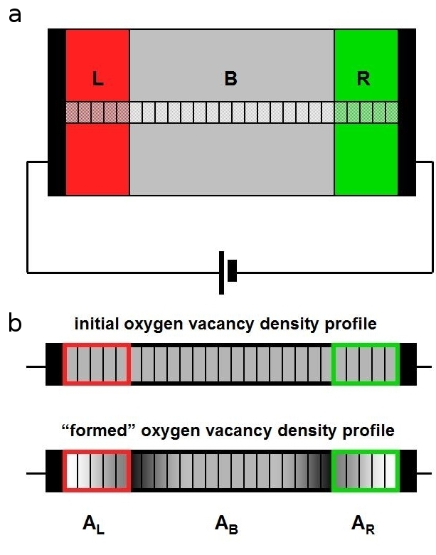
Our model is schematically shown in Fig. 1 and consists of a single conductive channel within a more insulating dielectric, which is represented by a one dimensional resistive network on links. The first and last links correspond to high resistance interfacial regions next to the external electrode, and the central links describe the bulk section. Each link is characterized by a certain concentration of oxygen vacancies, which determines the resistivity of the link. They may be physically associated to small domains of nanoscopic dimensions which may actually correspond to grains of the polycrystalline oxide. We take , with if is in the bulk (), if is in the left interface () and if is in the right interface (). In our study we set and . The following equation specifies how the vacancies diffuse through the network domains under an external voltage,
| (1) |
It gives the probability for transfer of vacancies from domain to a nearest neighbor domain . The probability is proportional to the concentration of vacancies present in domain and to the concentration of “available vacancy sites” at the target domain. The Arrhenius factor , is controlled by a dimensionless constant, , related to the activation energy for vacancies diffusion. The important factor models the enhancement (or suppression) of the diffusive process due to the local electric field at domain .
From Eq.(1), a constant leads to an initially constant distribution for all . The value of the initial constant concentration, must be much smaller than one, since it physically represents the concentration of defects (oxygen vacancies) within a domain. We adopt .
Similarly to actual resistive switching experiments, we simulate the applied voltage protocol by linear ramps that follow the sequence (our convention is that the right electrode is grounded). The duration is of time steps. The sequence may be repeated a number of cycles , for a total duration . In our simulations we choose , that provides a non-negligible but slow diffusive contribution to the evolution of with respect to the total time duration of the simulations (ie, the total number of time steps). We set that provides for a sufficiently large electric stress. Our qualitative results are rather robust with respect to the choice of model parameters, a detailed systematic study of their dependence is left for future work.
The coefficients , and still remain to be specified. With no loss of generality, we fix the value of the bulk coefficient to unity and leave the interfacial and free. In this initial study we shall concentrate in the symmetric case, , that corresponds to most common experimental devices.
The numerical simulations are performed through the following steps: (i) at each simulation time step () a given external voltage is applied to the resistive network (the electrodes are assumed perfect conductors). The current through the system is computed as , with the total (ie, two terminal) resistance
| (2) |
where denotes the three network regions, and denotes an unessential geometrical constant related to the dimensions of the domains (which we set to unity). (ii) we compute the local voltage profile and the voltages drops . (iii) we use Eq. (1) to compute all the oxygen vacancy transfers between nearest neighboring domains, and update the values to a new set of concentrations . (iv) we use these new values to recompute the current at under the applied voltage as indicated in the first step.
III Numerical Results and Comparison to Experiments
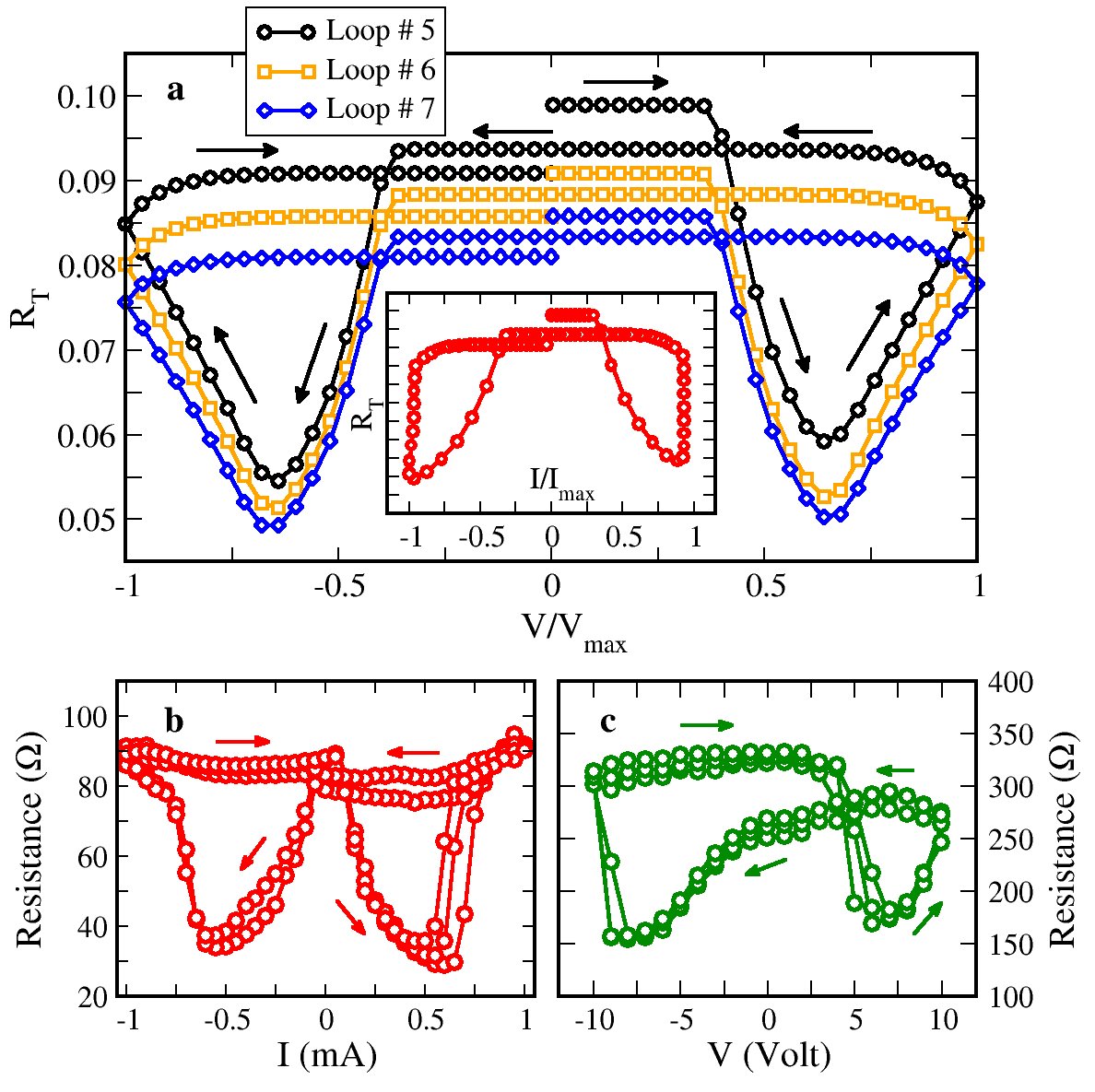
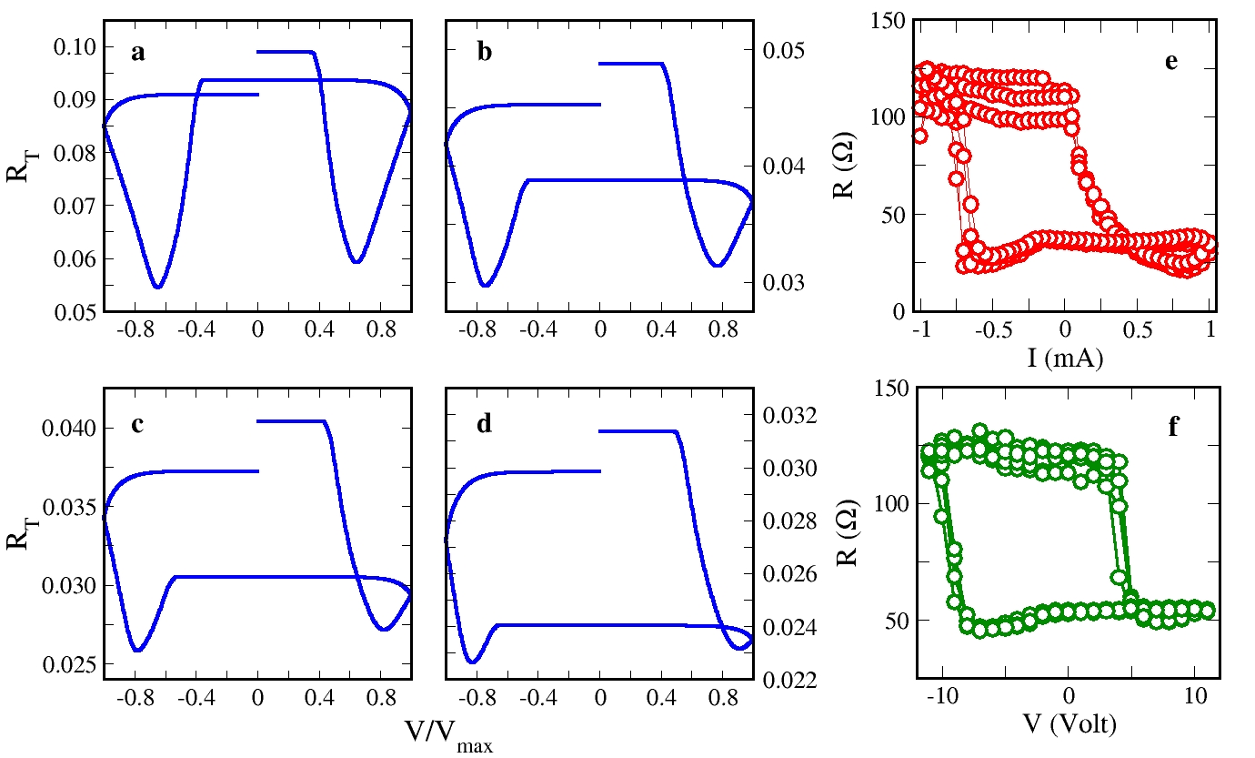
We now turn to the discussion of our results. We set , which is consistent with our experimental data and with previous reports in bulk and thin films of conducting perovskites nian ; quintero ; acha . In Fig. 2 we show the results for the hysteresis loop of the total resistance . The different data curves in Fig. 2a display the results in subsequent voltage cycles 5, 6, and 7. The inset of Fig. 2a, show that the hysteresis as a function of current remains qualitatively similar. We note that during the first few initial cycles the resistance shows non-repetitive memory effects that converge to a hysteresis loop with a stable shape. Interestingly, this is reminiscent of the initial “forming” that experimental samples seem to require in order to start displaying reproducible switching effects. The peculiar type of hysteresis loop that we obtain has been already reported by the Houston group ignatiev in experiments on (Pr,Ca)MnO3 manganite systems, where it has been termed “table with legs”. It is evidently a non-trivial effect and we have experimentally reproduced it in both, a related manganite (Pr,La,Ca)MnO3 and a cuprate (YBa2Cu3O7-x) sample, as shown in the bottom panels of Fig. 2.
There are several features worth pointing out: During each voltage protocol loop, there is a clear variation of the resistance between a rather broad maximum for a large range of (ie, the “table”), and two relatively narrow minima (ie, the “legs”). These maximum and minima correspond to the high and low resistance states, and . The loops are approximately symmetric in which reflects the left-right symmetry of the system. Throughout the voltage loop, the system begins in the initial state and undergoes the sequence of resistance changes under positive bias, and then under negative bias. The final state, at zero bias is , very close but not identical to the previous initial state. Interestingly, a similar small drift is also observed in the experimental data.
The qualitative agreement between our prediction of the “table with legs” and the experimentally observed hysteresis loops provides a significant validation for our model. Therefore, to gain physical insight into the mechanism of the RS effect we shall discuss in detail the evolution of the vacancies distribution under the applied voltage protocol.
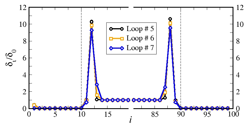
In Fig. 3 we show successive snapshots of the oxygen vacancy concentration profile at the beginning of loops 5, 6 and 7. Recalling that the initial equilibrium distribution of oxygen vacancy concentration is uniform , these curves reveal that, under the action of the repetitive voltage cycling, the evolve towards a new stable distribution. The salient features of the profile are a significant depletion in the interfacial regions and a strong accumulation peaks at both internal boundaries between the bulk and the interfacial regions. The reason can be understood as follows. The largest electric fields occur at the two interfacial regions since initially their resistance is much larger than the bulk one (, ). Therefore, oxygen vacancy migration is enhanced in the interfacial regions, with the ions moving either towards the electrodes or the bulk, depending on the direction of the applied voltage. When the ions reach the metallic electrodes they start to pile-up nian . On the other hand, the vacancies that migrate towards the bulk eventually leave the interfacial region and enter the bulk. There, their diffusion virtually stops, since the electric fields in the more conducting bulk are much smaller. Successive initial cycles yield a cumulative effect, with a depletion of the interfacial regions (and some pile-up at the edges) and a concomitant accumulation at the bulk side of the interfacial/bulk boundary. Significantly this accumulation, as seen in Fig. 3, is quite large and narrow leading to a substantial increase in the local resistance. This feature will be a key to understand the origin of the legs of the hysteresis loop, which we shall consider next.
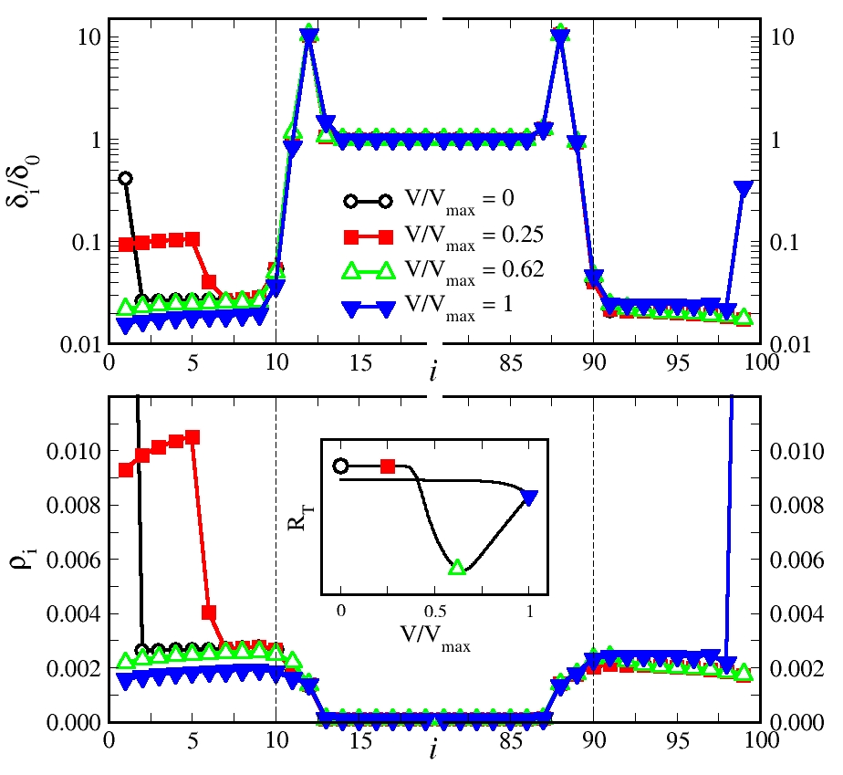
In Fig. 4 we show snapshots, during the first half of the voltage cycle, of the vacancy concentration and local resistance profiles in the interfacial regions and their boundaries with the bulk. These are the active regions of the system where the electric-field-enhanced migration takes place. Notice that since the current is uniform along the conductive path, the local electric fields are directly proportional to the local resistance. Let’s start at =0, from the state at the beginning of a cycle. Interestingly, the profile indicates significant electric fields in both interfacial regions which extends into the neighboring bulk. Thus the depletion of vacancies in the interfaces and the accumulation at the boundaries are such that compensate for the difference between the respective coefficients, to yield similar electric fields across the boundaries of the regions. Yet, at the very left end of the system there is a small pile-up of vacancies which, as soon as the voltage is ramped up, will translate into the largest local fields and initiate the ionic migration. At =0.25, we observe a snapshot of the migration of the vacancies across the left interfacial region towards the bulk. From the resistance expression Eq. (2), so long the vacancies remain within the interfacial region, the system remains in state. At =0.62, the vacancies have moved out the left interfacial region and entered the bulk, where their migration suddenly stops. Once in the bulk, the contribution to the total resistance of these migrating vacancies is reduced (), thus the system reaches the state (leg of the table). Notice that in this state, the largest fields occur at the boundaries of the bulk and the interfacial regions. Thus, as is further increased, the left interfacial region depletes further and therefore the voltage drop gets lower there. In contrast, on the right side the electric fields are further enhanced and there is now a migration of vacancies from the accumulation peak of the bulk towards the right interfacial region. This leads to an increase of the total resistance and, at the maximal voltage =1, we find that the vacancies have entered the interfacial region and already piled-up at the right end. Thus, the system is back to . The voltage protocol continues with the decrease of back to zero but keeping the same (positive) polarity. Therefore no significant change in the and profiles occurs, and half of the table with legs is already formed. When the negative polarity part of the cycle begins a similar analysis follows, since the distribution of vacancy concentrations is a mirror image of the initial one. This forms the other half of the table.
To complete our study we consider the effect of introducing an asymmetry in the model parameters and . In Fig. 5 we display the results for the hysteresis loops upon increasing the asymmetry. The results of the simulations show the gradual evolution of the “table with legs” towards a conventional rectangular hysteresis cycle ignatiev . Asymmetry in experimental samples can either be due to the fabrication process, as for instance, in the obvious case of using different type of metal for the electrodes. Though our samples were fabricated in a symmetric configuration, we induced a significant asymmetry by vigorous pulsing with a given polarity (ie, poling) before measuring the resistance hysteresis characteristic. Significantly, as shown in Fig. 5, we find that the experimental data obtained in an asymmetric manganite sample and the cuprate, induced by intensive same polarity pulsing, are in good qualitative agreement with our simulations. These results provides additional validation to our model.
IV Conclusions
To conclude, our results put on solid theoretical grounds the key role played by oxygen vacancies in the mechanism of resistive switching in TMO. They also provide valuable insights, predicting a non-trivial spatial profile of the oxygen vacancy distribution which may be of help for device design. An exciting idea for future work is to explore the possibility of using atomistic, first principles, calculations to study properties of electrode - transition metal oxide interfaces to estimate the parameters of the model and provide guidance in the material choice for actual memory devices.
ACKNOWLEDGMENTS
Support from CONICET (grants PIP 5254/05 and PIP 112-200801-00047) and ANCTyP (grants PICT 483/06 and PICT 837/07) is gratefully acknowledged.
References
- (1) G.I. Meijer, Science 319, 1625 (2008).
- (2) R. Waser and M. Aono, Nature Materials 6, 833 (2007).
- (3) A. Sawa, Materials Today 11, 28 (2008).
- (4) M. Janousch, G.I. Meijer, U. Staub, B. Delley, S.F. Karg, and B. P. Andreasson, Adv. Mat. 19, 2232 (2007).
- (5) K. Szot, W. Speier, G. Bihlmayer, and R. Waser, Nature Materials 5, 312 (2006).
- (6) I.H. Inoue, S. Yasuda, H. Akinaga, and H. Takagi, Phys. Rev. B 77, 035105 (2008).
- (7) K. Fujiwara, T. Nemoto, M.J. Rozenberg, Y., and H. Takagi, Jpn. J. App.Phys 47, 6266 (2008).
- (8) I.G. Baek, M.S. Lee, S. Seo, M.J. Lee, D.H. Seo, D.-S. Suh, J.C. Park, S.O. Park, H.S. Kim, I.K. Yoo, U.-In Chung, and J.T. Moon, Tech. Dig. IEDM. 587 (2004).
- (9) S.Q. Liu, N.J. Wu, and A. Ignatiev, Appl. Phys. Lett. 76 2749 (2000).
- (10) A. Beck, J.G. Bednorz, Ch. Gerber, C. Rossel, and D. Widmer, App. Phys. Lett. 77, 139 (2000).
- (11) Y. Watanabe, J.G. Bednorz, A. Bietsch, Ch. Gerber, D. Widmer, A. Beck, and S.J. Wind, App. Phys. Lett. 78, 3738 (2001).
- (12) B.J. Choi, D.S. Jeong, S.K. Kim, C. Rohde, S. Choi, J.H. Oh, H.J. Kim, C.S. Hwanga, K. Szot, R. Waser, B. Reichenberg, and S. Tiedke, J. Appl. Phys. 98, 033715 (2005).
- (13) A. Baikalov, Y.Q. Wang, B. Shen, B. Lorenz, S. Tsui, Y.Y. Sun, Y.Y. Xue, and C.W. Chu, Appl. Phys. Lett. 83 957 (2003).
- (14) Y.B. Nian, J. Strozier, N.J. Wu, X. Chen, and A. Ignatiev, Phys. Rev. Lett. 98, 146403 (2007).
- (15) N.A. Tulina, S.A. Zver’kov, Y.M. Mukovskii and D.A. Shulyatev, Europhys. Lett. 56, 836 (2001). N.A. Tulina, Physics-Uspekhi 50, 1171 (2007).
- (16) M.J. Rozenberg, I.H. Inoue and M.J. Sánchez, Phys. Rev. Lett. 92, 178302 (2004).
- (17) D.S. Jeong, H. Schroeder and R. Waser, Phys. Rev. B. 79, 195317 (2009).
- (18) D.-J. Seong, M. Jo, D. Lee, and H. Hwang, Electrochem. Solid-State Lett. 10 H168 (2007).
- (19) S. Tsui, A. Baikalov, J. Cmaidalka, Y.Y. Sun, Y.Q. Wang, Y.Y. Xue, C.W. Chu, L. Chen, and A.J. Jacobson, Appl. Phys. Lett. 85 317 (2004).
- (20) X. Chen, N.J. Wu, J. Strozier, and A. Ignatiev, Appl. Phys. Lett. 87 233506 (2005).
- (21) M. Quintero, P. Levy, A.G. Leyva and M.J. Rozenberg, Phys. Rev. Lett. 98 116601 (2007).
- (22) A. Sawa, T. Fujii, M. Kawasaki, and Y. Tokura, Appl. Phys. Lett. 85 4073 (2004).
- (23) T. Fujii, M. Kawasaki, A. Sawa, H. Akoh, Y. Kawazoe, and Y. Tokura, Appl. Phys. Lett. 86 012107 (2005).
- (24) A. Ignatiev, N.J. Wu, X. Chen, Y.B. Nian, C. Papagianni, S.Q. Liu, and J. Strozier, Phase Transitions 81, 791, (2008).
- (25) C. Acha and M. J. Rozenberg, J. Phys.: Condens. Matter 21, 045702, (2009).