Electron transport through a quantum
interferometer: A theoretical study
Santanu K. Maiti†,‡,111Corresponding Author: Santanu K. Maiti
Electronic mail: santanu.maiti@saha.ac.in
†Theoretical Condensed Matter Physics Division,
Saha Institute of Nuclear Physics,
1/AF, Bidhannagar, Kolkata-700 064, India
‡Department of Physics, Narasinha Dutt College,
129 Belilious Road, Howrah-711 101, India
Abstract
In the present work we explore electron transport properties through a quantum interferometer attached symmetrically to two one-dimensional semi-infinite metallic electrodes, namely, source and drain. The interferometer is made up of two sub-rings where individual sub-rings are penetrated by Aharonov-Bohm fluxes and , respectively. We adopt a simple tight-binding framework to describe the model and all the calculations are done based on the single particle Green’s function formalism. Our exact numerical calculations describe two-terminal conductance and current as functions of interferometer-to-electrode coupling strength, magnetic fluxes threaded by left and right sub-rings of the interferometer and the difference of these two fluxes. Our theoretical results provide several interesting features of electron transport across the interferometer, and these aspects may be utilized to study electron transport in Aharonov-Bohm geometries.
PACS No.: 73.23.-b; 73.63.Rt.
Keywords: Quantum interferometer; Conductance; - characteristic; AB effect; Anti-resonant states.
1 Introduction
The study of electronic transport in quantum confined model systems like quantum rings, quantum dots, arrays of quantum dots, quantum dots embedded in a quantum ring, etc., has become one of the most fascinating branch of nanoscience and technology. With the aid of present nanotechnological progress [1, 2], these simple looking quantum confined systems can be used to design nanodevices especially in electronic as well as spintronic engineering. The key idea of manufacturing nanodevices is based on the concept of quantum interference effect [3, 4, 5], and it is generally preserved throughout the sample having dimension smaller or comparable to the phase coherence length. Therefore, ring type conductors or two path devices are ideal candidates to exploit the effect of quantum interference [6]. In a ring shaped geometry, quantum interference effect can be controlled by several ways, and most probably, the effect can be regulated significantly by tuning the magnetic flux, the so-called Aharonov-Bohm (AB) flux [7, 8, 9, 10], that threads the ring. This key feature motivates us to widely use quantum interference devices in mesoscopic solid-state electronic circuits [11]. Using a mesoscopic ring we can construct a quantum interferometer, and here we will show that the interferometer exhibits several exotic features of electron transport which can be utilized in designing nanoelectronic circuits. To reveal the phenomena, we make a bridge system, by inserting the interferometer between two electrodes (source and drain), the so-called source-interferometer-drain bridge. Following the pioneering work of Aviram and Ratner [12], theoretical description of electron transport in a bridge system has got much progress. Later, many excellent experiments [13, 14, 15, 16, 17, 18, 19] have been done in several bridge systems to understand the basic mechanisms underlying the electron transport. Though extensive studies on electron transport have already been done both theoretically [7, 8, 9, 10, 20, 21, 22, 23, 24, 25, 26, 27, 28, 29, 30, 31, 32, 33, 34, 35, 36, 37, 38, 39, 40, 41, 42] as well as experimentally [13, 14, 15, 16, 17, 18, 19], yet lot of controversies are still present between the theory and experiment, and the complete description of the conduction mechanism in this scale is not very well defined even today. Several controlling factors are there which can significantly regulate electron transport in a conducting bridge, and all these factors have to be taken into account properly to understand the transport mechanism. For our illustrative purposes, here we mention some of these issues.
- 1.
-
2.
The coupling of the bridging material to the electrodes significantly controls the current amplitude across any bridge system [32].
-
3.
Dynamical fluctuation in small-scale devices is another important factor which plays an active role and can be manifested through the measurement of shot noise [36], a direct consequence of the quantization of charge.
-
4.
Geometry of the conducting material between the two electrodes itself is an important issue to control electron transmission which has been described quite elaborately by Ernzerhof et al. [42] through some model calculations.
Addition to these, several other factors of the tight-binding Hamiltonian that describe a system also provide important effects in the determination of current across a bridge system.
In this presentation we explore electron transport properties of a quantum interferometer based on the single particle Green’s function formalism. The interferometer is sandwiched between two semi-infinite one-dimensional (D) metallic electrodes, viz, source and drain, and, two sub-rings of the interferometer are subject to the Aharonov-Bohm (AB) fluxes and , respectively. The schematic view of the bridge system is depicted in Fig. 1. A simple tight-binding model is used to describe the system and all the calculations are done numerically, which illustrate conductance-energy and current-voltage characteristics as functions of the interferometer-to-electrode coupling strength, magnetic fluxes and the difference of these two fluxes. Several exotic features are observed from this study. These are: (i) semiconducting or metallic nature depending on the coupling strength of the interferometer to the side attached electrodes, (ii) appearance of anti-resonant states [7, 8, 9] and (iii) unconventional periodic behavior of typical conductance/current as a function of the difference of two AB fluxes.
The scheme of the paper is as follows. Following the introduction (Section ), in Section , we describe the model and theoretical formulation for the calculation. Section explores the results, and finally, we conclude our study in Section .
2 Model and synopsis of the theoretical background
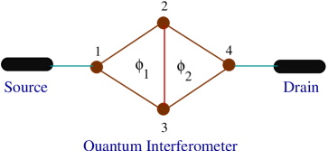
Let us begin with the model presented in Fig. 1. A quantum interferometer with four atomic sites (, where gives the total number of atomic sites in the interferometer) is attached symmetrically to two semi-infinite one-dimensional (D) metallic electrodes, namely, source and drain. The atomic sites and of the interferometer are directly coupled to each other, and accordingly, two sub-rings, left and right, are formed. These two sub-rings are subject to the AB fluxes and , respectively.
Considering linear transport regime, conductance of the interferometer can be obtained using the Landauer conductance formula [43, 44, 45, 46, 47],
| (1) |
where, becomes the transmission probability of an electron across the interferometer. It can be expressed in terms of the Green’s function of the interferometer and its coupling to the side-attached electrodes by the relation [46, 47],
| (2) |
where, and are respectively the retarded and advanced Green’s functions of the interferometer including the effects of the electrodes. Here and describe the coupling of the
interferometer to the source and drain, respectively. For the complete system i.e., the interferometer, source and drain, Green’s function is defined as,
| (3) |
where, is the injecting energy of the source electron. To Evaluate this Green’s function, inversion of an infinite matrix is needed since the complete system consists of the finite size interferometer and two semi-infinite electrodes. However, the entire system can be partitioned into sub-matrices corresponding to the individual sub-systems and the Green’s function for the interferometer can be effectively written as,
| (4) |
where, is the Hamiltonian of the interferometer that can be expressed within the non-interacting picture like,
| (5) |
In this Hamiltonian gives the on-site energy for the atomic site , where runs from to , () is the creation (annihilation) operator of an electron at the site and is the hopping integral between the nearest-neighbor sites and . For the sake of simplicity, we assume that the magnitudes of all hopping integrals () are identical to . The phase factor , associated with the hopping integral , comes due to the fluxes and in the two sub-rings. The phase factors () are chosen as, , , where , and is the elementary flux-quantum. Accordingly, a minus sign is used for the phases when the electron hops in the reverse direction. For the two D electrodes, a similar kind of tight-binding Hamiltonian is also used, except any phase factor, where the Hamiltonian is parametrized by constant on-site potential and nearest-neighbor hopping integral . The hopping integral between the source and interferometer is , while it is between the interferometer and drain. The parameters and in Eq. (4) represent the self-energies due to the coupling of the interferometer to the source and drain, respectively, where all the information of this coupling are included into these self-energies [46].
The current passing through the interferometer is depicted as a single-electron scattering process between the two reservoirs of charge carriers. The current can be computed as a function of the applied bias voltage by the expression [46],
| (6) |
where is the equilibrium Fermi energy. Here we assume that the entire voltage is dropped across the interferometer-electrode interfaces, and it is examined that under such an assumption the - characteristics do not change their qualitative features.
All the results in this communication are determined at absolute zero temperature, but they should valid even for some finite (low) temperatures, since the broadening of the energy levels of the interferometer due to its coupling to the electrodes becomes much larger than that of the thermal broadening [46]. On the other hand, at high temperature limit, all these phenomena completely disappear. This is due to the fact that the phase coherence length decreases significantly with the rise of temperature where the contribution comes mainly from the scattering on phonons, and accordingly, the quantum interference effect vanishes. Our unit system is simplified by choosing .
3 Numerical results and discussion
Before going into the discussion, let us first assign the values of different parameters those are used for our numerical calculation. The on-site energy of the interferometer is taken as for all the four sites , and the nearest-neighbor hopping strength is set to . On the other hand, for two side attached D electrodes the on-site energy () and nearest-neighbor hopping strength () are fixed to and , respectively. The equilibrium Fermi energy is set to .
Throughout the analysis we present the basic features of electron transport for two distinct regimes of electrode-to-interferometer coupling.
Case 1: Weak-coupling limit This limit is set by the criterion . In this case, we choose the values as .
Case 2: Strong-coupling limit This limit is described by the condition . In this regime we choose the values of hopping strengths as .
3.1 Interferometric geometry with atomic () sites
3.1.1 Conductance-energy characteristics
In Fig. 2, we plot conductance as a function of the injecting electron energy for the interferometer considering , where (a), (b), (c) and (d) correspond to , ,
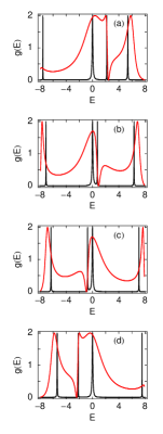
and , respectively. The black curves represent the results for the weak-coupling limit, while the results for the strong-coupling limit are shown by the red curves. In the limit of weak-coupling, conductance shows fine resonant peaks for some particular energies, while it () drops to zero almost for all other energies. At these resonances, conductance reaches the value , and therefore, the transmission probability becomes unity, since the relation is satisfied from the Landauer conductance formula (see Eq. (1) with ). The transmission probability of getting an electron across the interferometer significantly depends on the quantum interference of electronic waves passing through the different arms of the interferometer, and accordingly, the probability amplitude becomes strengthened or weakened. Now all the resonant peaks in the conductance spectra are associated with the energy eigenvalues of the interferometer, and thus it is emphasized that the conductance spectrum reveals itself the electronic structure of the interferometer. The situation becomes quite interesting as long as the coupling strength of the interferometer to the electrodes is increased from the weak regime to the strong one. In the strong-coupling limit, all the resonances get substantial widths compared to the weak-coupling limit. The contribution for the broadening of the resonant peaks in this strong-coupling limit appears from the imaginary parts of the self-energies and , respectively [46]. Hence, by tuning the coupling strength from the weak to strong regime, electronic transmission across the interferometer can be obtained for the wider range of energies, while a fine scan in the energy scale is needed to get the electron conduction across the bridge in the limit of weak-coupling. These results provide an important signature in the study of current-voltage (-) characteristics. Another interesting feature observed from the conductance spectra is the existence of the anti-resonant states. The positions of the anti-resonance states can be clearly noticed from the red curves, compared to the black curves since the widths of these curves are too small, where they sharply drop to zero for the respective energy values associated with the different values of (see Figs. 2(a)-(d)). Such anti-resonant states are specific to the interferometric nature of the scattering and do not occur in conventional one-dimensional scattering problems of potential barriers [7, 8, 9]. A clear investigation shows that the positions of the anti-resonances on the energy scale are independent of the interferometer-to-electrode coupling strength. Since the width of these anti-resonance states are too small, they do not provide any significant contribution in the current-voltage (-) characteristics.
3.1.2 Typical conductance as a function of
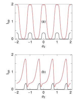
The effect of , the difference between two AB fluxes
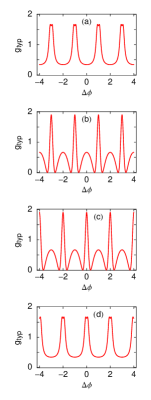
and , on the electron transport through the interferometer is also an important issue in the present context. To visualize it, in Fig. 3, we display the variation of the typical conductance () as a function of for the interferometer in the limit of strong-coupling. Figures 3(a), (b), (c) and (d) correspond to the results for , , and , respectively. The typical conductances are calculated for the fixed energy . Very interestingly we observe that, for a fixed value of , typical conductance varies periodically with showing (, since in our chosen unit) flux-quantum periodicity, associated with the number of atomic sites () in the vertical line connecting two sub-rings of the quantum interferometer. This period doubling behavior is completely different from the traditional periodic nature, since in conventional geometries we get simple flux-quantum periodicity. In the limit of weak-coupling we will also get the similar behavior of periodicity () for the typical conductance with , and due to the obvious reason we do not plot the results for this coupling limit once gain.
3.1.3 Current-voltage characteristics
All these features of electron transfer become much more clearly visible by studying the current-voltage (-) characteristics. The current passing through the interferometer is computed from the integration procedure of the transmission function as prescribed in Eq. (6) which is not restricted in the linear response regime, but it is of great significance in determining the shape of the full current-voltage characteristics. As illustrative examples, in Fig. 4, we plot the current-voltage characteristics of the interferometer for the three different values of , keeping the flux in the left sub-ring to a fixed value . The red, blue and black curves correspond to , and , respectively. In the limit of weak-coupling (see Fig. 4(a)), it is observed that the current exhibits staircase-like structure with fine steps as a function of the applied bias voltage . This is due to the existence of the sharp resonant peaks in the conductance spectrum in this coupling limit, since the current is computed by the integration method of the transmission function . With the increase of the bias voltage , the electrochemical potentials on the electrodes are shifted gradually, and finally cross one of the quantized energy levels of the interferometer. Accordingly, a current channel is opened up which provides a jump in the
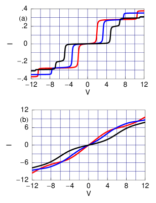
- characteristic curve. The most important feature observed from the - curves for this weak-coupling limit is that, the non-zero value of the current appears beyond a finite bias voltage, the so-called threshold voltage . This is quite analogous to the semiconducting nature of a material. Most interestingly, the results predict that the threshold bias voltage of electron conduction can be controlled very nicely by tuning the AB flux . The situation becomes much different for the strong-coupling case. The results are given in Fig. 4(b). In this limit, the current varies almost continuously with the applied bias voltage and achieves much larger amplitude than the weak-coupling case. The reason is that, in the limit of strong-coupling all the energy levels get broadened which provide larger current in the integration procedure of the transmission function . Thus by tuning the strength of the interferometer-to-electrode coupling, we can achieve very large, even an order of magnitude, current amplitude from the very low one for the same bias voltage , which provides an important signature in designing nanoelectronic devices. In contrary to the weak-coupling limit, here the electron starts to conduct as long as the bias voltage is given i.e., , which reveals the metallic nature. Thus it can be emphasized that the interferometer-to-electrode coupling is a key parameter which controls the electron transport in a meaningful way. Additionally, the existence of the semiconducting or the metallic behavior of the interferometer also significantly depends on the AB fluxes and . The nature of all these - curves, presented in Fig. 4, will be exactly similar if we plot the results for the different values of , keeping as a constant.
3.1.4 Typical current amplitude as a function of
Now, we draw our attention on the variation of the typical current amplitude with anyone of these two fluxes, when the other one is fixed. To explore it, in Fig. 5, we show the variation of the typical current amplitude () with , considering as a constant, where (a) and (b) correspond to and , respectively. The black and red lines represent the results for the weak- and strong-coupling limits, respectively. The typical current amplitudes are calculated for the fixed bias voltage . Both for these two limiting cases, the typical current amplitude varies periodically with , exhibiting flux-quantum periodicity, as expected. Similar feature is also observed for the vs curves, when becomes constant. Here it is also important to note that the variation of with is quite similar to that as presented in Fig. 3. The typical current amplitude varies periodically with
showing flux-quantum periodicity, following the - characteristics.
With the above description of electron transport for a -site () quantum interferometer, now we can extend our discussion for an interferometer with higher number of atomic sites i.e., .
3.2 Interferometric geometry with atomic () sites
To get an experimentally realizable system, here we consider a quantum interferometer with large number of atomic sites compared to our presented mathematical model with atomic sites. The schematic view of such a quantum interferometer is given in Fig. 6, where we set . The vertical line connecting left and right sub-rings contains
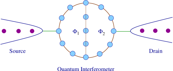
atomic sites, where the individual sub-rings are penetrated by AB fluxes and , respectively. In this interferometric geometry, the phase factors (’s) are chosen according
to our earlier prescription. Along the circumference of the ring and along the vertical line , where and correspond to the identical meaning as before.
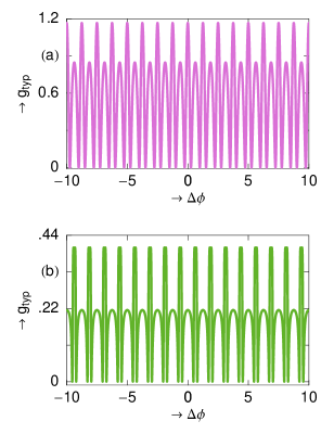
For this bigger quantum interferometer (), exactly similar features of conductance-energy and current-voltage characteristics are observed as we see in the case of a -site interferometer. Also, typical current amplitude shows identical variation with to our previous study. Only the typical conductance varies in a different way as a function of . As illustrative examples in Fig. 7 we plot - characteristics for the quantum interferometer with in the limit of strong-coupling, where (a) and (b) correspond to and , respectively. The typical conductances are determined at the energy . From the spectra we notice that for a fixed value of , typical conductance oscillates as a function of exhibiting flux-quantum periodicity. This phenomenon is completely different from the traditional periodic nature. Comparing the results presented in Figs. 3 and 7 it is manifested that the periodicity of - curves depends on the total number of atomic sites in the vertical line connecting left and right sub-rings of a quantum interferometer. Therefore, changing the length of the vertical line, periodicity can be changed accordingly.
4 Closing remarks
To summarize, we have explored electron transport properties through a quantum interferometer using the single particle Green’s function formalism. We have adopted a simple tight-binding framework to illustrate the bridge system, where the interferometer is sandwiched between two electrodes, viz, source and drain. We have done exact numerical calculation to study conductance-energy and current-voltage characteristics as functions of the interferometer-to-electrode coupling strength, magnetic fluxes and penetrated by left and right sub-rings of the interferometer and the difference of these two fluxes. Several key features of electron transport have been observed those may be useful in manufacturing nanoelectronic devices. The most exotic features are: (i) existence of semiconducting or metallic behavior, depending on the interferometer-to-electrode coupling strength, (ii) appearance of the anti-resonant states and (iii) unconventional periodic behavior of the typical conductance/current as a function of the difference of two AB fluxes.
Throughout our work, we have addressed the essential features of electron transport through a quantum interferometer with total number of atomic sites . Next, we have extended our discussion for an interferometer with higher number of atomic sites where we set to achieve an experimentally realizable system. In our model calculations, these typical numbers ( and ) are chosen only for the sake of simplicity. Though the results presented here change numerically with ring size (), but all the basic features remain exactly invariant. To be more specific, it is important to note that, in real situation experimentally achievable rings have typical diameters within the range - m. In such a small ring, very high magnetic fields are required to produce a quantum flux. To overcome this situation, Hod et al. have studied extensively and proposed how to construct nanometer scale devices, based on Aharonov-Bohm interferometry, those can be operated in moderate magnetic fields [48, 49, 50, 51, 52].
This is our first step to describe the electron transport in a quantum interferometer. Here we have made several realistic approximations by ignoring the effects of electron-electron correlation, electron-phonon interaction, disorder, temperature, etc. Over the last few many years people have studied a lot to incorporate the effect of electron-electron correlation in the study of electron transport, yet no such proper theory has been well established. Thus the inclusion of electron-electron correlation in the present model is a major challenge to us. The presence of electron-phonon interaction in Aharonov-Bohm interferometers provides phase shifts of the conducting electrons and due to this dephasing process electron transport through an AB interferometer becomes highly sensitive to the AB flux with the increase of electron-phonon coupling strength [53]. In the present work, we have addressed our results considering the site energies of all the atomic sites of the interferometer are identical i.e., we have treated the ordered system. But in real case, the presence of impurities will affect the electronic structure and hence the transport properties. The effect of the temperature has already been pointed out earlier, and, it has been examined that the presented results will not change significantly even at finite temperature, since the broadening of the energy levels of the interferometer due to its coupling to the electrodes will be much larger than that of the thermal broadening [46]. At the end, we would like to mention that we need further study in such systems by incorporating all these effects.
The importance of this article is mainly concerned with (i) the simplicity of the geometry and (ii) the smallness of the size, and our exact analysis may be utilized to study electron transport in Aharonov-Bohm geometries.
References
- [1] J. Chen, M. A. Reed, A. M. Rawlett, J. M. Tour, Science 286 (1999) 1550.
- [2] P. Ball, Nature (London) 404 (2000) 918.
- [3] Y. Imry, Introduction to Mesoscopic Physics, Oxford University Press, Oxford (2002).
- [4] Y. Imry, R. Landauer, Rev. Mod. Phys. 71 (1999) S306.
- [5] Y. Gefen, arXiv:cond-mat/0207440v1.
- [6] Y. Aharonov, D. Bohm, Phys. Rev. 115 (1959) 485.
- [7] K.-W. Chen, C.-R. Chang, J. Appl. Phys. 103 (2008) 07B708.
- [8] Y. Han, W. Gong, H. Wu, G. Wei, Physica B 404 (2009) 2001.
- [9] Z.-B. He, Y.-J. Xiong, Phys. Lett. A 349 (2006) 276.
- [10] S. Welack, S. Mukamel, Y. Yan, Eur. Phys. Lett. 85 (2009) 57008.
- [11] D. Rohrlich, O. Zarchin, M. Heiblum, D. Mahalu, V. Umansky, Phys. Rev. Lett. 98 (2007) 096803.
- [12] A. Aviram, M. Ratner, Chem. Phys. Lett. 29 (1974) 277.
- [13] A. W. Holleitner, R. H. Blick, A. K. Hüttel, K. Eberl, J. P. Kotthaus, Science 297 (2002) 70.
- [14] K. Kobayashi, H. Aikawa, S. Katsumoto, Y. Iye, Phys. Rev. Lett. 88 (2002) 256806.
- [15] K. Kobayashi, H. Aikawa, A. Sano, S. Katsumoto, Y. Iye, Phys. Rev. B 70 (2004) 035319.
- [16] Y. Ji, M. Heiblum, H. Shtrikman, Phys. Rev. Lett. 88 (2002) 076601.
- [17] A. Yacoby, M. Heiblum, D. Mahalu, H. Shtrikman, Phys. Rev. Lett. 74 (1995) 4047.
- [18] J. Chen, M. A. Reed, A. M. Rawlett, J. M. Tour, Science 286 (1999) 1550.
- [19] M. A. Reed, C. Zhou, C. J. Muller, T. P. Burgin, J. M. Tour, Science 278 (1997) 252.
- [20] P. A. Orellana, M. L. Ladron de Guevara, M. Pacheco, A. Latge, Phys. Rev. B 68 (2003) 195321.
- [21] P. A. Orellana, F. Dominguez-Adame, I. Gomez, M. L. Ladron de Guevara, Phys. Rev. B 67 (2003) 085321.
- [22] A. Nitzan, Annu. Rev. Phys. Chem. 52 (2001) 681.
- [23] A. Nitzan, M. A. Ratner, Science 300 (2003) 1384.
- [24] Z. Bai, M. Yang, Y. Chen, J. Phys.: Condens. Matter 16 (2004) 2053.
- [25] V. Mujica, M. Kemp, M. A. Ratner, J. Chem. Phys. 101 (1994) 6849.
- [26] V. Mujica, M. Kemp, A. E. Roitberg, M. A. Ratner, J. Chem. Phys. 104 (1996) 7296.
- [27] W. Y. Cui, S. Z. Wu, G. Jin, X. Zhao, Y. Q. Ma, Eur. Phys. J. B. 59 (2007) 47.
- [28] R. Baer, D. Neuhauser, J. Am. Chem. Soc. 124 (2002) 4200.
- [29] D. Walter, D. Neuhauser, R. Baer, Chem. Phys. 299 (2004) 139.
- [30] K. Tagami, L. Wang, M. Tsukada, Nano Lett. 4 (2004) 209.
- [31] K. Walczak, Cent. Eur. J. Chem. 2 (2004) 524.
- [32] R. Baer, D. Neuhauser, Chem. Phys. 281 (2002) 353.
- [33] S. K. Maiti, Physica E 40 (2008) 2730.
- [34] S. K. Maiti, Physica E 36 (2007) 199.
- [35] S. K. Maiti, J. Phys. Soc. Jpn. 78 (2009) 114602.
- [36] K. Walczak, Phys. Stat. Sol. (b) 241 (2004) 2555.
- [37] D. I. Golosov, Y. Gefen, Phys. Rev. B 74 (2006) 205316.
- [38] T. Kubo, Y. Tokura, T. Hatano, S. Tarucha, Phys. Rev. B 74 (2006) 205310.
- [39] T. Nakanishi, K. Terakura, T. Ando, Phys. Rev. B 69 (2004) 115307.
- [40] O. Entin-Wohlman, Y. Imry, A. Aharony, Phys. Rev. B 70 (2004) 075301.
- [41] B. Kubala, J. König, Phys. Rev. B 65 (2002) 245301.
- [42] M. Ernzerhof, M. Zhuang, P. Rocheleau, J. Chem. Phys. 123 (2005) 134704.
- [43] R. Landauer, Phys. Lett. A 85 (1986) 91.
- [44] R. Landauer, IBM J. Res. Dev. 32 (1988) 306.
- [45] M. Büttiker, IBM J. Res. Dev. 32 (1988) 317.
- [46] S. Datta, Electronic transport in mesoscopic systems, Cambridge University Press, Cambridge (1997).
- [47] M. B. Nardelli, Phys. Rev. B 60 (1999) 7828.
- [48] O. Hod, R. Baer, E. Rabani, J. Phys. Chem. B 108 (2004) 14807.
- [49] O. Hod, R. Baer, E. Rabani, J. Phys.: Condens. Matter 20 (2008) 383201.
- [50] O. Hod, R. Baer, E. Rabani, J. Am. Chem. Soc. 127 (2005) 1648.
- [51] O. Hod, E. Rabani, R. Baer, Acc. Chem. Res. 39 (2006) 109.
- [52] O. Hod, E. Rabani, R. Baer, J. Chem. Phys. 123 (2005) 051103.
- [53] O. Hod, R. Baer, E. Rabani, Phys. Rev. Lett. 97 (2006) 266803.