Solid-state memcapacitor
Abstract
We suggest a possible realization of a solid-state memory capacitive (memcapacitive) system. Our approach relies on the slow polarization rate of a medium between plates of a regular capacitor. To achieve this goal, we consider a multi-layer structure embedded in a capacitor. The multi-layer structure is formed by metallic layers separated by an insulator so that non-linear electronic transport (tunneling) between the layers can occur. The suggested memcapacitor shows hysteretic charge-voltage and capacitance-voltage curves, and both negative and diverging capacitance within certain ranges of the field. This proposal can be easily realized experimentally, and indicates the possibility of information storage in memcapacitive devices.
I Introduction
A recent experimental demonstration of a nanoscale memory-resistor (memristor for short) Strukov et al. (2008) has sparked numerous investigations in the area of materials and systems that show history-dependence in their current-voltage characteristics Pershin and Di Ventra (2008); Pershin et al. (2009); Driscoll et al. (2009a, b); Waser and Aono (2007); Scott and Bozano (2007). This has also led to the recent proposal and theoretical investigation of memcapacitors and meminductors, namely capacitors and inductors whose capacitance and inductance, respectively, depends on the past states through which the system has evolved Di Ventra et al. (2009a). Together with the memristor, the whole class of these memory-circuit elements promises new and unexplored functionalities in electronics, and the combination of these memory devices with their “standard” counterpart may find application in disparate areas of science and technology, including the study of neuromorphic circuits to simulate biological processes Di Ventra et al. (2009b). In this paper, we focus only on memcapacitors.
Various systems are known to exhibit memcapacitive behavior including vanadium dioxide metamaterials Driscoll et al. (2009a), nanoscale capacitors with interface traps or embedded nanocrystals Kim et al. (2001); Fleetwood et al. (1995); Su et al. (2005); Lee et al. (2006), and elastic capacitors Nieminen et al. (2002); Partensky (2002). As anticipated in Ref. Di Ventra et al., 2009a, memcapacitive effects may also accompany memristive effects in nanostructures, since in many of them the morphology of conducting regions changes in time Strukov et al. (2008). Moreover, memcapacitors can be simulated by electronic circuits Pershin and Di Ventra (2009). However, the number of experimentally identified memcapacitive systems is still very limited. In addition, it would be of great importance to identify a mamcapacitive system that can be fabricated relatively easily, and is flexible enough to cover a wide range of capacitances.
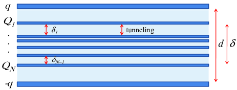
Here, we suggest a possible realization of such a system based on the slow polarization of a medium between a regular capacitor plates. There are several physical mechanisms that can potentially provide a slowly polarizable medium. Examples include tunneling, activated drift of charged vacancies/impurities, slow ion penetration through a membrane, etc. In this paper, we will consider the tunneling mechanism and discuss a solid-state memcapacitive system consisting of metal layers embedded into a parallel-plate capacitor as schematically shown in Fig. 1. In this realization, the internal metal layers, together with the insulator material, form a “metamaterial” characterized by a long polarization/depolarization time. The application of an external voltage to the capacitor leads to a charge redistribution between the embedded metal layers. The tunneling current between the layers depends almost exponentially on the applied voltage. This feature is important for the operation of our suggested device allowing for the “writing” of information (in the form of medium polarization) with high-voltage pulses, and “holding” such information when low/zero voltages are applied. The resulting memcapacitor exhibits not only hysteretic charge-voltage and capacitance-voltage curves but also both negative and diverging capacitance within certain ranges of the field. Due to its simplicity and unusual capacitance features we thus expect it to find use in both logic and memory applications.
This paper is organized as follows. Sec. II describes the theoretical framework used to simulate solid-state memcapacitors. Numerical simulations for the case of ac and pulsed applied voltages are presented in Sec. III and IV, respectively. An equivalent circuit model is given in Sec. V. Finally, Sec. VI presents our conclusions.
II Model
Quite generally, a circuit element with memory (memristor, memcapacitor or meminductor) is defined by the relations Di Ventra et al. (2009a)
| (1) | |||||
| (2) |
where and are any two input and output variables (i.e., current, charge, voltage, or flux), is a generalized response, is a set of state variables describing the internal state of the system, and is a continuous -dimensional vector function. In this paper we will be concerned with only memcapacitors. Therefore, using Eqs. (1, 2), we define a charge-controlled memcapacitive system by the equations
| (3) | |||||
| (4) |
where is the charge on the capacitor at time , is the applied voltage, and is the memcapacitance, which depends on the state of the system and can vary in time. Below, we identify the internal state variables of the solid-state memcapacitor shown in Fig. 1 and demonstrate that such memcapacitor is indeed described by Eqs. (3,4).
Let us then consider the system schematically shown in Fig. 1 consisting of layers of metallic regions separated by an insulating material. This multi-layer system, of thickness , is embedded into a standard parallel-plate capacitor. For convenience, although this is not necessary, we assume that the insulating material in between the embedded metallic layers is the same as the one of the regular capacitor. We also assume that our memcapacitor is designed in such a way that there is no electron exchange between the external plates and those embedded. This can be achieved by selecting an appropriate separation between the internal metal layers and the capacitor plates and/or by using an insulating material between the external capacitor plates and the embedded ones that generates a higher potential barrier. Therefore, in what follows, we assume that the tunneling only occurs between the internal metallic layers. Consequently, the total internal charge is always zero: , where is the charge on the internal metal layers at time .
The operation of the polarization-based memcapacitor relies on the redistribution of the internal charges between the embedded layers caused by the electric field due to the charge on the capacitor plates. Polarization of the metamaterial results in an internal electric field between the layers that is opposite to the electric field due to the plate charges. Therefore, for a given amount of plate charge, the internal charges tend to decrease the plate voltage or, equivalently, to increase the capacitance.
Let us then calculate the internal charge distribution and consequent capacitance. A charged plane creates a uniform electric field in the direction perpendicular to the plane with a magnitude , where is the surface (of area ) charge density, is the vacuum permittivity, and is the relative dielectric constant of the insulating material. Using this expression, we find that, in the structure shown in Fig. 1, the external plate voltage is given by,
| (5) | |||||
where is the electric field due to the charge at the external plate and is the electric field due to the charge at the -th embedded metal layer. Eq. (5) can also be written as follows
| (6) | |||||
where , for , , and is the capacitance of the system without internal metal layers. Therefore, the capacitance of the whole structure is
| (7) |
From this equation it is already clear that, unlike a conventional capacitor, there may be instants of time in which the denominator of Eq. (7) is zero while the numerator is finite. This may happen when the internal metal layers screen completely the external field, despite the presence of a finite charge on the external capacitor plates. At these times one would then expect diverging values of capacitance. In addition, Eq. (7) does not enforce a positive capacitance. Indeed, as we will show in the examples below, at certain instants of time the internal metal layers may over-screen the external field, resulting in a negative capacitance. It is interesting to note that an hysteretic negative and diverging capacitance has been found also in ionic memcapacitors, namely nanopore membranes in an ionic solution subject to external time-dependent perturbations Krems et al. (2009). A negative capacitance has been experimentally observed in different solid-state systems Ershov et al. (1998); Gommans et al. (2005); Mora-Sero et al. (2006), but not accompanied by hysteretic and diverging values of capacitance.
In order to describe the dynamics of the internal charges , let us define as the voltage between and metal layers. The electric field between two neighboring layers is obtained by adding the electric fields due to charges at all layers and at the external metal plates:
| (8) |
The dynamics of the charge at a metal layer is then determined by the currents flowing to and from that layer:
| (9) |
where is the tunneling electron current flowing from layer to layer (note that for the top and bottom layers (), there is only one term on the right hand side of Eq. (9)). By considering the layer charges as state variables, we immediately notice that Eq. (9) is similar to Eq. (4). This demonstrates that the system under consideration is indeed a charge-controlled memcapacitive system.
If is the potential barrier height between two adjacent metal layers (see inset of Fig. 2), the tunneling current induced by the voltage difference between the two can be calculated using the following expressions Simmons (1963)
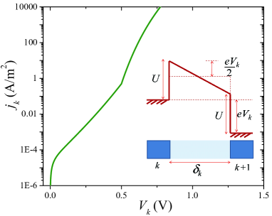
| (10) |
if , and
| (11) |
if . In the above equations, is the Planck constant. The tunneling current density as a function of voltage drop is depicted in Fig. 2 for two adjacent layers. A strong increase in current with increase of is clearly observed. This is an important property for the operation of our suggested memcapacitor.
III AC voltage operation
In this Section, we present results of numerical simulations obtained for the case of a sinusoidal voltage of amplitude and frequency applied to a memcapacitor connected in series with a resistor . Such a circuit is described by the equation
| (12) |
where, for , we use Eq. (7). Eq. (12) is solved numerically together with Eq. (9) describing the internal charge dynamics. Below, we present results of numerical simulations for two different memcapacitor structures. In our simulations, a small value of is selected so that the voltage drop on the resistor is negligible.
III.1 2-layer memcapacitor
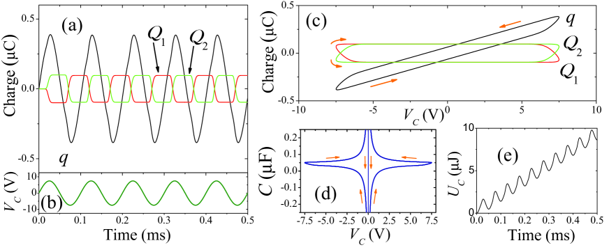
The simplest system exhibiting polarization memory is a two-layer memcapacitor. In Fig. 3 we illustrate simulation results of such a device. Starting at the zero-charge state, the sinusoidal applied voltage induces electron tunneling between the internal metal layers resulting in non-zero and . As it is shown in Fig. 3(a), positive half-periods of induce negative and positive charges. In turn, these cause a screening electric field opposite to the electric field of plate charges.
It is interesting that on the charge-voltage plot (Fig. 3(c)), forms a non-pinched hysteresis loop. This is a quite unusual feature of a memory device, especially, in view of the fact that, at the present time, only memristive devices exhibiting pinched hysteresis loops have been observed experimentally. Physically, it is clear that when an internal polarization in the memcapacitor is present and the plate charge is zero (), the internal polarization creates a non-zero voltage drop on the device . Alternatively, this voltage drop can be compensated by plate charges, but then we get at . This explains why the curve does not pass through the (0,0) point. The corresponding capacitance hysteresis is shown in Fig. 3(d). As expected, we find both negative and diverging capacitance values. In the vicinity of , the capacitance changes from to at both sweep directions. In Fig 3(d), these abrupt changes appear as two coinciding vertical lines.
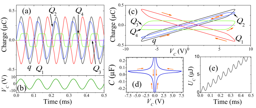
Next, we consider the added/removed energy to/from the capacitor which is defined as
| (13) |
From Fig. 3(e) it is clear that the present solid-state memcapacitor operates as a dissipative device since the amount of added energy is on average larger than the amount of removed energy (resulting in positive values of at all times). This occurs because the electron tunneling between internal layers is accompanied by energy dissipated in thermalization processes due to the different electrochemical potential energies of metal layers. In addition, in a real device we cannot exclude the phenomenon of local heating that would also contribute to dissipation of energy Di Ventra (2008).
In fact, the energy dissipation in electron transfer processes or the usual energy dissipation in dielectric materials described by the imaginary part of the complex permittivity can be used as an alternative to our approach. The heat released can drive a phase transition in a material between the plates, such as transition from crystalline to amorphous state and vice versa, accompanied by a change in material’s permittivity. In this way, the memcapacitor acquires a long-term memory based directly on the value of . The required material for this purpose can be similar to chalcogenide glass, which can be ”switched” between two states, crystalline or amorphous, with the application of heat, but possibly at a lower phase transition temperature. The device operation protocol can then be based in applications of ac-modulated voltage pulses whose amplitude, duration or frequency can control the material’s state.
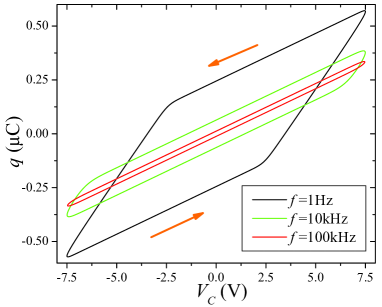
Finally, the frequency behavior of the charge-voltage hysteresis loop is shown in Fig. 4. It is clearly seen that the hysteresis shrinks at higher frequencies. This is a typical behavior of memory devices Di Ventra et al. (2009a) related to the fact that at high frequencies the internal degrees of freedom of a memory device do not have enough time to respond to the external perturbation. Similarly, with increasing frequency, we have observed a decrease in capacitance hysteresis as well as in the rate of energy dissipation.
III.2 Multi-layer memcapacitor
The results obtained for multi-layer memcapacitors are similar to the two-layer memcapacitor case. The only interesting difference is that in the case of multi-layer memcapacitors, a richer internal charge dynamics can be observed. Charge dynamics is essentially determined by the distance between the layers and the potential energy barrier between adjacent layers. As a prototype of multi-layer memcapacitor, we consider a four-layer memcapacitor.
In our particular example two additional internal layers (2-nd and 3-rd) were inserted between the two layers of the two-layer memcapacitor. The layers’ positions are specified in the caption of Fig. 5: layer 2 is positioned close to layer 1, while layer 3 is placed in between layers 2 and 4. As a result, the electron tunneling current can be high between 1-st and 2-nd layers which is reflected in high amplitudes of and . Concerning the charge on the third layer, it is essentially close to zero. We explain it by a tendency of maximum charge separation in these types of devices. Fig. 5 displays our simulation results for this case. One can also see that the capacitance hysteresis and the added/removed energy (Fig. 5 (d) and (e), respectively) are similar to those of the two-layer memcapacitor as shown in Fig. 3.
IV Retrieving the memcapacitor state
At this point, an important question is how one can read the memcapacitor state. Here, we demonstrate that the most simple way to do it is by using a single voltage pulse. Small amplitude or short voltage pulses are not suitable for this purpose as they do not change the charge distribution on the internal layers considerably. Therefore, the measured value of capacitance, using small amplitude or short pulses, would always be equal to , the capacitance in the absence of the internal metal layers. It is thus important to ensure that the applied pulse has a large enough amplitude and is sufficiently long. Consequently, the device state will be altered by the pulse. However, since the initial state is read by this measurement, this state can be, in principle, restored.
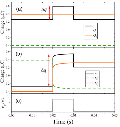
Fig. 6 illustrates the reading of the internal layer polarization in a two-layer memcapacitor. Quite generally, we start with a memcapacitor having a certain internal polarization and assume that at the initial moment of time the voltage drop on the memcapacitor is zero. Although this is not a steady state of the device (at and we expect ), the memcapacitor can stay in such a state sufficiently long since the tunneling current is exponentially suppressed at low internal fields. Our idea is to apply a single voltage pulse to the device and monitor the amount of charge needed to make close to the applied voltage . This amount of charge , as we show, depends on the device state.
In our particular calculations, we consider two cases characterized by a different initial polarization. When is negative at (Fig. 6(a)), the applied voltage pulse does not significantly change the device state (, ) and the amount of charge added to the plates is small (hence the capacitance is low). In the opposite case, when is positive at (Fig. 6(b)), much larger charge should be transferred to the capacitor plates since “re-programming” of the internal state is required. Therefore, this measurement would monitor a higher value of capacitance. We emphasize that the measured capacitance value is determined by both the system state and by the voltage probe. For the same system state but different probes (for example, pulses of different polarity but of same magnitude) the measured value of capacitance may be different.
V Equivalent circuit model
In this Section, we suggest an equivalent circuit model of the solid-state memcapacitor discussed above. This correspondence is very useful in circuit simulators, or in the realization of electronic circuits to reproduce memcapacitive features. The main idea behind the circuit model is to represent each insulator spacing between adjacent metal layers (including capacitor plates) by a separate capacitor and to use non-linear resistors in order to mimic the electron tunneling between the layers and energy loss in the thermalization processes accompanying the tunneling. The top and bottom surfaces of each internal layer are considered as plates of adjacent circuit model’s capacitors while the metallic material of the layer itself plays the role of the conductor connecting these capacitors.
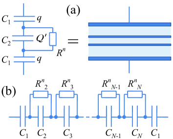
Fig. 7(a) shows the equivalent circuit of a two-layer memcapacitor. The circuit is composed by three capacitors connected in series. The capacitor in the middle is connected in parallel to a non-linear resistor (see Fig. 7(a)). The parameters of capacitors are determined by the usual parallel plate capacitor expression and related to the parameters of memcapacitor in the following way:
Next, we demonstrate the equivalence of the equations describing the circuit model and those of the memcapacitor. The circuit shown in Fig. 7(a) is described by the following two equations
| (14) | |||||
| (15) |
where the first equation is for the total voltage drop and the second equation is the Kirchhoff’s law for the currents. Here, stands for the current through the non-linear resistor which depends on the voltage drop on (equal to with the charge on capacitor ).
In order to relate Eqs. (16,17) to the memcapacitor equations from Sec. II, we note that the sum of charges at the bottom plate of (equal to ) and at the top plate of (equal to , see Fig. 7(a)) is equal to , that is the charge at the first layer of memcapacitor, i.e., . One then immediately notices that Eq. (16) and Eq. (7) (for the case of two layers) are exactly the same; Eq. (17) and Eq. (9) are also the same. This proofs the complete equivalence between memcapacitor’s and circuit model’s equations.
The extension of the circuit model to an -layer memcapacitor is straightforward: different capacitors and non-linear resistors must be introduced between the external capacitors . Fig. 7(b) shows the equivalent circuit model of an -layer memcapacitor. Another interesting model extension can be achieved if a memristive dielectric material (e.g., VO2 films Driscoll et al. (2009b)) is used instead of the usual dielectric in the device. Then, in the equivalent circuit model, the role of non-linear resistors will be played by memristors.
VI Conclusion
In conclusion, we have suggested and analyzed a solid-state memcapacitor made of a multi-layer structure embedded in a capacitor. The resulting system has noteworthy features, such a frequency-dependent hysteresis under an ac-voltage, diverging and negative capacitance. These feature emerge due to the slow polarizability of the internal multi-layer structure as a consequence of electron tunneling between the internal metal layers. This gives rise to both complete screening of the field due to the external metal plates - giving rise to diverging capacitances - and over-screening of the same field leading to negative capacitances. Clearly, when combined to an external circuit with finite capacitance, the capacitance divergencies of our proposed solid-state capacitor would be cut off by the external circuit. Nonetheless, both the information stored in this memcapacitor in a continuous fashion (analog operation) and its negative capacitance in a certain range of the external field, may find useful applications in electronics. In particular, we have suggested a simple way to read the information stored in the capacitor by using appropriate single pulses.
We have also shown the equivalent circuit model for this memcapacitor based on a combination of regular capacitors and non-linear resistors. This analogy could be useful both in actual calculations with circuit simulators, or in experiments with electronic circuits to reproduce memcapacitive features. Finally, it is worth stressing that the memcapacitor presented in this work can be easily fabricated by growing a metamaterial of several metallic layers separated by an insulator (e.g., an oxide) in between the metallic plates of a regular capacitor. Since only “standard” materials (as opposed to ferroelectrics) are used, the suggested memcapacitor should also show high reliability. Several modifications of the suggested structure are possible, such as suggested in the text use of phase change or memristive materials as well as e.g. use of nano-size metal beads instead of metal layers. We thus hope this work will motive experimental research in this direction.
Acknowledgment
We thank D.N. Basov for useful discussions. This work has been partially funded by the NSF grant No. DMR-0802830.
References
- Strukov et al. (2008) D. B. Strukov, G. S. Snider, D. R. Stewart, and R. S. Williams, Nature 453, 80 (2008).
- Pershin and Di Ventra (2008) Y. V. Pershin and M. Di Ventra, Phys. Rev. B 78, 113309 (2008).
- Pershin et al. (2009) Y. V. Pershin, S. La Fontaine, and M. Di Ventra, Phys. Rev. E 80, 021926 (2009).
- Driscoll et al. (2009a) T. Driscoll, H.-T. Kim, B.-G. Chae, B.-J. Kim, Y.-W. Lee, N. M. Jokerst, S. Palit, D. R. Smith, M. Di Ventra, and D. N. Basov, Science 325, 1518 (2009a).
- Driscoll et al. (2009b) T. Driscoll, H.-T. Kim, B. G. Chae, M. Di Ventra, and D. N. Basov, Appl. Phys. Lett. 95, 043503 (2009b).
- Waser and Aono (2007) R. Waser and M. Aono, Nature Materials 6, 833 (2007).
- Scott and Bozano (2007) J. C. Scott and L. D. Bozano, Advanced Materials 19, 1452 (2007).
- Di Ventra et al. (2009a) M. Di Ventra, Y. V. Pershin, and L. O. Chua, Proc. IEEE 97, 1717 (2009a).
- Di Ventra et al. (2009b) M. Di Ventra, Y. V. Pershin, and L. O. Chua, Proc. IEEE 97, 1371 (2009b).
- Kim et al. (2001) Y. Kim, K. H. Park, T. H. Chung, H. J. Bark, J. Y. Yi, W. C. Choi, E. K. Kim, J. W. Lee, and J. Y. Lee, Appl. Phys. Lett. 78, 934 (2001).
- Fleetwood et al. (1995) D. M. Fleetwood, M. R. Shaneyfelt, W. L. Warren, J. Schwank, T. L. Meisenheimer, and P. S. Winokur, Microelectronics and Reliability 35, 403 (1995).
- Su et al. (2005) A. Y.-K. Su, H. L. Wang, M. H. Pilkuhn, and Z. Pei, Appl. Phys. Lett. 86, 062110 (2005).
- Lee et al. (2006) P. F. Lee, X. B. Lu, J. Y. Dai, H. L. W. Chan, E. Jelenkovic, and K. Y. Tong, Nanotechnology 17, 1202 (2006).
- Nieminen et al. (2002) H. Nieminen, V. Ermolov, K. Nybergh, S. Silanto, and T. Ryhanen, J. Micromech. Microeng. 12, 177 (2002).
- Partensky (2002) M. B. Partensky, arXiv:physics/0208048 (2002).
- Pershin and Di Ventra (2009) Y. V. Pershin and M. Di Ventra, arXiv:0910.1583 (2009).
- Krems et al. (2009) M. Krems, Y. V. Pershin, and M. Di Ventra, to be published (2009).
- Ershov et al. (1998) M. Ershov, H. C. Liu, L. Li, M. Buchanan, Z. Wasilewski, and A. K. Jonscher, IEEE Transactions on Electron Devices 45, 2196 (1998).
- Gommans et al. (2005) H. H. P. Gommans, M. Kemerink, and R. A. J. Janssen, Phys. Rev. B 72, 235204 (2005).
- Mora-Sero et al. (2006) I. Mora-Sero, J. Bisquert, F. Fabregat-Santiago, G. Garcia-Belmonte, G. Zoppi, K. Durose, Y. Proskuryakov, I. Oja, A. Belaidi, T. Dittrich, et al., Nano Letters 6, 640 (2006).
- Simmons (1963) J. G. Simmons, J. Appl. Phys. 34, 1793 (1963).
- Di Ventra (2008) M. Di Ventra, Electrical Transport in Nanoscale Systems (Cambridge University Press, 2008).