10.1080/0895795YYxxxxxxxx \issn1477-2299 \issnp0895-7959 \jvol00 \jnum00 \jyear2010 \jmonthMarch
Effect of uniaxial strain on the reflectivity of graphene
Abstract
We evaluate the optical reflectivity for a uniaxially strained graphene single
layer between a SiO2 substrate and air. A tight binding model for the band
dispersion of graphene is employed. As a function of the strain modulus and
direction, graphene may traverse one of several electronic topological
transitions, characterized by a change of topology of its Fermi line. This
results in features in the conductivity within the optical range, which might be
observable experimentally.
keywords:
graphene; optical reflectivity; uniaxial strain; eletronic topological transition1 Introduction
Graphene is an atomically thick single layer of carbon atoms in the hybridization status, linked to form a honeycomb lattice. This almost unique two-dimensional (2D) structure may be thought of as the building block of three-dimensional (3D) graphite, one-dimensional (1D) nanotubes, and zero-dimensional (0D) fullerenes. The electronic properties of graphene have been known since decades [1]. The band structure consists of two bands, touching at the Fermi level in a linear, cone-like fashion at the so-called Dirac points . Indeed, the low-energy electronic properties of graphene can be mapped onto those of relativistic massless particles, thus allowing the observation in a solid state system of several effects predicted by quantum electrodynamics [2].
Probably less well known are graphene’s equally outstanding mechanical properties. Let alone the very existence of such a 2D crystal, challenging Mermin-Wagner’s theorem [2] through the development of relatively small ripples which slightly perturb planarity, graphene achieves the record breaking strength of N/m [3], which nearly equals the theoretical limit, whereas its Young modulus of TPa [3] places graphene amongst the hardest materials known. Its electronic, optical, and elastic properties can be strongly modified by uniaxial strain [4] as well as local distortions, such as those caused by local impurities [5]. In particular, recent ab initio calculations [6] as well as experiments [7] have demonstrated that graphene single layers can reversibly sustain elastic deformations as large as 20%. In this context, it has been shown that Raman spectroscopy can be used as a sensitive tool to determine the strain as well as some strain-induced modifications of the electronic and transport properties of graphene [8, 9].
Here, we will be concerned on the effects induced by applied strain on the optical reflectivity of graphene. Based on our previous results for the strain effect on the optical conductivity of graphene [10], we will discuss the frequency dependence of the reflectivity, as a function of strain modulus and direction. We will interpret our results in terms of the proximity to several electronic topological transitions (ETT).
2 Model
The tight-binding Hamiltonian for a honeycomb lattice can be written as
| (1) |
where is a creation operator on the position of the A sublattice, is a destruction operator on a nearest neighbor (NN) site , belonging to the B sublattice, and are the vectors connecting a given site to its NNs, their unstrained values being , , , with Å, the equilibrium C–C distance in a graphene sheet [2]. In Eq. (1), , , is the hopping parameter between two NN sites. In the absence of strain they reduce to a single constant, , with eV [11].
In terms of the strain tensor [4]
| (2) |
the deformed lattice distances are related to the relaxed ones by . In Eq. (2), denotes the angle along which the strain is applied, with respect to the axis in the lattice coordinate system, is the strain modulus, and is Poisson’s ratio, as determined from ab initio calculations for graphene [12], to be compared with the known experimental value for graphite [13]. The special values and refer to strain along the armchair and zig zag directions, respectively.
The band structure derived from Eq. (1), also including overlap between NNs [5], is characterized by two bands () touching cone-like at the Fermi level at the Dirac points [10]. While at zero strain these coincide with the high symmetry points at the vertices of the hexagonal first Brillouin zone (1BZ) of graphene, their positions move away from with increasing strain. Depending on the strain modulus and strength, with increasing strain they may eventually merge into the midpoints of one of the sides of the 1BZ. In that case, the cone approximation breaks down, and a finite gap opens at the Fermi level [10]. For intermediate strains, the constant energy contours of can be grouped according to their topology, and are divided by three separatrix lines [10]. This corresponds to having three distinct electronic topological transitions (ETT) [14, 15, 16], which are here tuned by uniaxial strain, as has been suggested to be the case in other quasi-2D materials, such as the cuprates [17, 18] and the Bechgaard salts [19]. Correspondingly, while the density of states (DOS) is characterized by a linear behaviour close to the Fermi level, because of the linearity in at , a detailed analysis beyond the cone approximation reveals the presence of logarithmic singularities in the DOS at higher energies, that may be connected with the proximity to the ETTs [10]. This behaviour is reproduced in the frequency dependence of the longitudinal optical conductivity , which has been studied at increasing strain modulus and different strain directions [10].
3 Results and conclusions
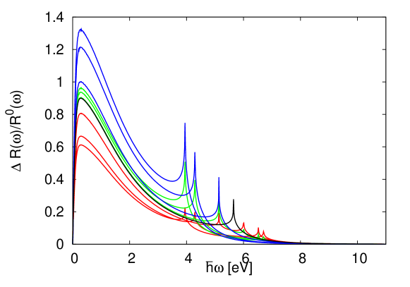
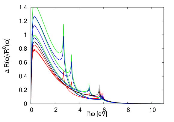
We consider light scattering across two media, with refraction index (), separated by a graphene monolayer. In the case of normal incidence, the reflectivity of such a system can be written as [20]
| (3) |
Assuming air on top of graphene, we have , whereas we can model the frequency dependence of the refraction index of the substrate through Cauchy’s law, as . In the case of SiO2, from a fit of data in Ref. [21], we find and eV. We evaluate as in Ref. [10].
Fig. 1 then shows our results for the relative reflectivity , where is the reflectivity of a single graphene monolayer with applied strain, between SiO2 and air, Eq. (3), and refers to the case without the insertion of a graphene layer. We specifically consider applied strain along the armchair () and zig zag () directions. Different colors refer to different polarization angles of the electric field (though always with normal incidence). In all cases, the black solid line refers to the case without strain, where the reflectivity does not depend on the electric field polarization angle.
While at large frequencies the reflectivity invariably tends to the case without graphene, differences are to be seen in the low-frequency range. In particular, the presence of logarithmic spikes can be associated with the proximity to the electronic topological transitions referred to above, their actual position depending on the strain modulus , as well as on the relative orientation of strain and electric field polarization angle .
References
- [1] P.R. Wallace, The Band Theory of Graphite, Phys. Rev. 71 (1947), p. 622.
- [2] A.H. Castro Neto, F. Guinea, N.M.R. Peres, K.S. Novoselov, and A.K. Geim, The electronic properties of graphene, Rev. Mod. Phys. 81 (2009), p. 000109.
- [3] C. Lee, X. Wei, J.W. Kysar, and J. Hone, Measurement of the Elastic Properties and Intrinsic Strength of Monolayer Graphene, Science 321 (2008), p. 385.
- [4] V.M. Pereira, A.H. Castro Neto, and N.M.R. Peres, Tight-binding approach to uniaxial strain in graphene, Phys. Rev. B 80 (2009), p. 045401 preprint arXiv:0811.4396.
- [5] F.M.D. Pellegrino, G.G.N. Angilella, and R. Pucci, Effect of impurities in high-symmetry lattice positions on the local density of states and conductivity of graphene, Phys. Rev. B 80 (2009), p. 094203 preprint arXiv.org/0909.1903.
- [6] F. Liu, P. Ming, and J. Li, Ab initio calculation of ideal strength and phonon instability of graphene under tension, Phys. Rev. B 76 (2007), p. 064120.
- [7] K.S. Kim, Y. Zhao, H. Jang, S.Y. Lee, J.M. Kim, K.S. Kim, J.H. Ahn, P. Kim, J. Choi, and B.H. Hong, Large-scale pattern growth of graphene films for stretchable transparent electrodes, Nature 457 (2009), p. 706.
- [8] Z.H. Ni, T. Yu, Y.H. Lu, Y.Y. Wang, Y.P. Feng, and Z.X. Shen, Uniaxial Strain on Graphene: Raman Spectroscopy Study and Band-Gap Opening, ACS Nano 2 (2008), p. 2301.
- [9] T.M.G. Mohiuddin et al., Uniaxial strain in graphene by Raman spectroscopy: peak splitting, Grüneisen parameters, and sample orientation, Phys. Rev. B 79 (2009), p. 205433.
- [10] F.M.D. Pellegrino, G.G.N. Angilella, and R. Pucci, Strain effect on the optical conductivity of graphene, Phys. Rev. B (accepted) … (2009), p. … preprint arXiv.org/0912.3614.
- [11] S. Reich, J. Maultzsch, C. Thomsen, and P. Ordejón, Tight-binding description of graphene, Phys. Rev. B 66 (2002), p. 035412.
- [12] M. Farjam and H. Rafii-Tabar, Comment on “Band structure engineering of graphene by strain: First-principles calculations”, Phys. Rev. B … (2009), p. … (submitted for publication; preprint arXiv:0903.1702).
- [13] O.L. Blakslee, D.G. Proctor, E.J. Seldin, G.B. Spence, and T. Weng, Elastic Constants of Compression-Annealed Pyrolytic Graphite, J. Appl. Phys. 41 (1970), p. 3373.
- [14] I.M. Lifshitz, Anomalies of electron characteristics of a metal in the high pressure region, Sov. Phys. JETP 11 (1960), p. 1130 [Zh. Eksp. Teor. Fiz. 38, 1569 (1960)].
- [15] Ya. M. Blanter, M.I. Kaganov, A.V. Pantsulaya, and A.A. Varlamov, The theory of electronic topological transitions, Phys. Rep. 245 (1994), p. 159.
- [16] A.A. Varlamov, G. Balestrino, E. Milani, and D.V. Livanov, The role of density of states fluctuations in the normal state properties of high- superconductors, Adv. Phys. 48 (1999), p. 655.
- [17] G.G.N. Angilella, E. Piegari, and A.A. Varlamov, Effects of an electronic topological transition for anisotropic low-dimensional superconductors, Phys. Rev. B 66 (2002), p. 014501.
- [18] G.G.N. Angilella, G. Balestrino, P. Cermelli, P. Podio-Guidugli, and A.A. Varlamov, Effects of strain-induced electronic topological transitions on the superconducting properties of La2-xSrxCuO4 thin films, Eur. Phys. J. B 26 (2002), p. 67.
- [19] G.G.N. Angilella, E. Piegari, R. Pucci, and A.A. Varlamov, Anisotropic low-dimensional superconductors close to an electronic topological transition, H.D. Hochheimer, B. Kuchta, P.K. Dorhout and J.L. Yarger, eds., , Vol. 48 of NATO Science Series Kluwer, Dordrecht, 2001.
- [20] T. Stauber, N.M.R. Peres, and A.K. Geim, Optical conductivity of graphene in the visible region of the spectrum, Phys. Rev. B 78 (2008), p. 085432.
- [21] I. Jung, M. Pelton, R. Piner, D.A. Dikin, S. Stankovich, S. Watcharotone, M. Hausner, and R.S. Ruoff, Simple Approach for High-Contrast Optical Imaging and Characterization of Graphene-Based Sheets, Nano Lett. 7 (2007), p. 3569.