Heterogeneous nucleation and metal-insulator transition in epitaxial films of NdNiO3
Abstract
We have investigated the temperature driven first order metal-insulator transition in thin films of NdNiO3 and have compared it with the bulk behavior. The M-I transition of thin films is sensitive to epitaxial strain and a partial relaxation of epitaxial strain creates an inhomogeneous strain field in the films which broadens the M-I transition. Both the thin film and the bulk samples exhibit non equilibrium features in the transition regime which are attributed to the presence of high temperature metallic phases in their supercooled state. The degree of supercooling in the thin films is found to be much smaller than in the bulk which suggests that the metal insulator transition in the thin film occurs through heterogeneous nucleation.
pacs:
64.60.My, 64.70.K-, 71.30.+h, 64.60.qjI Introduction
The study of first order metal-insulator (M-I) transition in transition metal oxides has been an active area of research for several decades now because of fundamental interest and exciting physical phenomena associated with these systems, for example hysteresis, slow dynamics, phase separation, colossal magnetoresistance etc.Imada ; Dagotto ; Morin ; Granados Whereas the presence of dynamical features has been reported in many early studies,Morin ; Granados an attempt to understand them and their dependence on the parameters controlling the M-I transition and their relationship with other associated phenomena such as hysteresis, phase separation has only started around the beginning of this century.Chaddah ; Chaddah1 ; Chaddah2 ; Devendra ; Devendra1 In these oxides, the family of rare earth nickelates (RNiO3, RLa) exhibits an M-I transition which can be tuned by application of internal or external pressure or strain.Medarde ; Obradors ; Canfield ; Kozuka ; Staub ; Ashutosh ; Novojilov ; Gatalan1 ; Gatalan ; Kaura ; Eguchi ; Conchon ; Ambrosinia ; Capon The M-I transition, the hysteresis and their connection to slow dynamics have been studied in detail in bulk NdNiO3 and PrNiO3.Granados ; Devendra ; Devendra1 In SmxNd1-xNiO3 and Nd0.7Eu0.3NiO3 thin films it has been observed that an increase in the film substrate lattice mismatch strain broadens the M-I transition and reduces the associated hysteresis.Ambrosinia ; Capon The physics of such behavior has not been explained so far. In this work we make an attempt to understand the effect of substrate strain on M-I transition and the differences in the M-I transition of the bulk and the thin films of NdNiO3 by performing a comparative study of a few relevant features of these systems.
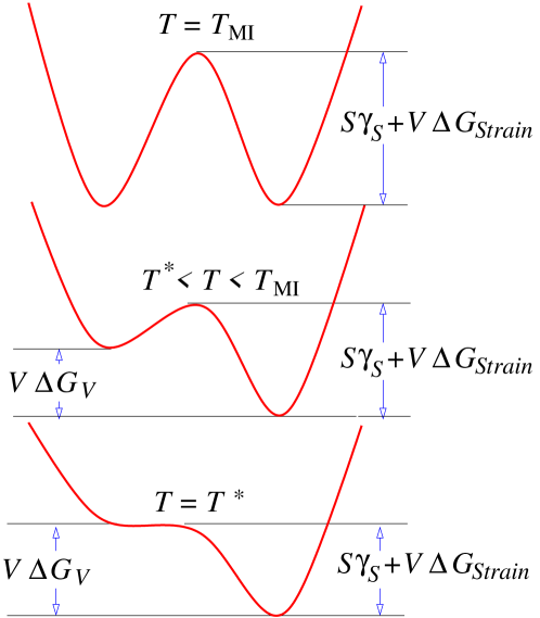
The existence of dynamical features in a first order phase transition (FOPT) system can be understood on the basis of the Landau formulation of mean field theory. In this theory, the free energy of the system is expressed in terms of an order parameter in the vicinity of the thermodynamic transition. In an FOPT system that undergoes a metal to insulator transition on cooling, at , the free energy of the system has two minima of equal depth separated by an energy barrier. One of the minima occurs at zero value of the order parameter and this corresponds to the high temperature metallic state and the other minimum occurs at a finite value of the order parameter and it corresponds to the low temperature insulating state.Chaikin See figure 1. On lowering the temperature further, the energy of the insulating state decreases and it becomes the stable state of the system while the metallic state exists as a supercooled (SC) metastable state. The high temperature metallic phase present in its SC state will remain in that state till it gains enough energy to overcome the free energy barrier () that separates it from the stable insulating state.Chaikin ; Chaddah For the energy barrier () is the energy required for the formation of a critical nucleus of the stable phase inside the SC phase. Once a critical nucleus is formed or in other words when the energy barrier is crossed, the rest of the SC phase will progressively transform or switch to the stable insulating state. At constant pressure and temperature, the energy required for the nucleation of a critical nucleus of volume and surface area is given as Porter :
| (1) |
where is the difference in the Gibb’s free energy per unit volume of SC metallic and stable insulating states, is the energy required per unit area for the formation of a metal-insulator interface and is the misfit strain energy per unit volume. At , is zero. So the critical nucleus at this temperature is essentially the complete metallic phase and and in equation 1 are equal to the volume and surface area of the metallic phase.endnote2 Below , increases monotonically on lowering the temperature which decreases and the size of critical nucleus. Thus the energy of nucleation is maximum at and decreases monotonically on lowering the temperature below . At a critical temperature , which is known as the limiting temperature of metastability, vanishes.Chaikin Now the SC metallic phase is free to switch to the stable insulating state and if the dynamics of the system is not frozen (i.e , being the temperature of kinetic arrest), then these SC regions will switch to the insulating state.Chaddah1 ; Devendra The presence of preferential sites for heterogeneous nucleation such as defects, interphase boundaries and free surfaces decreases and which in turn could decrease and the degree of maximum possible supercooling ().Porter In systems where such preferential sites for nucleation are missing, the SC phase will transform through homogeneous nucleation where usually is large and consequently the extent of maximum supercooling is also high.
In crystals quenched disorder such as lattice distortion, defects, strain fields and non-stoichiometry are usually induced during crystal growth. The presence of quenched disorder causes a local variation of the resulting in a broadening of the otherwise sharp first order M-I transition.Imry ; Soibel ; Chaddah2 ; Dagotto1 The local variation of will also cause a local variation of . Thus in a real system, while cooling, below the M-I phase transition temperature, we will have a collection of regions with definite and present either in metallic or insulating state. These regions switch from one state to the other as a single entity and we will refer to them as switchable regions (SR). In this set of SR’s there would be a fraction which will have . Of these, the SR’s which are in their metallic state, with , switch over to the insulating state stochastically giving rise to time dependence in physical properties of non-glassy and non-spin-glass type FOPT systems. This in turn results in a hysteresis between cooling and heating data.Devendra ; Devendra1
In this paper we report time and temperature dependent resistivity measurements on thin films of the FOPT system NdNiO3 and has compared the results with the bulk. Our results show that the M-I transition in the bulk is associated with a large hysteresis and strong dynamical effects while in thin films it has a small hysteresis and weak dynamical effects. We have discussed these results using the concepts of supercooling and nucleation which suggest that the energy () required for the nucleation of a critical insulating nucleus inside the metallic phase is much smaller for thin films compared to the bulk. This indicates that the M-I transition in the bulk occurs predominantly through homogeneous nucleation while the M-I transition in the films occurs predominantly through heterogeneous nucleation.
II Experimental Details and Results
II.1 Thin film deposition and structural analysis
High quality epitaxial films of NdNiO3 of thickness 200 nm were grown by pulsed laser deposition on {001} oriented single crystal NdGaO3 (NGO) substrates. An NdNiO3 pellet prepared by a low temperature method,Vassiliou and sintered at 1100 for 12 hours in an oxygen atmosphere, was used as the target for the thin film deposition. The energy density and pulse frequency for the deposition were 1.9 J/cm2 and 10 Hz respectively. The films were deposited at 0.3 mbar oxygen pressure and the substrate temperature was varied between 650-8000C. After the deposition the sample is cooled slowly at 1 bar O2 pressure. These films were characterized by resistivity measurements and the results are shown in figure 2(a). We found that the films are sensitive to the deposition temperature and that the films deposited at 700 0C have the best features. It has the smallest room temperature resistivity and shows the maximum relative change in resistivity on going from metallic to insulating state. We have used this film for the rest of the study. The sensitivity of NdNiO3 thin films to the deposition temperature has been reported earlier also.Kaura ; Eguchi Our thin film samples were also characterized by X-ray diffraction using CuK radiation on a PANalytical’s X’Pert PRO diffractometer and by scanning electron microscopy using a SUPRA 40VP FESEM and the data for the film deposited at 700 0C is shown in figure 2(b)-(f). The X-ray diffraction of NdNiO3 film has peaks only corresponding to {001} plane of NGO substrate which indicates that the NdNiO3 film is either highly <001> oriented or grown epitaxially on NGO substrate with out of pane lattice parameter =7.710 Å and =7.573 Å. The FWHM of the (004) peak of the thin films is 0.31 degree which is higher than that of bulk samples (0.18 degree). This gives the average grain size of thin films as 60 nm which is smaller than that of bulk sample (132 nm).
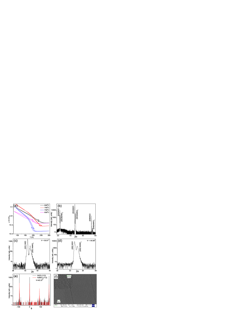
The in plane lattice parameter of thin films were obtained by the asymmetric scan of the (200) and (022) planes. Table 1 shows the lattice parameters , , , Ni-O-Ni bond angle and unit cell volume for thin films and the bulk sample. A comparison of the lattice parameters , , and show that the NdNiO3 thin films are under in-plane tensile strain and out-of-plane compressive stress because of NdGaO3 substrate. The increase in the in-plane lattice parameters and of thin films should have decreased the out-of-plane lattice parameter in such a way that the unit cell volume remains conserved. But this is not the case and the thin films have a higher unit cell volume compared to bulk NdNiO3. The unit cell volume of the NdNiO3 depends on the oxygen vacancies and it increases on increasing the vacancies.Tiwari ; Nikulina This suggest that in thin films a partial stress relaxation has happened by the formation of oxygen vacancies. Similar chemical stress relaxation has been observed in SmNiO3 films deposited on SrTiO3 substrates.Conchon The X-ray scan measurement were performed to check the epitaxy of the thin films. In figure 2(e) we show the scan plot of (112) plane of NdNiO3 film deposited on (001) oriented NGO substrate. We get four equal spaced peaks for NdNiO3 which are aligned with that of NGO. This clearly indicates the epitaxial growth of NdNiO3 on NGO substrate. Figure 2(f) shows the scanning electron micrograph of the film surface. The film surface is formed of tiny (001) oriented grains. The size of these grains is much smaller than that of bulk samples.endnote The surface of the film shows few nano-scale line cracks. These cracks usually form due to relaxation of the film-substrate lattice mismatch strain and the differential contraction of the film and substrate during the cooling process after the thin film deposition.Freund ; Kazuki ; Copetti ; Tian
| a (Å) | b (Å) | c (Å) | (deg.) | (Å3) | |
|---|---|---|---|---|---|
| Bulk | 5.3888 | 5.3845 | 7.6127 | 157.5 | 220.89 |
| Thin film | 5.406 | 5.447 | 7.573 | 155.4 | 223.00 |
| NdGaO3 | 5.431 | 5.499 | 7.710 | - | 230.26 |
II.2 Transport measurements and results
Figure 3 shows the normalized electrical resistivity of our best NdNiO3 thin film as a function of temperature. The rate of temperature variation was fixed at 2 Kmin-1 for all the experiments. The resistivity is multiple valued, the cooling and heating data differ from each other and form a hysteresis loop. The resistivity plot indicates that the NdNiO3 thin film begins to undergo a first order metal-insulator transition at 215 K. In the same figure we have also plotted the resistivity of bulk NdNiO3 for easy comparison. We can see that the beginning of the M-I transition in thin films is about 15 K higher than that of bulk sample. The M-I transition temperature, metallic resistivity and the ratio of metallic to insulating resistivity of NdNiO3 thin films depends on the film thickness, choice of substrate and the deposition condition.Ashutosh ; Gatalan1 ; Gatalan ; Kozuka ; Conchon ; Kaura ; Eguchi For NdNiO3 thin films deposited on (001) oriented NGO substrate, the higher value of M-I transition temperature than the bulk has also been reported earlier and it is attributed to in plane tensile strain and out of plane compressive stress present in these films.Eguchi The epitaxial strain of the films decreases the Ni-O-Ni superexchange angle of the films compared to the bulk sample. See table 1. This results in a bandwidth narrowing which subsequently increases the M-I transition temperature of the films. Similar effects has been observed in the bulk samples where an increase in distortion (by decreasing the rare earth ionic radius) increases the .Medarde The higher value of M-I transition temperature in thin films and the comparison of lattice parameters show that the NdNiO3 thin films are more distorted compared to the bulk.
At room temperature the resistivity of the thin film is 2.1(1) mcm which is higher than the resistivity of bulk sample 1.2(2) mcm. The ratio of insulating to metallic resistivity of thin film is about 60 times lower than that of bulk NdNiO3. See figure 3. The higher metallic resistivity of thin films may be attributed to their smaller grain size and also to the defects (line cracks and vacancies) formed by partial stress relaxation.Fu ; Gupta ; Kazuki ; Copetti ; Tian ; Conchon ; Nikulina The large density of grain boundaries and defects enhances the electron scattering which increases the resistivity of the metallic state. On the other hand, in the insulating state the higher density of grain boundaries and vacancies create defect levels in the band gap which lowers the insulating resistivity of the films.Nikulina ; Shockley ; Victor ; Mckeena ; Brassard Similar effect of grain size dependence has also been observed in VO2 thin films.Brassard In the cooling run the M-I transition of bulk NdNiO3 is centered at 155 K with a spread of about 90 K while in the heating run the M-I transition is relatively sharp and has a width of about 10 K. Below 110 K the heating and cooling data merge and the log versus plot is linear. In the case of thin film we note that the M-I transition is broader and it spreads over a temperature range of about 120 K. In contrast to bulk, the width of M-I transition for thin films is nearly the same for cooling and heating runs. We further note that the amount of hysteresis in the films is much less than that of the bulk system. Below 95 K the heating and cooling data merge and the log versus plot is linear.
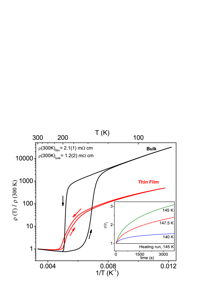
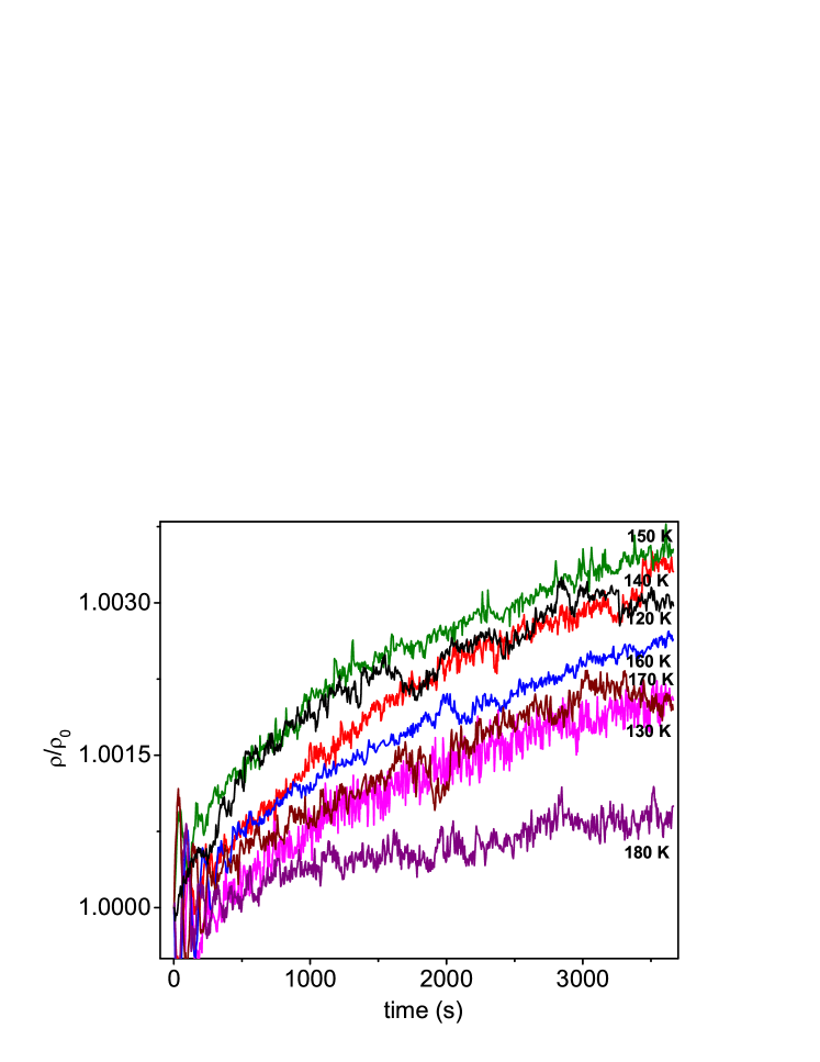
Figure 4 exhibits a subset of the time dependent resistivity data for the thin films in the cooling run. The time dependent resistivity data was recorded using the following protocol. The sample was cooled from 250 K (>) to the temperature of interest and the resistivity of the sample was recorded as a function of time. Endnote The data is presented in the form of so that the values are normalized to unity at t=0 for easy comparison. We found that below 200 K the resistivity of the film increases with time. The presence of time dependence in resistivity indicates that the system is not in thermodynamic equilibrium. These curves were fitted to the stretched exponential function
| (2) |
where , , and are fit parameters. The thin film time dependent data is noisy compared to the bulk samples and the quality of fitting is not as good as in bulk samples. See Table 2. A maximum relative increase in resistivity of about 0.35 % occurs at around 150 K.Endnote1 The relative increase in the resistivity () of the thin films of NdNiO3 (maximum 0.35 % in one hour) is much less than that observed in polycrystalline NdNiO3 (maximum 200 % in one hour at 145 K . See inset of figure 3 and Ref. Devendra, ). No detectable time dependence was observed below 95 K and in the subsequent heating run. The fitting parameter of thin films () is more close to 1 compared to bulk samples (), which indicates that at the temperature of relaxation the SR’s of thin films have a narrow distribution of in comparison to bulk.
| # | T(K) | (s) | ||||
|---|---|---|---|---|---|---|
| 1 | 120.0 | 0.0043(2) | 1.7(1) | 0.64(3) | 4.44 | 0.97309 |
| 2 | 130.0 | 0.0038(4) | 2.7(6) | 0.75(6) | 6.63 | 0.94336 |
| 3 | 140.0 | 0.0055(3) | 3.3(3) | 0.78(3) | 1.86 | 0.98603 |
| 4 | 150.0 | 0.0043(3) | 2.5(2) | 0.79(3) | 1.66 | 0.98584 |
| 5 | 160.0 | 0.006(3) | 6(7) | 0.49(8) | 2.54 | 0.93284 |
III Discussion
III.1 Behavior of electrical resistivity and nucleation of insulating phases
As shown in Figure 3 the M-I transition for bulk NdNiO3 in cooling run starts from 200 K, and on lowering the temperature more and more regions (SR’s) of the sample transform to the insulating state. Below 110 K, cooling and heating data merge and it follows the band gap model of insulators which indicates that most of the SR’s have completed their transition to the insulating state. The resistivity of the system exhibits a large time dependence (maximum 200 %) in the cooling run which suggest that a large fraction of SR’s are present below their respective in their SC metastable state. The time dependent effects persists down to 110 K which shows that of SR’s are distributed in the range of 200 K to 110 K.Devendra ; Devendra1 In the heating run the M-I transition is narrow, is centered around 195 K and has a width of about 10 K. The time dependence of resistivity in the heating run is negligible compared to the cooling run. This rules out the possibility of superheating and suggests that the temperature where an SR changes from insulating to metallic state in a heating run is the of that SR. The broadening of M-I transition in the heating run is due to disorder induced variation of local . So in the bulk sample, local has a variation of 200-190 K while the has a variation from 200-110 K. The existence of metallic SR’s in their SC state much below their respective (a high degree of supercooling) suggests that in cooling runs most of the SR’s transform from metallic to insulating state through homogeneous nucleation.
In the case of thin films the M-I transition is much broader than in the bulk, it starts from 215 K and occurs over a temperature range of about 120 K. The higher broadening of the M-I transition in the films is possibly related to epitaxial strain of the films. During the epitaxial growth of the films if the elastic energy of the film due to substrate lattice mismatch strain exceeds the critical energy required for the creation of defects, then the film partially relaxes its elastic energy by formation of defects.Freund The defects can be of mechanical(eg. cracks, stacking faults) or chemical (eg. creation of oxygen vacancies) in nature.Kazuki ; Copetti ; Tian ; Conchon The elastic energy depends on the amount of lattice mismatch and the thickness of the film and for a film-substrate combination, above a critical thickness or strain, defects will be formed to reduce the elastic energy. The variation of epitaxial strain across the thickness of the film is not uniform, and in general it is pronounced close to the thin film substrate interface and relaxes on moving towards the free surface.Conchon ; Boulle Thus the formation of defects causes a variation of strain field inside the films. This will results in the local variation of inside the films and it will broaden the metal to insulator transition of the films. This effect has been seen experimentally in (a) thickness dependent studies of NdNiO3, SmNiO3 and VO2 thin films where the thinner films exhibits a sharper M-I transition compared to thick films.Gatalan ; Conchon ; Kazuki (b) SmxNd1-xNiO3 thin films where the increase in Sm content results in broader M-I transition.Ambrosinia In our thin films the occurrence of partial stress relaxation by formation of defects has already been discussed in section II.1, and it shows itself in the form of line cracks and increase in unit cell volume. See figure 2(f) and table 1. This is a pointer to the presence of inhomogeneous strain fields in the film which causes a local variation of and a broad M-I transition.
The broadness of the M-I transition and the nature of vs curve of the film are nearly the same for the heating and cooling runs. This means that for most of the SR’s the temperatures where it transforms from metallic to insulating state in cooling run and from insulating to metallic state in heating run, are nearly the same. In the cooling run the presence of time dependence suggest that the switching happens somewhere between and , stochastically. Since we did not find any time dependence in heating run, the switching temperature of an SR in a heating run is its local . Thus the similarity in vs curves in heating and cooling runs of the film suggest that and are very close for most of the SR’s. The close value of and decreases the temperature range where an SR can exist in its SC state in the cooling runs. This will result in a decrease in the fraction of SR’s present in their SC state compared to the bulk. Thus we will have a smaller number of SR’s available to switch from SC metallic state to insulating state with time and hence we will get a weak time dependence and a small hysteresis in thin films which is in accordance with the observations. See Figures 3 and 4.
The and for most of the SR’s in thin films are nearly the same and thus the films have a small degree of supercooling while the bulk samples exhibit a high degree of supercooling. This shows that energy of nucleation () for the films is greatly reduced, which suggest that at the local level the M-I transition in the films is occurring through heterogeneous nucleation.
III.2 Preferred sites for heterogeneous nucleation
The preferential sites for nucleation are the free surface, the thin film substrate interface, stacking faults, dislocation and vacancies and in general it is found that the energy of nucleation () is minimum for free surface and is maximum for homogeneous sites.Porter . For the NdNiO3 thin films on (001) oriented NGO substrate, the probable places of nucleation are the free surface of the film, the defects, and the film substrate interface(because the high in-plane tensile strain of the interface layers favor the existence of insulating state). The formation of a critical nucleus of insulating phase at the defects will have a smaller , the nucleation at the free surface will have smaller and , and the nucleation at interface will have a smaller compared to other regions of the films. Thus at a temperature , in the set of SR’s that have the same M-I transition temperature, those located at the free surface, the defects and the interface will have a smaller energy of nucleation and this suggest that these sites will act as preferred sites for heterogeneous nucleation. Since our thin films have a high density of heterogeneous nucleation sites (high concentration of defects, large free surface area and favorable interface), the number of SR’s located at these sites will be high and these SR’s will transform from metallic to insulating state through heterogeneous nucleation. The transformation of an SR from the SC metastable state to the insulating state occurs through a release of excess energy.Porter This excess thermal energy will be absorbed by the nearby SC SR’s and it may help them in forming the critical nucleus of insulating phase. Further the surfaces of already transformed SR’s have the same structure as that of critical nucleus, their surfaces will partially reduce the surface energy () required for formation of a critical nucleus in the adjacent SC SR’s. Thus the transformed SR’s at the heterogeneous nucleation sites will act as preferred sites for the adjacent SR’s and so on.
For SmxNd1-xNiO3 thin films, an increase in the Sm content increases the in-plane tensile strain and out-of-plane compressed stress. The resistivity measurements on these samples have shown that increase in Sm content broadens the M-I transition and decreases the hysteresis.Ambrosinia The reason for such behavior was not clear and now it can be understood using the concepts developed in this work. On increasing the Sm content, the elastic strain energy of the film will increase and the film will try to minimize it by increasing the number of defects. This results in varying stress field and will cause a local variation of inside the films and thus the broadening of the M-I transition. Further these enhanced defects sites will increase the number of heterogeneous nucleation sites in the films which will reduce the degree of supercooling of a fraction of SR’s and it will result in smaller hysteresis. Similar explanations can be given for the case of Nd0.7Eu0.3NiO3 thin films.
IV Conclusion
In conclusion our experimental results and discussion on NdNiO3 thin films suggest that the physical properties of the films are sensitive to deposition condition and film substrate lattice mismatch strain. The elastic strain energy of the thin films is partially relaxed by formation of defects which broadens the M-I transition of the films. The thin films and the bulk both exhibit non equilibrium features in the transition regime which are attributed to the existence of high temperature metallic phases in their supercooled metastable state. The degree of supercooling in the thin films is found to be much smaller than in the bulk samples whcih indicates that the M-I transition in the bulk occurs through homogeneous nucleation while the M-I transition in the films occurs through heterogeneous nucleation. Our analysis show that in comparison to the bulk samples, the thin films have a higher density of heterogeneous nucleation sites and hence the majority of the thin film transforms from metallic to insulating state through heterogeneous nucleation. Using these ideas we have also explained the higher broadening and decrease in hysteresis in M-I transition of SmxNd1-xNiO3 and Nd0.7Eu0.3NiO3 thin films.
V Acknowledgements
DK thanks the University Grants Commission of India for financial support. RCB acknowledges the research grant from Indo-French center for promotion of Advanced Research.
References
- (1) M. Imada, A. Fujimori and Y. Tokura, Rev. Mod. Phys. 70, 1039 (1998).
- (2) E. Dagotto, Nanoscale phase separation and Colossal Magnetoresistance (Springer, Berlin, 2002).
- (3) F. J. Morin, Phys. Rev. Lett. 3, 34 (1959).
- (4) X. Granados, J. Fontcuberta, X. Obradors and J. B. Torrance, Phys. Rev. B 46, 15683 (1992).
- (5) P. Chaddah and S. B. Roy, Phys. Rev. B 60, 11926 (1999).
- (6) P. Chaddah cond-mat/0109310v1.
- (7) P. Chaddah, K. Kumar, and A. Banerjee, Phys. Rev. B 77, 100402(R) (2008).
- (8) D. Kumar, K. P. Rajeev, J. A. Alonso, and M. J. Martínez- Lope, J. Phys: Condensed Matter 21, 185402 (2009).
- (9) D. Kumar, K. P. Rajeev, J. A. Alonso and M. J. Martínez- Lope, J. Phys: Condensed Matter 21, 485402 (2009).
- (10) M. L. Medarde, J. Phys.: Condens. Matter 9, 1679 (1997).
- (11) X. Obradors, L. M. Paulius, M. B. Maple, J. B. Torrance, A. I. Nazzal, J. Fontcuberta, and X. Granados, Phys. Rev. B 47, 12353 (1993).
- (12) P. C. Canfield, J. D Thompson, S. W. Cheong, and L. W. Rupp, Phys. Rev. B 47, 12357 (1993).
- (13) M. A. Novojilov, O. Yu. Gorbenko, I. E. Graboy, A. R. Kaul, H. W. Zandbergen, N. A. Babushkina, and L. M. Belova, Appl. Phys. Lett. 76, 2041 (2000).
- (14) U. Staub, G. I. Meijer, F. Fauth, R. Allenspach, J. G. Bednorz, J. Karpinski, S. M. Kazakov, L. Paolasini, and F. d’Acapito, Phys. Rev. Lett. 88, 126402 (2002).
- (15) A. Tiwari, C. Jin, and J. Narayan, Appl. Phys. Lett 80, 4039 (2002).
- (16) G. Catalan, R. M. Bowman, and J. M. Gregg, J. Appl. Phys. 87, 606 (2000).
- (17) G. Catalan, R. M. Bowman, and J. M. Gregg, Phys. Rev. B 62, 7892 (2000).
- (18) Y. Kozuka, T. Susaki, and H. Y. Hwang, Appl. Phys. Lett. 88, 142111 (2006).
- (19) D. Kaura, J. Jesudasanb, and P. Raychaudhuri, Solid State Communications 136, 369 (2005).
- (20) F Conchon, A. Boulle, R. Guinebreti‘ere, E. Dooryh´ee, J-L Hodeau, C. Girardot, S. Pignard, J. Kreisel and F. Weiss, J. Phys: Condensed Matter 20, 145216 (2008).
- (21) R. Eguchi, Y. Okamoto, Z. Hiroi, S. Shin, A. Chainani, Y. Tanaka, M. Matsunami, Y. Takata, Y. Nishino, K. Tamasaku, M. Yabashi, and T. Ishikawa, J. Appl. Phys. 105, 056103 (2009).
- (22) A. Ambrosinia and J.-F. Hamet, Appl. Phys. Lett 82, 727 (2003).
- (23) F. Capon, P. Laffez, J.-F. Bardeau, P. Simon, P. Lacorre, and M. Zaghriouid, Appl. Phys. Lett 81, 619 (2002).
- (24) P. M. Chaikin and T. C. Lubensky, Principles of Condensed Matter Physics (Cambridge University Press 1998) chapter 4.
- (25) D. A. Porter and K. E. Easterling, Phase Transformations in Metals and Alloys (Champan and Halls (1996)) Chapter 4 and 5.
- (26) By the phrase ’complete metallic phase’ we mean a region which switches from metallic to insulating state as a whole. It can be a crystallite or a portion of that (for more detail see Ref. Devendra, ).
- (27) Y. Imry and M. Wortis, Phys. Rev. B 19, 3580 (1979).
- (28) A. Soibel, E. Zeldov, M. Rappaport, Y. Myasoedov, T. Tamegai, S. Ooi, M. Konczykowski and V. B. Geshkenbein 2000 Nature 406 282.
- (29) E. Dagotto 2005 Science 309 257.
- (30) J. K. Vassiliou, M. Hornbostel, R. Ziebarth, and F. J. Disalvo, J. Solid State Chem. 81, 208 (1989).
- (31) A. Tiwari and K.P. Rajeev, Solid State Communications 109, 119 (1999).
- (32) I.V. Nikulina, M.A. Novojilova, A.R. Kaulb, S.N. Mudretsovab, and S.V. Kondrashov, Mater. Res. Bull. 39, 775 (2004).
- (33) From FESEM images of the bulk sample and thin films, a rough estimate of the grain size at the surface can be made. It is about 250 nm for bulk samples and about 50 nm for thin films. This roughly agrees with the values obtaine from X-ray peak width using Scherr formula.
- (34) P. Lacorre, J. B. Torrance, J. Pannetier, A. I. Nazzal, P. W. Wang, and T. C. Huang, J. Solid State Chem. 91, 225 (1991).
- (35) K. Hayashi, G. Demazeau, M. Pouchard, Revue de chimie minerals (18), 148 (1991. The Ni-O-Ni bond angle is given by the relation , where Cos.
- (36) K. Nagashima, T. Yanagida, H. Tanaka, and T. Kawai, Phys. Rev. B 74, 172106 (2006).
- (37) A. Copetti, J. Schubert, W. Zander, H. Soltner, U. Poppe, and Ch. Buchal, J. Appl. Phys. 73, 1339 (1993).
- (38) Y. J. Tian, S. Linzen, F. Schmidl, A. Matthes, H. Schneidewind, and P. Seidel, Thin Solid Films 338, 224 (1999).
- (39) L. B. Freund and S. Suresh, Thin Film Materials: Stress, Defect Formation and Surface Evolution (Cambridge University Press 2003) chapter 1.
- (40) Yonglai Fu, Appl. Phys. Lett. 77, 118 (2000).
- (41) A. Gupta, G. Q. Gong, G. Xiao, P. R. Duncombe, P. Lecoeur, and P. Trouilloud, Y. Y. Wang, V. P. Dravid, and J. Z. Sun, Phys. Rev. B 54, 15629 (1996).
- (42) W. Shockley and W. T. Read, Phys. Rev. 87, 835 (1952).
- (43) P. Victor, J. Nagaraju, and S. B. Krupanidhi, Proceedings of 13th IEEE International Symposium on Applications of Ferroelectrics, page 207 (2002).
- (44) K. P. Mckeena and A L. Shluger, Nature Materials 7, 860 (2008).
- (45) D. Brassard, S. Fourmaux, M. Jean-Jacques, J. C. Kieffer, and M. A. El Khakania, Appl. Phys. Lett. 87, 051910 (2005).
- (46) The details of measurement procedure is given in Ref. Devendra, .
- (47) The magnitude of time dependence in resistivity and its variation with temperature depends on the volume fraction of SC metallic SR’s, their energy of nucleation , and the temperature of percolation threshold. The resistivity of the system is connected by the metallic volume fraction by McLachlan GEM theory. We will get a higher timedependence in the volume when the volume fraction of SC SR’s having their within a few Kelvin of the temperature of measurement () is high. The detailed calculations for the bulk NdNiO3 has been reported in Ref. Devendra, .
- (48) A. Boulle, R. Guinebretière, and A. Dauger, J. Appl. Phys. 97, 073503 (2005).