Present address: ]Physics Department, Blackett Laboratory, Imperial College London, Prince Consort Road, London SW7 2BZ, United Kingdom
Domino plasmons for subwavelength terahertz circuitry
Abstract
A new approach for the spatial and temporal modulation of electromagnetic fields at terahertz frequencies is presented. The waveguiding elements are based on plasmonic and metamaterial notions and consist of an easy-to-manufacture periodic chain of metallic box-shaped elements protruding out of a metallic surface. It is shown that the dispersion relation of the corresponding electromagnetic modes is rather insensitive to the waveguide width, preserving tight confinement and reasonable absorption loss even when the waveguide transverse dimensions are well in the subwavelength regime. This property enables the simple implementation of key devices, such as tapers and power dividers. Additionally, directional couplers, waveguide bends, and ring resonators are characterized, demonstrating the flexibility of the proposed concept and the prospects for terahertz applications requiring high integration density.
I Introduction
Electromagnetic radiation in the terahertz (THz) regime is a central resource for many scientific fields such as spectroscopy, sensing, imaging, and communications. We are currently witnessing the take off of THz technologies ferguson02 ; siegel02 ; tonouchi07 with applications as diverse as astronomy withington04 , medicine siegel04 , or security federici05 . Within this general endeavour, the building of compact THz circuits would stand out as an important accomplishment. This requires the design of THz waveguides carrying tightly confined electromagnetic (EM) modes, preferably with subwavelength transverse cross section. Besides circuit integration and compact device design, sub- localization may be advantageous for waveguide THz time-domain spectroscopy zhang04 and non-diffraction-limited imaging cunningham08 . Although a number of structures has been put forward, none of them passes all the following requirements. First, structures should be easily manufactured and, if possible, planar and monolithic. Second, as above motivated, subwavelength transverse size is also needed. Finally, absorption and bend losses should be small, and the waveguides sufficiently versatile for the design of key functional devices. Particularly important are in/out-couplers since they work as the interface to external waves. In this context, compact tapers able to laterally compress the modes down to the sub- level seem essential.
With these requirements in mind it is illuminating to compare optical waveguides with those proposed for the THz range. Optical fiber modes exhibit a cut-off diameter such that fibers cannot be of subwavelength size and, moreover, modal size grows as this cut-off is approached. In the THz regime dielectric wires jamison00 meet the same limitation. The photonic crystal fiber approach han02 shares the inability of sub- confinement, and low-index discontinuity waveguides nagel06 perform better regarding modal size but are neither planar nor monolithic. Metals are an alternative when operating at optical frequencies because surface plasmon polaritons (SPPs) propagating on flat metal-dielectric interfaces provide subwavelength confinement in the direction perpendicular to the surface. This metallic route has been tried for the THz regime, but the corresponding EM modes, known as Zenneck or Sommerfeld waves, loose their confined character at these frequencies jeon06 ; wang04 .
Geometrically-induced surface plasmons pendry04 supported by periodically corrugated metallic surfaces overcome the low localization of Zenneck waves. A number of waveguiding structures based on this concept has been already suggested zhu08 ; maier06 ; fernandez09a ; fernandez09b , but they have failed to meet simultaneously all the above mentioned requirements. In this work we present structures based on this metamaterial approach that, thank to their superior properties, fulfill the requisite easy fabrication, subwavelength confinement, low loss, and device flexibility.
II Results
The basic structure consists of a periodic arrangement of metallic parallelepipeds standing on top of a metallic surface and resembling a chain of domino pieces, see inset of Fig. 1(a). In contrast with corrugated wires maier06 , this is a planar and monolithic system and should not pose significant manufacturing problems, its geometry being much simpler than corrugated V-grooves fernandez09a or wedges fernandez09b . The properties of its guided modes, hereafter referred to as domino plasmons (DPs), are mainly controlled by the geometric parameters defining the dominoes, i.e., periodicity , parallelepiped height , lateral width , and inter-domino spacing .
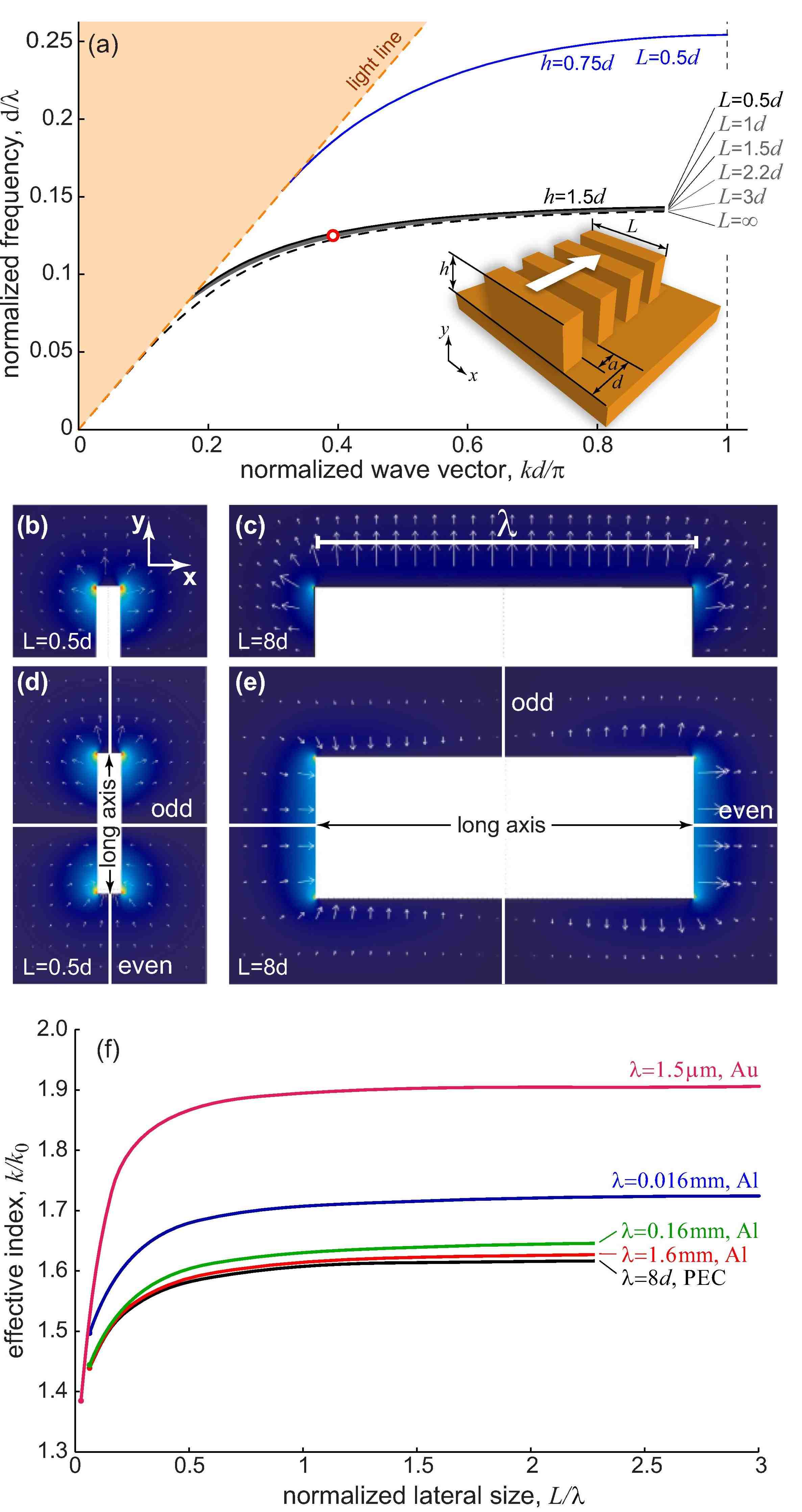
First, the basic properties of DPs are described starting with the dispersion relation. To gain physical insight we model the metal as a perfect electric conductor (PEC). Later, realistic metals will be considered, letting us to discern what is the frequency regime where DPs display the most promising behaviour. The numerical technique is described in the Methods section. Due to the simple scaling properties of PECs, we choose the periodicity as the length unit. The value of is not critical for the properties of DPs and is set as in this work. DP bands present a typical plasmonic character, i.e., they approach the light line for low frequencies and reach a horizontal frequency limit at the edge () of the first Brillouin zone (Fig. 1(a), notice that only fundamental modes are plotted). In all cases DP modes lie outside the light cone, a fact that explains their non-radiative character. While the limit frequency of SPPs for large is related to the plasma frequency, the corresponding value for DPs is controlled by the geometry. The influence of the height is clear: the band frequency rises for short dominoes (, blue line) as compared with that of taller ones (, black line). This can be understood as follows. When , dominoes become a one-dimensional (1D) array of grooves which supports a geometrically-induced plasmon mode. Its dispersion relation is represented, for , with a dashed line in Fig. 1(a). An approximation for the dispersion relation in this limit, neglecting diffraction effects and for , is garciavidal05
| (1) |
where is the modal wave vector, , and the component of the wave vector inside the grooves, , is related with the corresponding and components by . The EM fields inside the grooves are independent of and for the chosen longitudinal polarization and thus , . This means that Eq. 1 presents an asymptote for or, in other words, for a normalized frequency . Such dependence with explains the behaviour observed in Fig. 1(a). For , the value chosen in the rest of the paper, this estimation for the limit normalized frequency provides a figure of about , not far from the numerically computed value of .
The most striking characteristic of DPs is their behaviour when the lateral width is changed. All bands in the range lie almost on top of each other (Fig. 1(a), grey curves). In other words, the modal effective index, , is rather insensitive to lateral width. If we now look at the numerically computed dispersion relations of Fig. 1(a) in the light of Eq. 1, it seems that for a wide range of . Remarkably, the bands remain almost unchanged even for , whose modal size is well inside the subwavelength regime, as observed in the field distribution plotted in panel (b) for a narrow structure (). Notice that the white bar representing in panel (c) is valid for panels (b)-(d), and the modal size, defined as the FWHM of the modulus of the Poynting field distribution, is for panel (b). The described behaviour is to be contrasted with that of conventional plasmonic modes in the optical regime for which sub- lateral confinement is not a trivial issue verhagen09 . When the lateral size of the structure supporting such modes becomes subwavelength, either the modal size grows, or the effective index increases. This is best illustrated for a free standing metallic stripe berini00 . A stripe of large lateral width essentially supports an SPP mode but, as this width is decreased and becomes sub-, the plasmonic modes that are not cut-off become either highly confined but quite lossy, or otherwise highly delocalized.
The insensitivity of DPs to lateral size, which constitutes the foundation of some of the devices presented later, can be linked in an intuitive way to the structure geometry. The key role played by the metallic substrate can be explained by comparison of DPs and the modes of a Yagi-Uda structure, i.e., a periodic array of free standing metallic rods sengupta59 ; krenn99 ; maier01 . For small the dispersion of DPs of height is identical to that of the fundamental mode of a Yagi-Uda structure of height , and the field of the DP is simply the upper half of the fundamental mode of a rod array of height , see Figs. 1(b) and (d). For large this correspondence does not hold anymore, as demonstrated by comparison of panels (c) and (e) which display completely different symmetries. For dominoes, a mode with the same symmetry as the Yagi-Uda mode shown in panel (e) is forbidden because the horizontal electric field has to be zero at the metallic ground. This mode suppression is critical because the frequency of the fundamental mode of a Yagi-Uda structure, which is essentially controlled by the length of the long axis of the rods, is very sensitive to the lateral width , being very different for short vertical rods and long horizontal rods. It is similarly important that the air gaps between the dominoes are laterally open. Let us imagine that, instead of being open, they were laterally closed by PEC walls. Since the electric field inside the gap points longitudinally from one domino to the next one, it should then vanish at both PEC lateral walls, giving a cosine-like dependence. It is then clear that the mode frequency should increase when the lateral size is decreased, arriving to the conclusion that the modes of such an structure have -sensitive bands. In contrast, for DPs the boundary conditions at the laterally open gaps are more akin to perfect magnetic walls, and the corresponding field is approximately -independent inside the air gaps even when .
Let us scrutinize in more detail the role played by the lateral dimension , considering now realistic metals and paying attention to the spectral regime. The periodicity is chosen to set the operating wavelength in the desired region of the EM spectrum, and is varied in the range , while the remaining parameters are kept constant (, ). Aluminum is selected for low frequencies, where metals behave almost like PECs. In order to work at , providing an operating angular frequency of the order of 1 THz, we first consider . The evolution of the modal effective index as a function of the lateral dimension normalized to the wavelength is plotted in Fig. 1(f). The curves corresponding to a PEC (black line) and aluminum at (red line) are, as expected, almost identical. We can now quantify the sensitivity of the effective index to , its variation being only about 12% even when goes from to , well inside the sub- regime. The rapid variation of when can be understood with the help of Eq. 1. In this limit the EM fields start to be -dependent inside the air gaps, as verified by inspection of the fields (not shown here), letting us to conclude that and consequently . Then, if we assume that Eq. 1 is still valid in this limit, it predicts that the modal effective index is reduced when . To investigate the performance of DPs at higher frequencies, the structures have been scaled down by factors 1/10 and 1/100. The fact that the curves corresponding to (green line) and (blue line) do not lie on top of the previous ones is a signature of the departure of aluminum from the PEC behaviour. Nevertheless, even at , the variation of the effective index is still smaller than 15%, a property that can be exploited for taper design in the far infrared, albeit with slightly reduced performance as compared with the THz case. When the operating frequency moves to the telecom regime (, magenta line) the variation of the effective index is much larger (about 38%). Let us mention in passing that, for this wavelength, we have used gold because it has lower loss than aluminum, and that the geometric scaling had to be different (the periodicity is now ) because with the same simple scaling as before no DP mode is supported due to the value of the permittivity of gold. The important message of panel (f) is that, although a variation of begins to be noticeable when the lateral dimension goes below , DP bands are fairly insensitive to in the range when operating at low frequencies. Such property has, to our knowledge, never been reported for geometrically-induced plasmon modes in corrugated wedges, channels, or wires.
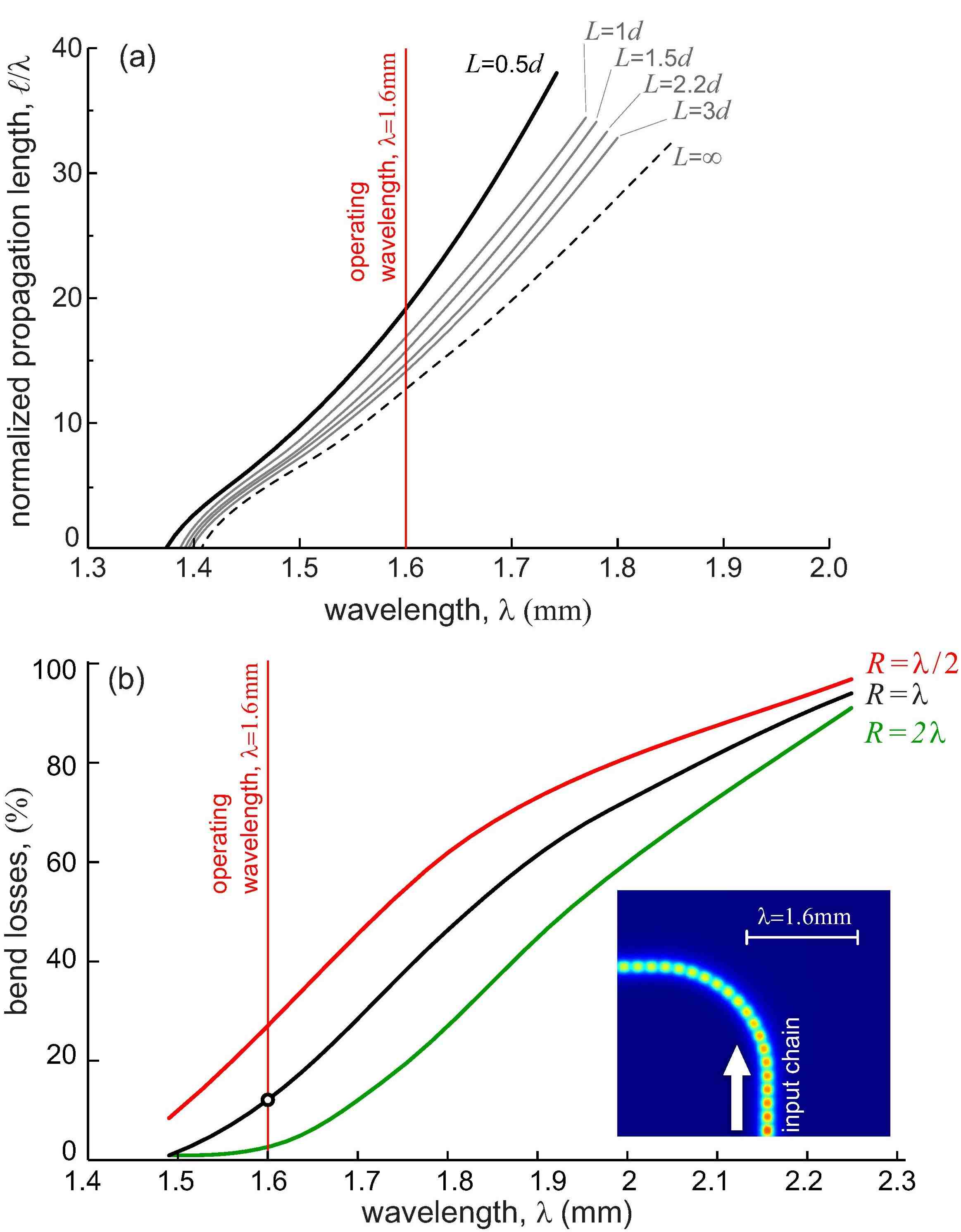
Now that we have identified the THz range as the most promising operation regime, we will characterize the corresponding absorption (ohmic) and bending losses. Figure 2(a) displays the propagation length () of DPs as a function of wavelength for various widths ( for all curves). The only source of damping in the domino structure is absorption by the metal as no radiation losses occur in such straight waveguide. Propagation length is very short for small , when the Brillouin zone edge is reached, but it rises for increasing wavelength as the dispersion curve approaches the light line. Several lateral widths are considered and it is observed that DPs in structures of smaller travel longer distances before being damped. The radiation losses occurring in a waveguide of with a 90 degree bend are analyzed in panel (b). In this case the metal is modelled as a PEC for easier evaluation of radiation losses. Data for three radii of curvature of the bend, , are presented. In all three cases, losses are low for small but they grow as the wavelength is increased and the modal wave vector approaches . The dependence with the radius of curvature of the bend is not surprising either, radiation losses being higher for smaller radius of curvature. Consideration of absorption and bending losses suggests that can be an appropriate operating wavelength. For and , the modal size is , i.e., about . The propagation length is about , much larger than the size of the devices presented later, and the bend loss for is reasonably low, about 10%. Notice that for corrugated V-grooves, the bend loss for is around 50% fernandez09a .
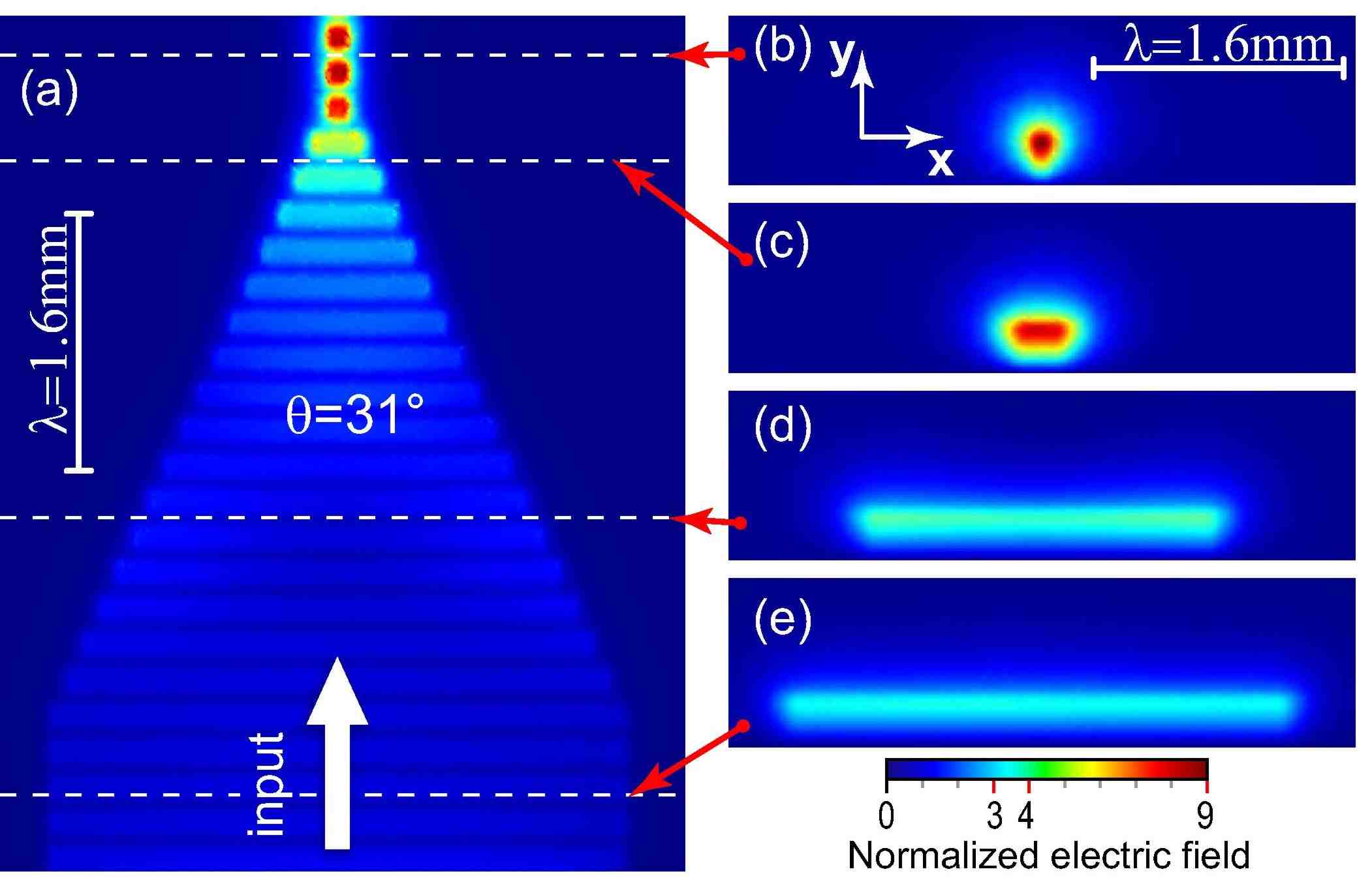
In the rest of the paper we present a number of devices enabling the spatial and temporal modulation of EM fields. The operating wavelength is and . In all ensuing computations the metal is considered as a PEC, to easily quantify the device radiation loss. Waveguide tapering maier06 ; rusina08 ; liang08 ; fernandez09b is interesting for field concentration and amplification, both important requirements for imaging applications kawata09 ; ishihara06 and circuit integration ishikawa09 . Tapering is expected to be easy in domino structures due to the insensitivity to lateral width of the dispersion relation of DPs. This hypothesis is confirmed in Fig. 3(a), which shows a top view of the propagation of power along a tapered domino structure. The lateral widths of the waveguide are at the input port (bottom) and at the output port (top). The length of the taper is , i.e., two wavelengths at the operating frequency, corresponding to a taper semi-angle of . Remarkably, reflection is smaller than 2% and only 5% of the incoming power is lost as radiation due to the shrinkage of the lateral dimension along the taper. Panels (b)-(e) are cross sections at different positions along the taper, vividly showing the process of field subwavelength concentration and enhancement. As mentioned above, the same design does not work in the telecom regime due to the sensitivity of DP bands to the lateral dimension at those frequencies. A more adiabatic taper, i.e., with smaller change of per unit length, would not circumvent the problem because absorption loss is high in the telecom regime (for instance, for , , and , the propagation length is ).
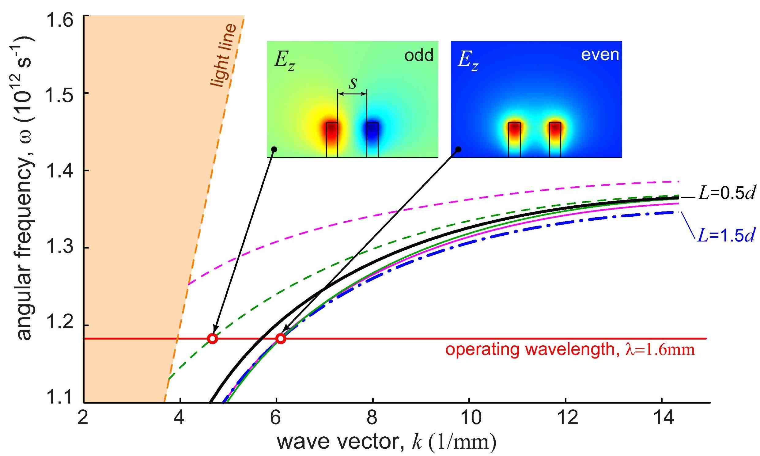
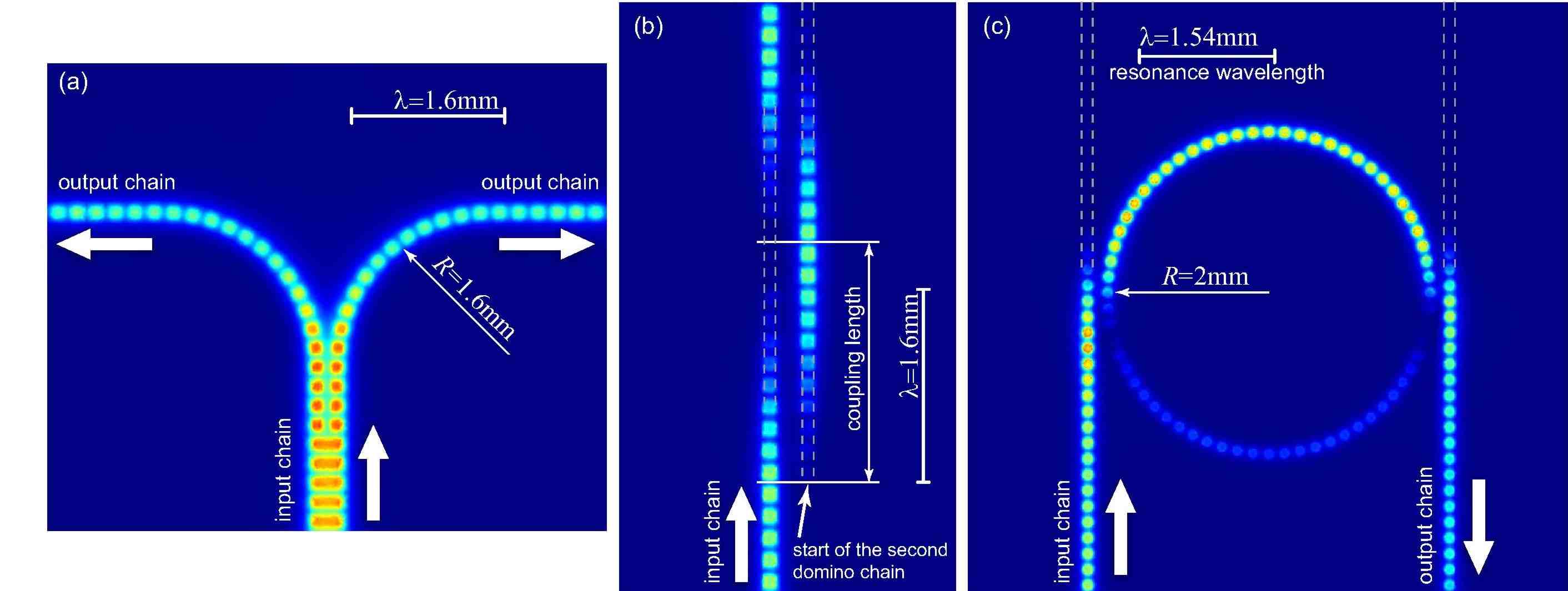
We now discuss how to construct power dividers and directional couplers huang08 ; nesterov08 . Figure 4 plots the dispersion relation of the modes supported by one and two parallel domino chains. Black solid line corresponds to the DP of . For two parallel waveguides (both with ), interaction gives rise to symmetric and antisymmetric supermodes which, for a separation , are shown by magenta curves with the solid line depicting the even supermode whereas the dashed one represents the odd supermode. Blue dashed-dotted line corresponds to a wider structure of and, importantly, this band stays very close to that of the even supermode. Due to this good overlapping, a simple linking of a wide domino structure with to two parallel domino chains (widths and separation ) should not result in an important impedance mismatch. This is verified in Fig. 5(a), displaying a top view of a power divider based on the previous idea. The input port () at the bottom feeds the wide domino which, after 5 periods, is linked to two parallel domino structures (, ). Due to symmetry only the even supermode is excited. The lateral separation between the individual waveguides is then increased, followed by waveguide bends. Simulations show that reflection is also negligible in this power splitter. Total radiation loss in the device is equal to that happening in the bends (previously discussed in Fig. 2(b)), each being 5% of the incoming power, which is small taking into account that the bend radius is equal to the operating wavelength.
Coupling between parallel domino structures can also be easily understood with the help of Fig. 4, displaying with green lines the even (solid) and odd (dashed) supermodes for parallel domino chains separated a distance . The insets show the modal shape of both modes. A larger is chosen in this simulation to prevent the cut-off of the odd supermode. The coupling length needed to exchange the carried power between the waveguides is estimated as . This value agrees with the result found in the simulation of a directional coupler. Figure 5(b) displays a top view of two parallel domino chains () separated a distance . A mode is launched in the left bottom waveguide and characteristic beatings with the predicted coupling length are observed when a second waveguide is located close to it.
As a final example a waveguide ring resonator is demonstrated, able to route various frequencies to different output ports bozhevolnyi06 . To show once more the robustness of our proposal, this device has been designed with posts of circular cross section as seen from above (radius ), instead of square cross section parallelepipeds. We have checked that similar results are obtained for the square geometry. The top view of this device is displayed in Fig. 5(c). For the chosen geometric parameters (ring radius , minimum separation in the coupling sections ), it is possible to drop a resonant wavelength at the output port. Non-negligible radiation losses only occur at the bends in the waveguide ring and they are about 25% of the input power, reasonably small considering that no optimization was attempted.
In summary, we have presented a new class of surface electromagnetic modes, termed domino plasmons, which feature an extraordinary characteristic: their insensibility to the lateral dimension of the structure supporting them. We have shown how the guiding properties of these modes enable the planar routing of THz radiation at a deep subwavelength level. Finally, the flexibility and versatility of waveguides based on domino plasmons have been demonstrated through the implementation of a variety of functional devices, which may thus prove very useful as a new concept for subwavelength THz circuitry.
III Methods
All results in this paper have been obtained by means of numerical simulations performed with the Finite Element Method (FEM) using commercial (COMSOL Multiphysics) software. A summary of the main modelling details follows. The technique is a volume FEM operating in frequency domain. Due to the various length scales involved, highly non-uniform meshes are used. In order to ensure an adequate representation of the electromagnetic fields, the size of the elements is a fraction of the skin depth inside the metallic parallelepipeds, a fraction of the characteristic geometric dimension (e.g., ) in the neighborhood of the structure, and a fraction of the operating wavelength at the boundaries of the simulation domain. The mesh size is refined until the results are stable with an accuracy of 1%. For instance, in the case of band structure computations, the convergence criterium is based on the value of both the real and imaginary parts of the wave vector. The final mesh is different for each simulation, but typical values of the tetrahedra sizes in different regions of the simulation domain are of the order of 1/5 of the skin depth and characteristic geometric dimension, and 1/10 of the wavelength. The typical number of degrees of freedom lies between and , a range in which the matrix equations are inverted with direct solvers. For the computation of band structures, the corresponding eigenvalue problem is posed in a single unit cell where Bloch boundary conditions together with Scattering boundary conditions are used. For device modelling, the excitation of the corresponding scattering problem is provided by Port boundary conditions, the ports being fed by the solutions of the corresponding eigenvalue problem. Open space is mimicked with Perfectly Matched Layers or/and Scattering boundary conditions. For the simulation of ideal metals, Perfect Electric Conductor (PEC) boundary conditions are employed. For realistic metals the dielectric permittivities are taken from Ref. [ordal83, ] for Al ( at ), and Ref. [johnson72, ] for Au ( at ). At low frequencies it was often sufficient to simulate the domains outside the conductors together with Surface Impedance Boundary Conditions, as verified by comparison with simulations fully accounting for the EM fields inside the metals.
References
- (1) Ferguson, B. and Zhang, X.-C. Materials for terahertz science and technology. Nature Mater. 1, 26-33 (2002).
- (2) Siegel, P. H. Terahertz technology. IEEE Trans. Microwave Theory and Tech. 50, 910-928 (2002).
- (3) Tonouchi, M. Cutting-edge terahertz technology. Nature Photon. 1, 97-105 (2007).
- (4) Withington, S. Terahertz astronomical telescopes and instrumentation. Phil. Trans. R. Soc. Lond. A 362, 395-402 (2004).
- (5) Siegel, P. H. Terahertz technology in Biology and Medicine. IEEE Trans. Microwave Theory and Tech. 52, 2438-2447 (2004).
- (6) Federici, J. F., Schulkin, B., Huang, F., Gary, D., Barat, R., Oliveira, F., and Zimdars, D. THz imaging and sensing for security applications - explosives, weapons and drugs. Semicond. Sci. and Technol. 20, 266-280 (2005).
- (7) Zhang, J. and Grischkowsky, D. Waveguide terahertz time-domain spectroscopy of nanometer water layers. Opt. Lett. 29, 1617-1619 (2004).
- (8) Cunningham, J., Byrne, M., Upadhya, P., Lachab, M., Linfield, E. H., and Davies, A. G. Terahertz evanescent field microscopy of dielectric materials using on-chip waveguides. Appl. Phys. Lett. 92, 032903 (2008).
- (9) Jamison, S. P., McGowan, R. W., and Grischkowsky, D. Single-mode waveguide propagation and reshaping of sub-ps terahertz pulses in sapphire fiber. Appl. Phys. Lett. 76, 1987-1989 (2000).
- (10) Han, H., Park, H., Cho, M., and Kim, J. Terahertz pulse propagation in a plastic photonic crystal fiber. Appl. Phys. Lett. 80, 2634-2636 (2002).
- (11) Nagel, M., Marchewka, A., and Kurz, H. Low-index discontinuity terahertz waveguides. Opt. Express 14, 9944-9954 (2006).
- (12) Jeon, T.-I. and Grischkowsky, D. THz Zenneck surface wave (THz surface plasmon) propagation on a metal sheet. Appl. Phys. Lett. 88, 061113 (2006).
- (13) Wang, K. and Mittleman, D. M. Metal wires for terahertz wave guiding. Nature 432, 376-379 (2004).
- (14) Pendry, J. B., Martin-Moreno, L., and Garcia-Vidal, F. J. Mimicking Surface Plasmons with Structured Surfaces. Science 305, 847-848 (2004).
- (15) Zhu, W., Agrawal, A., and Nahata, A. Planar plasmonic terahertz guided-wave devices. Opt. Express 16, 6216-6226 (2008).
- (16) Maier, S., Andrews, S. R., Martin-Moreno, L., and Garcia-Vidal, F. J. Terahertz Surface Plasmon-Polariton Propagation and Focusing on Periodically Corrugated Metal Wires. Phys. Rev. Lett. 97, 176805 (2006).
- (17) Fernandez-Dominguez, A. I., Moreno, E., Martin-Moreno, L., and Garcia-Vidal, F. J. Guiding terahertz waves along subwavelength channels. Phys. Rev. B 79, 233104 (2009).
- (18) Fernandez-Dominguez, A. I., Moreno, E., Martin-Moreno, L., and Garcia-Vidal, F. J. Terahertz wedge plasmon polaritons. Opt. Lett. 34, 2063-2065 (2009).
- (19) Garcia-Vidal, F. J., Martin-Moreno, L., and Pendry, J. B. Surfaces with holes in them: new plasmonic metamaterials. J. Opt. A: Pure Appl. Opt. 7, S97-S101 (2005).
- (20) Verhagen, E., Spasenovic, M., Polman, A., and Kuipers, L. K. Nanowire Plasmon Excitation by Adiabatic Mode Transformation. Phys. Rev. Lett. 102, 203904 (2009).
- (21) Berini, P. Plasmon-polariton waves guided by thin lossy metal films of finite width: Bound modes of symmetric structures. Phys. Rev. B 61, 10484 (2000).
- (22) Sengupta, D. L. On the phase velocity of wave propagation along an infinite Yagi structure. IRE Trans. Antennas Propag. 7, 234-239 (1959).
- (23) Krenn, J. R., Dereux, A., Weeber, J. C., Bourillot, E., Lacroute, Y., Goudonnet, J. P., Schider, G., Gotschy, W., Leitner, A., Aussenegg, F. R., and Girard, C. Squeezing the Optical Near-Field Zone by Plasmon Coupling of Metallic Nanoparticles. Phys. Rev. Lett. 82, 2590-2593 (1999).
- (24) Maier, S. A., Brongersma, M. L., and Atwater, H. A. Electromagnetic energy transport along arrays of closely spaced metal rods as an analogue to plasmonic devices. Appl. Phys. Lett. 78, 16-18 (2001).
- (25) Rusina, A., Durach, M., Nelson, K. A., and Stockman, M. I. Nanoconcentration of terahertz radiation in plasmonic waveguides. Opt. Express 16, 18576-18589 (2008).
- (26) Liang, H., Ruan, S., and Zhang, M. Terahertz surface wave propagation and focusing on conical metal wires. Opt. Express 16, 18241-18248 (2008).
- (27) Kawata, S., Inouye, Y., and Verma, P. Plasmonics for near-field nano-imaging and superlensing. Nature Photon. 3, 388-394 (2009).
- (28) Ishihara, K., Ohashi, K., Ikari, T., Minamide, H., and Yokoyama, H. Terahertz-wave near-field imaging with subwavelength resolution using surface-wave-assisted bow-tie aperture. Appl. Phys. Lett. 89, 201120 (2006).
- (29) Ishikawa, A., Zhang, S., Genov, D. A., Bartal, G., and Zhang, X. Deep Subwavelength Terahertz Waveguides Using Gap Magnetic Plasmon. Phys. Rev. Lett. 102, 043904 (2009).
- (30) Huang, W., Zhang, Y., and Li, B. Ultracompact wavelength and polarization splitters in periodic dielectric waveguides. Opt. Express 16, 1600-1609 (2008).
- (31) Nesterov, M. L., Kats, A. V., and Turitsyn, S. K. Extremely short-length surface plasmon resonance devices. Opt. Express 16, 20227-20240 (2008).
- (32) Bozhevolnyi, S. I., Volkov, V. S., Devaux, E., Laluet, J.-Y., and Ebbesen, T. W. Channel plasmon subwavelength waveguide components including interferometers and ring resonators. Nature 440, 508-511 (2006).
- (33) Ordal, M. A., Long, L. L., Bell, R. J., Bell, S. E., Bell, R. R., Alexander, R. W., and Ward, C. A. Optical properties of the metals Al, Co, Cu, Au, Fe, Pb, Ni, Pd, Pt, Ag, Ti, and W in the infrared and far infrared. Appl. Opt. 22, 1099-1119 (1983).
- (34) Johnson, P. and Christy, R. Optical constants of the nobel metals. Phys. Rev. B 6, 4370-4379 (1972).