Interlayer screening effect in graphene multilayers with ABA and ABC stacking
Abstract
We study the effect of perpendicular electric fields on the band structures of ABA and ABC graphene multilayers, and find that the electronic screening effect is significantly different between them. In ABA multilayers, the field produces a band overlap and gives a linear screening, while in ABC multilayers, in contrast, it opens an energy gap in the surface-state band at low energy, leading to a strong screening effect essentially non-linear to the field amplitude. The energy gap of a large ABC stack sharply rises when the external field exceeds a certain critical value.
I Introduction
Recent experimental realizations of atomically-thin graphene systems novo04 ; novo05 ; zhang05 open up possibilities of exploring their exotic electronic properties. In multilayer films composed of more than two graphene layers, the interlayer coupling strongly modifies the linear dispersion of monolayer graphene, resulting in various electronic structures depending on the number of layers, . novo06 ; Ohta06 ; Ohta07 ; McCa06 ; Koshino_and_Ando_2006a ; Nils06 ; Guin06 ; Lati06 ; Lu06 ; Part06 ; Koshino_and_Ando_2007b ; manes07 ; Koshino_and_Ando_2008a ; kosh09_ssc ; kosh09_aba ; avet09 ; guett08 ; crac09 ; avet09b The band structure can also be changed by applying a gate electric field perpendicular to the layer, through generating an interlayer potential asymmetry. In bilayer graphene, for example, an energy gap opens between the conduction and valence bands in presence of gate electric field McCa06 ; Lu06 ; Guin06 ; mcc06b ; mcc07 ; min07 ; aoki07 ; gava09 ; avet09b and it was actually observed in transport castro07 ; oost08 and spectroscopic measurements Ohta06 ; Ohta07 ; li09 ; zhang08 ; kuzmenko ; zhang09 ; mak09 .
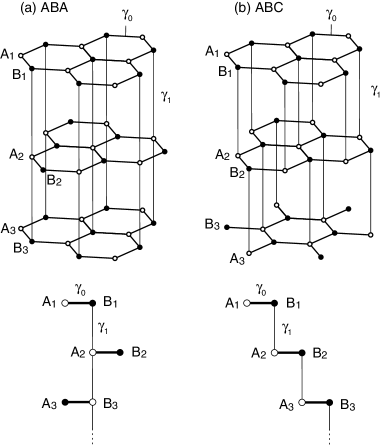
In nature, there are two known forms of bulk graphite called ABA (AB, hexagonal, or Bernal) and ABC (rhombohedral) with different stacking manners as shown in Fig. 1. The ABA phase is thermodynamically stable and common, while it is known that some portion of natural graphite takes the ABC form. lipson42 For ABA graphite, the effective mass model describing the electronic property was developed for the bulk system Wall47 ; Slon58 ; McCl56 ; McCl57 ; McCl60 ; Dres65 ; dressel02 , and also for few-layer systems. McCa06 ; Koshino_and_Ando_2006a ; Nils06 ; Guin06 ; Lu06 ; Part06 ; Koshino_and_Ando_2008a ; kosh09_ssc ; Koshino_and_Ando_2007b ; manes07 ; kosh09_aba . The energy dispersion of the multilayer graphenes includes the subbands analog to monolayer or the bilayer graphene, Guin06 ; Part06 and the Hamiltonian is actually decomposed into independent subsystems effectively identical to monolayer or bilayer. Koshino_and_Ando_2007b ; Koshino_and_Ando_2008a The ABC graphite has a quite different electronic structure from ABA’s haering58 ; mcclure69 ; Guin06 ; lu06abc ; Lati06 ; aoki07 ; lu07abc ; min08 ; arovas08 ; kosh09_abc . In particular, the low-energy band of a finite ABC multilayer are given by the surface states localized at outer-most layers, Guin06 ; manes07 and the interlayer potential asymmetry opens an energy gap in those bands. aoki07 ; lu07abc ; kosh09_abc This is in sharp contrast with ABA multilayers where potential asymmetry causes a band overlapping. aoki07 ; kosh09_aba
In considering the interlayer potential asymmetry induced by an external electric field, it is essential to take into account screening effect, as done in bilayer graphene,mcc06b ; mcc07 ; min07 and ABA multilayers guin_scr ; kosh09_aba ; avet09b . Experimentally, the interlayer screening effect in the gate electric field was probed in thin graphite films. Ohta07 ; Miya08 ; Lee09 ; Sui09 Here we calculate the self-consistent band structure of ABA and ABC multilayers with various ’s in the presence of perpendicular electric field. For ABA multilayers, we show that the electric field generally produces band overlapping, and the screening is shown to be linear to the field amplitude. In ABC multilayers, on the other hand, the low-energy surface band causes a strong non-linear screening effect through opening an energy gap. The paper is organized as follows: we present the effective mass models for ABA and ABC multilayers in Sec. II, and compute the band structure including the self-consistent screening effect in Sec. III. The conclusion is given in Sec. IV
II Effective Hamiltonian and band structure
II.1 ABA multilayers
We first consider a multilayer graphene with ABA stacking, composed of layers of a graphene layers. We label and on -th layer as and . In ABA stacking, the sites are arranged along vertical columns normal to the layer plane, while the rest sites are above or below the center of hexagons in the neighboring layers, as shown in Fig. 1 (a). The system is described by a kp Hamiltonian based on three-dimensional (3D) graphite model. Wall47 ; Slon58 ; McCl56 ; McCl57 ; McCl60 ; Dres65 ; dressel02 As the simplest approximation, we include parameter describing the nearest neighbor coupling within each layer, and for the coupling of the interlayer vertical bonds. The band parameters were experimentally estimated in the bulk ABA graphite, for example dressel02 as eV and eV, which we will use in the following calculations. The lattice constant of honeycomb lattice (distance between nearest atoms) is given by nm, and the inter-layer spacing nm.
The low-energy spectrum is given by the states in the vicinity of and points in the Brillouin zone. Let and be the Bloch functions at the point, corresponding to the and sublattices, respectively, of layer . If the basis is taken as ; ; ; , the Hamiltonian around the point is given by Guin06 ; Part06 ; Lu06 ; Koshino_and_Ando_2007b
| (1) |
and
| (2) |
where is the electrostatic potential at th layer, and we defined with . is the band velocity of monolayer graphene given by . The effective Hamiltonian for another valley, , is obtained by interchanging and . McCa06
When , Hamiltonian (1) can be decomposed into subsystems identical to bilayer or monolayer graphenes with a basis appropriately chosen. Koshino_and_Ando_2007b The subsystems are labeled by an index which ranges as
| (5) |
The eigenenergies at are given Guin06 ; Koshino_and_Ando_2007b for as , and for as
| (6) |
where , , , and
| (7) |
only exists in odd-layer graphene and gives an energy band identical to monolayer graphene. Other ’s are bilayer-type band structures where gives a pair of electron () and hole bands () touching at zero energy, and another pair repelled away by . The dispersion around is approximately quadratic with the effective mass McCa06
| (8) |
giving the density of states at zero energy, , with and are valley () and spin degeneracies, respectively.
The quantity corresponds to the wave number in the layer stacking direction (-direction) via . Guin06 ; Koshino_and_Ando_2007b The wave function of subband is indeed a standing wave in -direction with wave number . The total density of states per layer, , approximates in large limit,
| (9) |
where is replaced with integration in .
II.2 ABC multilayers
The ABC multilayer have a different arrangement shown in Fig. 1 (b), where vertical bonds couple the pairs for . We use the same notation and as in ABA graphite, for the nearest intralayer and interlayer coupling, respectively. Although the band parameters are not identical between ABA and ABC graphites, we refer to the values of ABA in the following numerical calculations, assuming that the corresponding coupling parameters have similar values. mcclure69 Hamiltonian around the point can be written as mcclure69 ; Guin06 ; lu06abc ; arovas08
| (10) |
with the same matrices defined in Eq. (2). When =0, the eigenenergies are given by
| (11) |
with and being solutions of
| (12) |
The corresponding wavefunction is with
| (13) |
where and is a normalization factor. In the bulk limit, corresponds to the wavenumber along the layer stacking () direction. Actually, Eq. (12) is obtained by imposing a condition that a standing wave in -direction, composed by bulk wavefunctions, becomes zero at fictitious sites and out of the system.
Equation (12) has solutions of giving independent eigenstates. All of are real when , while only one becomes complex when , which corresponds to the evanescent mode in the bulk. In , the complex branch approximates , giving the dispersion
| (14) |
with . These are the only bands which appear at and dominate the low-energy physics. The corresponding wavefunction is
| (15) |
The wave amplitude becomes largest on the top and bottom layers and decays exponentially inside, and thus is regarded as a surface state Guin06 . The wave function is exactly localized at the sites and at , and as increases, the decay length increases as in units of interlayer spacing . In Fig. 4, we plot the band structures of ABC graphenes with and 20, where the results of are indicated as black dotted curves. The surface states of Eq. (14) are shown as a pair of electron and hole bands touching at , which become flatter as increases. The bilayer graphene (AB) can be regarded as of ABA family and also that of ABC family, and indeed, equally described either of Eqs. (6) or (11).
When we consider the low-energy physics around zero energy, it is convenient to use the effective Hamiltonian reduced to the basis . McCa06 ; manes07 ; min08 In presence of , it reads
| (16) |
This approximation is valid when , i.e., the actual wave function, Eq. (15), is well localized to or . When we set the origin of potential as , the eigenenergy is given by
| (17) |
where and . The potential difference opens an energy gap between the valence and conduction bands.
III Screening effects
III.1 Self-consistent treatment of screening effect
We compute the band structure of ABA or ABC multilayer graphenes in presence of gate electric field taking account of the screening effect. We consider undoped free-standing multilayer graphenes with an external electric field applied to the perpendicular direction. This situation can be realized in an experimental set up with an external top and bottom gates electrodes which are held at the opposite gate voltages with respect to the graphene. kosh09_aba
The potential at each layer, should be determined self-consistently. If a set of is given, we can compute the band structure using the Hamiltonian Eq. (1) for ABA or Eq. (10) for ABC multilayers. Then we determine the Fermi energy so that the total density is equal to ( in the present case), and calculate the electron density at each layer, , from the occupied eigenstates. For screening effect, we consider the multilayer as parallel plates with zero thickness and respective electron densities . The electric field between th and th layers is then given by
| (18) |
Here is the permittivity of the interlayer spaces without the screening effect of -band electrons, and we set in the following calculations. Eq. (18) immediately gives a new set of the electrostatic potential , which should be identical to the initial . To find the self-consistent solution, we employ an iterative numerical approach, where we start with as initial values and iterate the process until ’s converge.
III.2 ABA multilayers
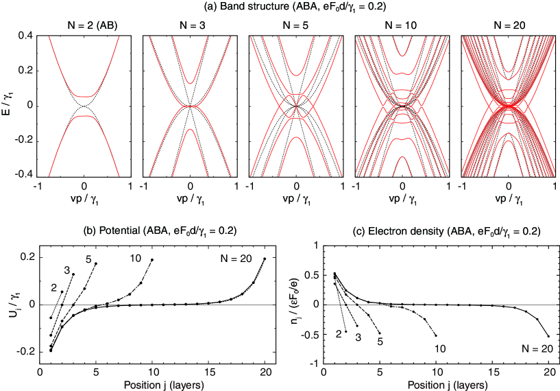
In Fig. 2 (a), solid red curves show the self-consistent band structures of ABA multilayers with several ’s, in presence of the external field . The original band structures at are also shown as dotted black curves. In , we see that the lowest electron band is pulled down and the highest hole band is lifted up, making a band overlap around zero energy, as was previously recognized in the case of and 4. aoki07 ; kosh09_aba The energy width of overlap becomes almost constant in .
Figures 2(b) and 2(c) show the corresponding potential distribution and electron density , respectively, at the same external field . In , we observe that the electric field (i.e., gradient in ) is screened within a few layers from the surface, leaving a triangular potential pocket at each end. The potential decay near the edge is almost identical between and 20. The overlapping bands observed in Fig. 2 (a) are actually the bound states trapped at either of pockets; the states of the lowest electron and the highest hole bands are indeed localized at the potential minimum (left end) and maximum (right), respectively. Since is zero, those bands are populated by electrons or holes, contributing to the most part of the screening field. A smooth decay observed in the electron density appears different from Ref. guin_scr , which finds a charge oscillation with every second layer. We presume that this is due to the contribution from the intraband excitation, which was dropped in numerical calculations for neutral systems in Ref. guin_scr .
The typical screening length (penetrating depth of electric field) can be roughly estimated by Thomas-Fermi approximation. guin_scr In this treatment, the potential decay on the surface is expressed as with , where is the three dimensional density of states at the Fermi energy. For graphene, if we substitute with of Eq. (9), we obtain guin_scr
| (19) |
Using the parameters above, we get nm. In Fig. 2 (b), we plot an exponential curve with decay length in Eq. (19) as a dotted curve to fit with the right half of the curve of , which shows a fairly nice agreement. The depth of potential depth, or , is roughly estimated as , which determines the order of the energy width in band overlapping.
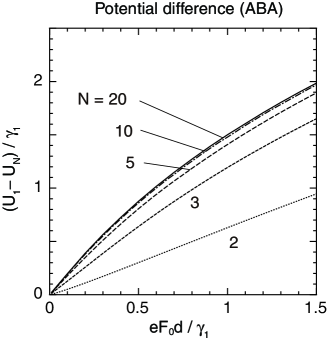
Figure 3 displays the potential difference as a function of the external field . rises almost linearly in increasing , except for a slight sub-linear components in large . This is consistent with Thomas-Fermi approximation, since it gives linear screening in a weak external field.
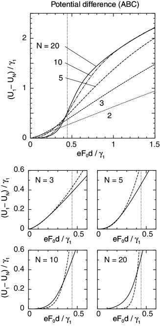
III.3 ABC multilayers
The screening property of ABC multilayers is quite different from that of ABA, as the density of states diverges at due to the flat band of the surface states. Before numerical calculations with full band model, we present an analytical approach using the effective Hamiltonian of Eq. (16) valid in low energies. The potential difference between the top and bottom layers opens an energy gap between the valence and conduction bands, and thus only the lower band is occupied when . The density difference between the top and bottom layers, , is calculated as
| (20) | |||||
where is the eigenvector of Eq. (16) for band, and
| (21) |
with is the gamma function.
The density imbalance causes the screening field opposed to the external field , resulting in the total potential difference . Together with Eq. (20), we obtain the self-consistent equation for ,
| (22) |
In , is negligible compared to when is small enough. Then the equation is solved approximately as
| (23) |
which is essentially non-linear in . In large- limit, we have and thus , where is a characteristic field with an associated electron density
| (24) |
In increasing , rapidly increases when the external field exceeds .
is the electron density accommodated in the flat-band region in large limit (), i.e., the number of surface states. The field is completely screened in , because the surface states are able to supply positive and negative charge to opposite surfaces to cancel the external field. The screening collapses at , when the density required for canceling exceeds the surface states population .
(AB) is an exceptional in that the integration in Eq. (21) diverges logarithmically, giving infinite . Actually this is an artifact of the reduced model, due to the incorrect contributions from large where the reduced Hamiltonian is not accurate. We can remove this by introducing a momentum cut-off , and get . When we neglect the logarithmic dependence of , becomes linear in in accordance with Eq. (22). The logarithmic factor gives a weak singularity at .
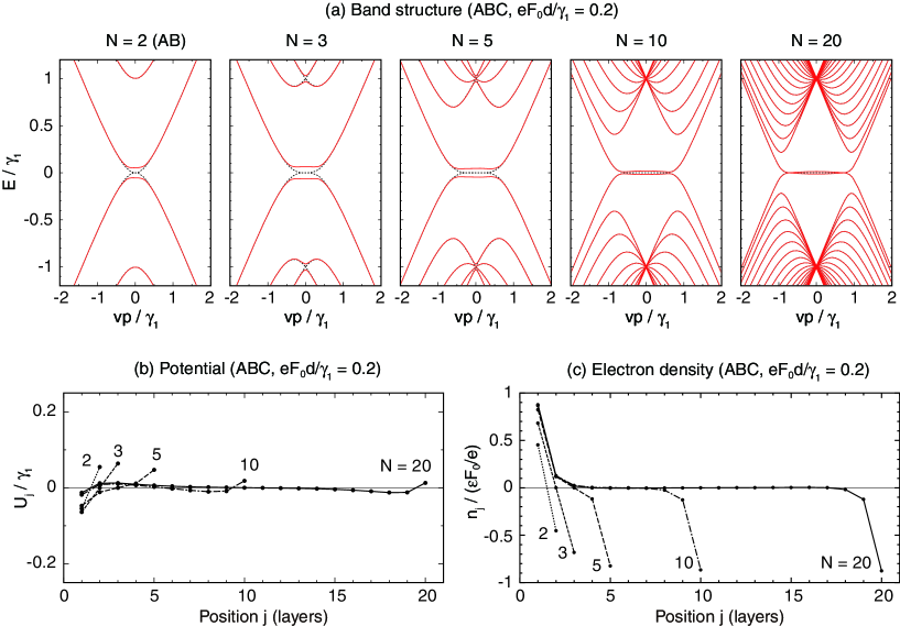
Now we numerically calculate the self-consistent band structure of ABC multilayers using the full Hamiltonian Eq. (10). Figure 4 (a) shows the results at (red, solid) and 0 (black, dotted). In presence of the external field, an energy gap opens at low-energy as expected. The gap width becomes smaller in in increasing , suggesting a strong screening effect in large stacks. Figures 4(b) and 4(c) show the corresponding potential distribution and the electron density , respectively, at the same field . At , the potential is almost flat inside, as the external field is mostly screened by the electric charge on surface states localized at the outermost layers. This is in contrast with ABA multilayers, where an external field always penetrates inside with a few-layer thickness.
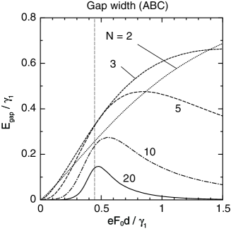
Figure 5 shows the plots of the potential difference as a function of the external field . We actually observe non-linear behavior expected in the analytical argument, where rapidly increases at (shown as a dashed vertical line). Lower panels in Fig. 5 compare the numerical results (solid) to the analytical expression Eq. (23) (dashed). We have nice agreements for in small , while the approximation becomes worse in large stack of . In large ’s, the low-energy band almost reaches , where the wave function deeply penetrates into the bulk in accordance with Eq. (15). The finite penetration length makes the screening less effective, compared to the previous model assuming the wave functions perfectly localized on the surface layers. As a result, numerical curves at large ’s rise less sharply than the analytical ones as observed in Fig. 5. The wave penetration to the bulk is also responsible for Mexican hat structure, Guin06 or narrowing of the gap around observed in Fig. 4 (a). There the actual energy splitting becomes smaller than because the wave function is not perfectly localized at surface layers.
The width of the energy gap is an important quantity which can be detected experimentally. Figure 6 shows the gap width against the external field in the self-consistent band structures of ABC multilayers. In , the band bottom is approximately flat and the gap width therefore approximates (the splitting at ), and actually rises in proportional to . In large stacks of , the energy gap becomes maximum around , and is suppressed in greater ’s, due to the gap narrowing at .
IV Conclusion
We studied electronic band structures of ABA and ABC graphene multilayers in the presence of an perpendicular electric field, including the screening effect. In ABA multilayers, the electric field produces band overlapping accompanying a linear screening well described by the Thomas-Fermi approximation. In ABC multilayers, in contrast, the surface state bands dominating low energies cause a strong non-linear screening effect through opening an energy gap.
While in the present model we only include the primary parameters and in our model, the extra band parameters corresponding to the further hopping generally affect the band structure of multilayer graphenes. Wall47 ; Slon58 ; McCl57 ; McCl60 ; Dres65 ; dressel02 In ABC graphenes, it was shown that the extra parameters gives a fine structure to the surface band, of which energy scale is expected to be of the order of 10 meV. kosh09_abc We expect that the screening property would be influenced by those effects when the external potential is as small as those energy scales. As another remark, the electron-electron interaction other than the screening effect may create non-trivial ground states in a flat band such as in ABC multilayers, while we leave those problems for future works.
Acknowledgments
The author thanks E. McCann and T. Ando for helpful discussions. This work was supported in part by Grant-in-Aid for Scientific Research on Priority Area “Carbon Nanotube Nanoelectronics” and by Grant-in-Aid for Scientific Research from Ministry of Education, Culture, Sports, Science and Technology Japan.
References
- (1) K. S. Novoselov, A. K. Geim, S. V. Morozov, D. Jiang, Y. Zhang, S. V. Dubonos, I. V. Grigorieva, A. A. Firsov, Science 306, 666 (2004).
- (2) K. S. Novoselov, A. K. Geim, S. V. Morozov, D. Jiang, M. I. Katsnelson, I. V. Grigorieva, S. V. Dubonos, and A. A. Firsov, Nature 438, 197 (2005).
- (3) Y. Zhang, Y.-W. Tan, H. L. Stormer, and P. Kim, Nature 438, 201 (2005).
- (4) K. S. Novoselov, E. McCann, S. V. Morozov, V. I. Fal ko, M. I. Katsnelson, U. Zeitler, D. Jiang, F. Schedin, and A. K. Geim, Nat. Phys. 2, 177 (2006).
- (5) T. Ohta, A. Bostwick, T. Seyller, K. Horn, and E. Rotenberg, Science 313 (2006) 951.
- (6) T. Ohta, A. Bostwick, J. L. McChesney, T. Seyller, K. Horn, and E. Rotenberg, Phys. Rev. Lett. 98, 206802 (2007).
- (7) E. McCann and V. I. Fal’ko, Phys. Rev. Lett. 96, 086805 (2006).
- (8) M. Koshino and T. Ando, Phys. Rev. B 73, 245403 (2006).
- (9) J. Nilsson, A. H. Castro Neto, F. Guinea, and N. M. R. Peres, Phys. Rev. Lett. 97, 266801 (2006).
- (10) F. Guinea, A. H. Castro Neto, and N. M. R. Peres, Phys. Rev. B 73, 245426 (2006).
- (11) S. Latil and L. Henrard, Phys. Rev. Lett. 97, 036803 (2006).
- (12) C. L. Lu, C. P. Chang, Y. C. Huang, J. M. Lu, C. C. Hwang, and M. F. Lin, J. Phys. Condens. Matter 18, 5849 (2006); C. L. Lu, C. P. Chang, Y. C. Huang, R. B. Chen, and M. L. Lin, Phys. Rev. B 73, 144427 (2006).
- (13) B. Partoens and F. M. Peeters, Phys. Rev. B 74, 075404 (2006); ibid. 75, 193402 (2007).
- (14) M. Koshino and T. Ando, Phys. Rev. B 76, 085425 (2007).
- (15) J. L. Mañes, F. Guinea, and M. A. H. Vozmediano, Phys. Rev. B 75, 155424 (2007).
- (16) M. Koshino and T. Ando, Phys. Rev. B 77, 115313 (2008).
- (17) M. Koshino and T. Ando, Solid State Commun. 149, 1123 (2009).
- (18) M. Koshino and E. McCann, Phys. Rev. B 79 125443 (2009).
- (19) A. A. Avetisyan, B. Partoens and F. M. Peeters, Phys. Rev. B 79, 035421 (2009).
- (20) A. A. Avetisyan, B. Partoens and F. M. Peeters, Phys. Rev. B 80, 195401 (2009).
- (21) J. Güttinger, C. Stampfer, F. Molitor, D. Graf, T. Ihn, and K. Ensslin, New J. Phys. 10, 125029 (2008).
- (22) M. F. Craciun, S. Russo, M. Yamamoto, J. B. Oostinga, A. F. Morpurgo, and S. Tarucha, Nat. Nanotechnol. 4, 383 (2009).
- (23) E. McCann, Phys. Rev. B 74, 161403(R) (2006).
- (24) E. McCann, D. S. L. Abergel and V. I. Fal’ko, Solid State Commun. 143, 110 (2007).
- (25) H. Min, B. R. Sahu, S. K. Banerjee, and A. H. MacDonald, Phys. Rev. B 75, 155115 (2007).
- (26) M. Aoki and H. Amawashi, Solid State Commun. 142 123 (2007).
- (27) P. Gava, M. Lazzeri, A. M. Saitta and F. Mauri, Phys. Rev. B 79, 165431 (2009).
- (28) E. V. Castro, K. S. Novoselov, S. V. Morozov, N. M. R. Peres, J. M. B. Lopes dos Santos, J. Nilsson, F. Guinea, A. K. Geim, and A. H. Castro Neto, Phys. Rev. Lett. 99, 216802 (2007).
- (29) J. B. Oostinga, H. B. Heersche, X. Liu, A. F. Morpurgo, and L. M. K. Vandersypen, Nature Mater. 7, 151 (2008).
- (30) Z. Q. Li, E. A. Henriksen, Z. Jiang, Z. Hao, M. C. Martin, P. Kim, H. L. Stormer, and D. N. Basov, Phys. Rev. Lett. 102, 037403 (2009).
- (31) L. M. Zhang, Z. Q. Li, D. N. Basov, M. M. Fogler, Z. Hao and M. C. Martin, Phys. Rev. B 78, 235408 (2008).
- (32) A. B. Kuzmenko, E. van Heumen, D. van der Marel, P. Lerch, P. Blake, K. S. Novoselov, and A. K. Geim, Phys. Rev. B 79, 115441 (2009).
- (33) Y. Zhang, T.-T. Tang, C. Girit, Z. Hao, M. C. Martin, A. Zettl, M. F. Crommie, Y. R. Shen, and F. Wang, Nature 459, 820 (2009).
- (34) K. F. Mak, C. H. Lui, J. Shan and T. F. Heinz, Phys. Rev. Lett. 102, 256405 (2009).
- (35) H. Lipson and A. R. Stokes, Proc. Roy. Soc., A181, 101 (1942).
- (36) P. R. Wallace, Phys. Rev. 71, 622 (1947)
- (37) J. W. McClure, Phys. Rev. 104, 666 (1956).
- (38) J. W. McClure, Phys. Rev. 108, 612 (1957).
- (39) J. C. Slonczewski and P. R. Weiss, Phys. Rev. 109, 272 (1958).
- (40) J. W. McClure, Phys. Rev. 119, 606 (1960).
- (41) G. Dresselhaus and M. S. Dresselhaus, Phys. Rev. 140, A401 (1965).
- (42) M. S. Dresselhaus and G. Dresselhaus, Adv. Phys. 51, 1 (2002).
- (43) R. R. Haering, Can. J. Phys. 36, 352 (1958).
- (44) J. W. McClure, Carbon 7, 425 (1969).
- (45) C. L. Lu, H. C. Lin, C. C. Hwang, J. Wang, M. F. Lin, and C. P. Chang, Appl. Phys. Lett. 89, 221910 (2006).
- (46) C. L. Lu, C. P. Chang, Y. C. Huang, J. H. Ho, C. C. Hwang, and M. F. Lin, J. Phys. Soc. Jpn. 76, 024701 (2007).
- (47) H. Min and A. H. MacDonald, Phys. Rev. B 77, 155416 (2008).
- (48) D. P. Arovas and F. Guinea, Phys. Rev. B 78, 245416 (2008).
- (49) M. Koshino and E. McCann, Phys. Rev. B 80, 165409 (2009).
- (50) F. Guinea, Phys. Rev. B 75, 235433 (2007).
- (51) H. Miyazaki, S. Odaka, T. Sato, S. Tanaka, H. Goto, A. Kanda, K. Tsukagoshi, Y. Ootuka, and Y. Aoyagi, Appl. Phys. Exp. 1, 034007 (2008).
- (52) N. J. Lee, J. W. Yoo, Y. J. Choi, C. J. Kang, D. Y. Jeon, D. C. Kim, S. Seo, and H. J. Chung, Appl. Phys. Lett. 95, 222107 (2009).
- (53) Y. Sui and J. Appenzeller, Nano Lett. 9, 2973 (2009).