E-mail: zrlpet@ch.ibm.com.
Nonlinear screening of charges induced in graphene by metal contacts
Abstract
To understand the band bending caused by metal contacts, we study the potential and charge density induced in graphene in response to contact with a metal strip. We find that the screening is weak by comparison with a normal metal as a consequence of the ultra-relativistic nature of the electron spectrum near the Fermi energy. The induced potential decays with the distance from the metal contact as and for undoped and doped graphene, respectively, breaking its spatial homogeneity. In the contact region the metal contact can give rise to the formation of a -, -, - junction (or with additional gating or impurity doping, even a -- junction) that contributes to the overall resistance of the graphene sample, destroying its electron-hole symmetry. Using the work functions of metal-covered graphene recently calculated by Khomyakov et al. [Phys. Rev. B 79, 195425 (2009)] we predict the boundary potential and junction type for different metal contacts.
pacs:
73.40.Ns, 81.05.ue, 73.40.Cg, 72.80.VpI Introduction
Graphene’s unique electronic properties arise from the ultra-relativistic character of the electron spectrum near the Fermi energy that leads to many unusual physical effects.Novoselov:nat05 ; Zhang:nat05 ; Katsnelson:natp06 ; Karpan:prl07 The high mobility and low electron density (compared to normal metals) of this two-dimensional form of carbon suggest various possibilities for using single and multiple graphene sheets to make electronic devices.Novoselov:nat05 ; Zhang:nat05 ; Katsnelson:natp06 ; Karpan:prl07 ; Giovannetti:prb07 ; Huard:prl07 ; Danneau:prl08 ; Lee:natn08 ; Gorbachev:nanol08 ; Rotenberg:natm08 For example, one can use external gates to locally change the doping of graphene and so design - or -- junctions.Huard:prl07 ; Cheianov:prb06 How charge inhomogeneities are then induced in graphene by the gate electrodes or by charged impurities has been studied theoretically in Refs. DiVincenzo:prb84, ; Katsnelson:prb06, ; Zhang:prl08, ; Fogler:prb08, .
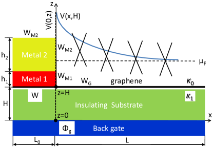
Recently, we have shown how a graphene sheet adsorbed on a metal is charged by the metalGiovannetti:prl08 ; Khomyakov:prb09 suggesting an alternative way of making - junctions by putting weakly-interacting metal strips on graphene. The (out-of-plane) charge transfer between graphene and the metal is determined by (i) the difference between the work function of graphene and the metal surface, and (ii) the metal-graphene chemical interaction that creates an interface dipole which lowers the metal work function. Depositing a metal strip (electrode) of finite width on the graphene sheet will additionally result in an in-plane charge transfer from the graphene region covered by the metal to the “free” graphene supported by a dielectric, driven by the difference between the work functions of the metal, , of metal-covered graphene, , and of free-standing graphene, . Khomyakov:prb09 An electrostatic potential will then be induced across the graphene sheet, leading to band bending and the formation of a -, - or - junction at the contact area as illustrated in Fig. 1.Huard:prb08 ; Lee:natn08
In this paper we study how graphene screens charges transferred from the metal-graphene contact to “free” graphene, creating an electrostatic potential barrier at the contact region, see Fig. 1. This problem is of fundamental importance since the physics of contacts can have a significant effect on the transport properties of an electronic device, in particular, graphene-based devices with “invasive” electrodes, as recently demonstrated in Ref. Huard:prb08, . A widely-used picture of a metal-graphene contact often assumes a quite sharp potential step at the contact.Tworzydlo:prl06 However, we find that the screening in graphene is strongly suppressed leading to a large-scale inhomogeneity of the electrostatic potential across the graphene sample. The contact effects can also result in charge inhomogeneities of different polarities (an abrupt - junction) at the contact region. These abrupt - junctions are qualitatively different from the gate-induced - junctions recently reported in Refs. Huard:prl07, ; Cheianov:prb06, ; Zhang:prl08, .
The contact phenomenon studied in the present work stems from long-range electric fields originating from charge transferred between a graphene sheet and a metal electrode. Recently, Barraza et al. have obtained a contact potential from density functional theory calculations of graphene ribbons with a length of nm contacted with aluminium electrodes.Barraza:prl10 To calculate the contact potential profile one applies periodic boundary conditions, i.e. periodic arrays of metal-graphene junctions. Using such results to describe a single metal-graphene junction, one assumes that the periodic images do not interact, or, in other words, that the contact potential profile is confined to a narrow region around the junction. Indeed the phenomenological model proposed in Ref. Barraza:prl10, suggests an exponential-like decay of the potential induced in graphene by a metal contact. Our results show that this does not apply to a single metal-graphene contact, where the induced potential is in fact long range.
In Sec. II we describe the Thomas-Fermi approach used to study the band banding caused by metal contacts in graphene. In Sec. III we derive the induced potential and charge density for undoped, doped and gated graphene, and make material-specific predictions of the boundary potential and junction type for different metal contacts. Our conclusions are presented in Sec. IV.
II Thomas-Fermi approach
We model a graphene-metal contact as shown in Fig. 1. Metal contacts are often applied as a bilayer; a (thin) layer of metal 1 takes care of a good adhesion to graphene, and a (thick) layer of metal 2 forms the electrode. We allow for electrostatic doping by means of a back gate electrode, and model chemical doping by a uniform background charge . The resulting screening potential in graphene is calculated using density functional theory (DFT) within the Thomas-Fermi (TF) approximation. The latter has proven to have a wide range of validity for describing screening in graphene.DiVincenzo:prb84 ; Katsnelson:prb06 ; Zhang:prl08 ; Fogler:prb08 In TF theory the charge density induced in graphene for is given in terms of the local chemical potential as , where (eV2 unit cell), Å2 is the unit cell area of graphene, and the elementary charge.Giovannetti:prl08 The electrostatic potential and the local chemical potential are related as with and the graphene sheet is located at , where is the distance between the graphene sheet and the backgate electrode, see Fig. 1. The chemical potential of the entire system, , is set to zero for undoped graphene.
Using the Poisson equation and translational symmetry in the direction, (i.e. assuming an infinitely wide graphene sample), the TF equation for the electrostatic potential induced in graphene () is
| (1) |
where with . The effects of the substrate, the lattice potential and of the filled band electrons are taken into account via an effective dielectric constant, , and a compensating charge .Katsnelson:prb06 ; Ando:jpsj06 The boundary conditions for are imposed by the potential at the contact and at the gate . Assuming graphene is a nearly perfect metal, i.e. , which will be justified below, the boundary conditions are given byPolyanin:02 ; Landau:84 ; Shikin:prb01
| (2) | |||||
| (3) | |||||
where and is the angle between the “free” graphene sheet and face of the metal electrode; , , and are the work functions of the bottom and top metal layers, graphene and graphene-covered metal, respectively. is the backgate voltage.
Using a Green function approach, Eq. (1) can be formulated as a nonlinear integral equationPolyanin:02
| (4) | |||||
| (5) | |||||
Using Eqs. (2) and (3) the boundary potential term can be written as
| (6) | |||||
where the boundary potential constants and are
| (7) |
and and are the work functions of the graphene-covered metal (M1) surface as calculated in Ref. Khomyakov:prb09, using the DFT within the local density approximation, and that of free-standing graphene, respectively. The influence of the electrode depends upon the geometry and the electrode work function for and for . The parameter of the contact geometry is for and for . At a distance the two solutions of Eq. (4) obtained with these two values of serve as lower and upper bounds for the screening potential .
III Results
We have been unable to solve Eq. (4) analytically, but we have obtained a numerical solution, as well as accurate, approximate, analytical solutions. We start by studying the solution at a large distance from the metal contact assuming that for . The classical limit of a perfect metal, i.e. for all , implies in Eq. (8), allowing the asymptotic charge density to be written as
| (10) |
which is derived from Eqs. (8) and (9) with the use of the inverse sine Fourier transformation. This result is valid for any two-dimensional metallic system, including multiple layers of graphene.Shikin:prb01 However, to obtain the screening potential from the charge density one has to use the appropriate density of states. For instance, for undoped graphene, (implying ) and the asymptotic potential is . For a single layer of graphene the screening potential can be expressed in terms of the charge density in the general form
| (11) |
where the charge density is given by Eq. (10) for given boundary potential constants (, ), gate voltage (), substrate thickness () and doping level ().
In the ungated limit (), the screening potential given by Eqs. (10) and (11) becomes
| (12) |
where is a scaling length, , eVÅ ,Giovannetti:prl08 and the “fine-structure” constant in graphene.
III.1 Undoped graphene
For undoped graphene () the induced potential decays asymptotically as , i.e. the screening is strongly suppressed as compared to a normal 2D metal, where . The charge density behaves, however, as in a 2D metal.Shikin:prb01
| Ti | Ni | Co | Pd | Al | Ag | Cu | Au | Pt | Ti/Pd | Ti/Au | Ti/Al | |
| , (eV) | 0.08 | 0.99 | 0.96 | 1.19 | -0.26 | 0.44 | 0.74 | 1.06 | 1.65 | 1.19 | 1.06 | -0.26 |
| , (eV) | -0.31 | -0.82 | -0.70 | -0.45 | -0.44 | -0.24 | -0.08 | 0.26 | 0.39 | -0.31 | -0.31 | -0.31 |
| (eV), | -0.04 | 0.29 | 0.31 | 0.48 | -0.24 | 0.16 | 0.35 | 0.60 | 0.92 | 0.52 | 0.45 | -0.21 |
| (eV), | -0.06 | 0.04 | 0.07 | 0.19 | -0.18 | 0.05 | 0.17 | 0.33 | 0.51 | 0.22 | 0.19 | -0.14 |
| junction type |

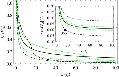
Numerical solution of Eq. (4) shows that Eq. (12) is quite accurate for . A simple interpolation expression for the screening potential of undoped graphene () can be obtained by replacing with in Eq. (12). The screening potential then satisfies the correct boundary conditions both at and at , and is close to the exact solution also for intermediate , see Fig. 2.footnote The best variational solution we found is
| (13) |
with and . The difference between the numerical and variational solutions is for and for .
From the general criterion for validity of the semiclassical approximation, , where is the de Broglie wavelength,Landau:77 one can derive a condition defining the range of validity of the potential obtained from the TF model: . The latter condition also implies that the in-plane electric field is small compared to the field perpendicular to the graphene sheet, (as ), which completes the proof that graphene behaves as a nearly perfect metal within the TF approximation. Using Eq. (13), and taking a typical boundary potential eV (Table 1) and effective dielectric constant for graphene on a SiO2 substrate,Ando:jpsj06 we find that the TF theory is valid for with the lattice parameter of graphene. Using high substrates will weaken this condition, making the TF results valid up to the immediate proximity of the metal contact.
Recently we described how depositing graphene on a metal surface leads to charge transfer between the metal and graphene. Giovannetti:prl08 ; Khomyakov:prb09 The graphene device shown in Fig. 1 consists of two regions, metal-covered graphene () and “free” graphene (). The sign and level of doping of metal-covered graphene is fixed by the first metal layer (M1), .Giovannetti:prl08 ; Khomyakov:prb09 The doping of graphene near the contact, , is determined by the boundary potential , see Eq. (13), which depends on the work function of the graphene-covered metal (M1) and the top metal layer (M2), see Eq. (7). If an abrupt - junction should form close to the contact at , see inset in Fig. 2. footnote3 and having the same sign but a different size results in - or - junctions. Such junctions break the electron-hole symmetry in graphene, giving rise to an asymmetric resistance as a function of the gate voltage.Huard:prb08 ; Cayssol:prb09 ; Farmer:nl09
At a distance the induced charge is determined by the top metal layer (“Metal 2”), , whereas far from the contact, , graphene is unaffected by the metal electrode. Using the work functions calculated in Ref. Khomyakov:prb09, , the boundary potential and junction type expected for different metal contacts are listed in Table 1, assuming the metal surfaces are clean. Because of the sensitivity of work functions to surface contamination, the contact potentials may be different for experiments that are not performed under ultrahigh vacuum conditions.footnote2
III.2 Doped graphene
Real graphene samples are often doped with some form of charged impurities. Eq. (12) shows that the screening potential is relatively unchanged by doping for a graphene region where , and asymptotically behaves as for , see Fig. 3, i.e. the screening is enhanced by doping.
Eq. (12) reveals an interesting effect related to the sign of doping. The screening potential is different for graphene doped with electrons and holes due to a - junction formation at for as shown in Fig. 3. The formation of the p-n junction for is caused by the competition between the charges of opposite sign induced by the metal contact and the charged impurities, respectively. The screening charge and potential for () are constrained by the metal contact (the charged impurities). The screening at is then suppressed, which gives rise to increase of the screening potential at the p-n junction as compared to the case of .footnote0 For the charges induced in graphene by the metal contact and the charged impurities are of the same sign so the overall effect leads to enhancement of the screening, reducing the induced potential. The asymmetry reaches its maximum at a critical doping level and vanishes upon increasing (decreasing) , i.e. for (). This effect should be observable in transport measurements where the impurity doping is gradually changed from - to -type.Farmer:nl09
III.3 Gated graphene
One can also create - junctions by applying a gate voltage (Fig. 1). Cheianov:prb06 ; Zhang:prl08 ; Fogler:prb08 Eq. (10) shows that the first effect of gating graphene is to cause a constant shift of the induced charge density. Secondly, the charge depletion width can be varied by changing the gate voltage since . This accounts for the electric field effect on the work function of graphene.Yu:nl09 Thirdly, a gate voltage applied to graphene creates qualitatively different junctions (-, -, - or -) at the contact region depending on the sign of the voltage. This will then lead to an asymmetry in the transport characteristics of the graphene device rather similar to the contact-induced abrupt junctions discussed in the last two paragraphs of Sec. III.1.
The point that separates and -doped regions of graphene, is given by . Eq. (10) yields . The screening potential near the transition point can be calculated using TF theory. The semiclassical description, however, breaks down exactly at since there are no screening charges at this point. The quantum corrections to the TF theory are, nevertheless, relatively small in graphene. DiVincenzo:prb84 ; Zhang:prl08 ; Fogler:prb08
According to our analysis, gating graphene (or impurity doping) can create an -- junction for some metal electrodes (Ni, Co, Pd, Ag, Cu, Ti/Pd and Ti/Au), see Table 1 and Fig. 2. This is possible because the sign of the graphene doping beneath the electrode, near the contact and far from the contact is independently fixed by the bottom metal layer, the contact potential and the gate voltage (impurity doping), respectively.
IV Conclusions
We have studied the electrostatic barrier formed in graphene in response to a metal strip in contact with the graphene sheet. By comparison with conventional metals, the screening in graphene is strongly suppressed: the induced electrostatic potential decays weakly with the distance from the metal contact as and for undoped and doped graphene, respectively. This leads to a substantial space charge region in graphene, breaking its spatial homogeneity. The latter has been recently observed by scanning photocurrent microscopy,Lee:natn08 and might also be seen for graphene in the quantum Hall regime.Shikin:prb01 ; Giesbers:apl08 The contact effects also result in the formation of a -, - or - junction at the near contact area that breaks the electron-hole symmetry and contributes to the contact resistance.Huard:prb08 ; Farmer:nl09 ; Cayssol:prb09 ; Yu:nl09 ; Giesbers:apl08 We predict that -- junctions can be realized by gating graphene or by impurity doping in combination with specific metal electrodes.
This work was financially supported by the “Nederlandse Organisatie voor Wetenschappelijk Onderzoek (NWO)” via the research programs of “Chemische Wetenschappen (CW)” and the “Stichting voor Fundamenteel Onderzoek der Materie (FOM)”.
References
- (1) K. S. Novoselov, A. K. Geim, S. V. Morozov, D. Jiang, M. I. Katsnelson, I. V. Grigorieva, S. V. Dubonos, and A. A. Firsov, Nature 438, 197 (2005).
- (2) Y. B. Zhang, Y.-W. Tan, H. L. Stormer, and P. Kim, Nature 438, 201 (2005).
- (3) M. I. Katsnelson, K. S. Novoselov, and A. K. Geim, Nat. Phys. 2, 620 (2006).
- (4) V. M. Karpan, G. Giovannetti, P. A. Khomyakov, M. Talanana, A. A. Starikov, M. Zwierzycki, J. van den Brink, G. Brocks, and P. J. Kelly, Phys. Rev. Lett. 99, 176602 (2007).
- (5) G. Giovannetti, P. A. Khomyakov, G. Brocks, P. J. Kelly, and J. van den Brink, Phys. Rev. B 76, 073103 (2007).
- (6) B. Huard, J. A. Sulpizio, N. Stander, K. Todd, B. Yang, and D. Goldhaber-Gordon, Phys. Rev. Lett. 98, 236803 (2007).
- (7) R. Danneau, F. Wu, M. F. Craciun, S. Russo, M. Y. Tomi, J. Salmilehto, A. F. Morpurgo, and P. J. Hakonen, Phys. Rev. Lett. 100, 196802 (2008).
- (8) E. J. H. Lee, K. Balasubramanian, R. T. Weitz, M. Burghard, and K. Kern, Nat. Nanotech. 3, 486 (2008); T. Mueller, F. Xia, M. Freitag, J. Tsang, and Ph. Avouris, Phys. Rev. B 79, 245430 (2009).
- (9) R. V. Gorbachev, A. S. Mayorov, A. K. Savchenko, D. W. Horsell, and F. Guinea, Nano Lett. 8, 1995 (2008).
- (10) E. Rotenberg, A. Bostwick, T. Ohta, J. L. McChesney, T. Seyller, and K. Horn, Nat. Materials 7, 258 (2008).
- (11) V. V. Cheianov and V. I. Fal’ko, Phys. Rev. B 74, 041403 (2006).
- (12) D. P. DiVincenzo and E. J. Mele, Phys. Rev. B 29, 1685 (1984).
- (13) M. I. Katsnelson, Phys. Rev. B 74, 201401 (2006).
- (14) L. M. Zhang and M. M. Fogler, Phys. Rev. Lett. 100, 116804 (2008).
- (15) M. M. Fogler, D. S. Novikov, L. I. Glazman, and B. I. Shklovskii, Phys. Rev. B 77, 075420 (2008).
- (16) G. Giovannetti, P. A. Khomyakov, G. Brocks, V. M. Karpan, J. van den Brink, and P. J. Kelly, Phys. Rev. Lett. 101, 026803 (2008).
- (17) P. A. Khomyakov, G. Giovannetti, P. C. Rusu, G. Brocks, J. van den Brink, and P. J. Kelly, Phys. Rev. B 79, 195425 (2009).
- (18) B. Huard, N. Stander, J. A. Sulpizio, and D. Goldhaber-Gordon, Phys. Rev. B 78, 121402(R) (2008).
- (19) J. Tworzydlo, B. Trauzettel, M. Titov, A. Rycerz, and C. W. J. Beenakker, Phys. Rev. Lett. 96, 246802 (2006).
- (20) S. Barraza-Lopez, M. Vanević, M. Kindermann, and M. Y. Chou, Phys. Rev. Lett. 104, 076807 (2010).
- (21) T. Ando, J. of Phys. Soc. of Japan 75, 074716 (2006).
- (22) A. D. Polyanin, “Handbook of Linear Partial Differential Equations for Engineers and Scientists” (Chapman & Hall/CRC, 2002), Eqs. 7.2.2-5 and 7.2.2-12.
- (23) L. D. Landau and E. M. Lifshits, ”Electrodynamics of Continuous Media” (Pergamon Press, 1984).
- (24) V. B. Shikin, Phys. Rev. B 64, 245335 (2001).
- (25) In principle, a similar interpolation procedure can be applied for the screening potential of doped graphene by replacing with in Eq. (12), where and .
- (26) L. D. Landau and E. M. Lifshits, ”Quantum Mechanics: Non-Relativistic Theory” (Pergamon Press, 1977).
- (27) The potential near the contact, and , will be very sensitive to the atomic structure of the metal (M1) electrode. However, this will not affect the asymptotic behavior of the potential, , at since the contribution to the TF screening potential from this small region, , is of higher order, , see Ref. footnote2, .
- (28) D. B. Farmer, R. Golizadeh-Mojarad, V. Perebeinos, Y.-M. Lin, G. S. Tulevski, J. C. Tsang, and Ph. Avouris, Nano Lett. 9, 388 (2009).
- (29) R. Golizadeh-Mojarad and S. Datta, Phys. Rev. B 79, 085410 (2009); J. Cayssol, B. Huard, and D. Goldhaber-Gordon, Phys. Rev. B, 79, 075428 (2009).
- (30) In some experiments the charged impurities might screen the potential such that the region where the contact potential is non-zero gets narrowed down to a small area near the contact, . Since the boundary potential then is , the screening potential behaves as for and for .
- (31) We note that the screening for is even less efficient as compared to undoped graphene () in the region of , see Fig. 3.
- (32) Y.-J. Yu, Y. Zhao, S. Ryu, L. E. Brus, K. S. Kim, and P. Kim, Nano Lett. 9, 3430 (2009).
- (33) A. J. M. Giesbers, G. Rietveld, E. Houtzager, U. Zeitler, R. Yang, K. S. Novoselov, A. K. Geim, and J. C. Maan, Appl. Phys. Lett. 93, 222109 (2008); P. Blake, R. Yang, S. V. Morozov, F. Schedin, L. A. Ponomarenko, A. A. Zhukov, R. R. Nair, I. V. Grigorieva, K. S. Novoselov, and A. K. Geim, Solid State Comm. 149, 1068 (2009); S. Russo, M. F. Craciun, M. Yamamoto, A. F. Morpurgo, and S. Tarucha, Physica E 42, 677 (2010).