Overview of Studies on the
SPIROC Chip Characterisation
R. Fabbri1, B. Lutz1, W. Shen2
1 DESY, Hamburg
2 University of Heidelberg
1 Introduction
The requirements imposed by the high precision physics forseen at the International Linear Collider (ILC) set high demands on calorimetry. The ambitious required jet energy resolution of [1] could be achieved by combining the potentials of the particle flow approach [1] with extremely segmented (in both transverse and longitudinal directions) electro-magnetic (ECAL) and hadronic (HCAL) calorimeters.
The ECAL design is based on a Si-W sampling structure with sensitive silicon pads of cm2 surface. The prototype will consist of approximately channels. A group of the CALICE collaboration has developed the analog option for the hadronic calorimeter (AHCAL) based on a sampling structure with scintillating tiles (of smallest size xx cm3) individually readout by Silicon Photo-Multiplier (SiPM) mounted on each tile.
The SiPM is a pixelated avalanche photo-diode operated in limited Geiger mode. The detector surface typically of few mm2 is divided into hundreds to thousands pixels. The analog output is obtained by adding the response of all pixels firing as independent digital counters. SiPMs are operated at - volts overvoltage. Given an internal pixel capacitance of typically fF, the charge collected for one photoelectron signal is approximately pC (equivalent to electrons). The SiPM offers a very fast response with a typical rise time of - ns. The dynamic range is determined by the finite number of pixels and reaches pC.
In order to test the feasibility of the particle flow approach prototypes of both ECAL and HCAL are being built by the CALICE collaboration and being tested in a combined test beam experiment. To meet the needs of the analog HCAL prototype it was decided to adapt the design developed for the ECAL front-end electronics to read the SiPM signal. This ILC-SiPM ASIC has been used during the test-beam runs at CERN and FNAL in 2006-07 and 2008-09, respectively. SPIROC is an evolution of the ILC-SiPM to be used for the next generation of ILC AHCAL prototype. In the following the main features of the new ASIC, version SPIROC 1B, proposed for the readout are described and its properties analysed. More specificately, the results on the analogue part of the chip are presented in this work. When reading out signals from photon detectors, SiPMs from MEPhy/Pulsar, identical to the devices used in the AHCAL test beam operations, were used. These SiPMs have a x mm2 surface divided into pixels.
The on going investigation of the digital component of the ASIC, implemented in the version SPIROC 2, will be presented in a separate future note.
2 SPIROC ASIC Description and Properties
The SPIROC chip is a dedicated very front-end electronics for an ILC prototype hadronic calorimeter with silicon photomultiplier readout. This ASIC has been designed and developed by OMEGA at Orsay [2].
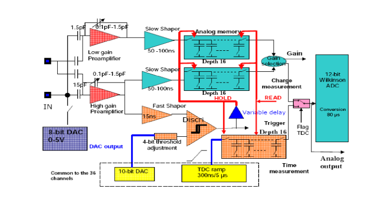
SPIROC was submitted in Fall 2007 and being tested since then. It embeds cutting edge features that fulfil ILC final detector requirements. It has been realised using AMS SiGe technology, and developed to match the requirements of large dynamic range, low noise, low power consumption, high precision and large number of readout channels needed. SPIROC is an auto-triggered, bi-gain, -channel ASIC which allows to measure on each channel the charge from one to photoelectrons and the signal timing with a ps accuracy TDC. The integrated ASIC components allow selectable pre-amplification gain factors (with output gain values from to mV/pC), and seven CR(RC)2 shaping times from to ns. After shaping, the signal is held at its maximum amplitude with a track and hold method. For each channel, an analogue slots memory array is used to store the time information and the charge measurement, and a -bit Wilkinson ADC has been embedded to digitise the analogue memory content (time and charge for the two gain modes). The data are then stored in a kbytes RAM. A very complex digital part has been integrated to manage all theses features and to transfer the data to the data acquisition system. An adjustable -bit DAC (- V) in the ASIC allows individual adjustment of the SiPM forward voltage for each one of the channels.
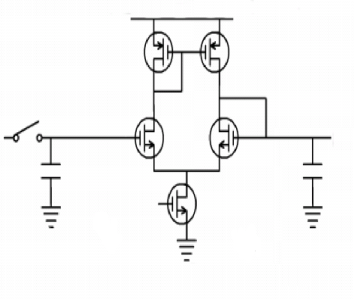
A schematic view of a single channel of the ASIC chip is given in Fig. 1.
3 Test-Bench Description
The characterisation measurements of the SPIROC chip were performed at DESY. The typical set up of the test bench is shown in Fig. 2.
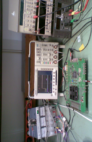

A digital pulse voltage generator (STS DG535) provides a rectangular signal at kHz rate and with variable amplitude up to V. Additionally, a dB attenuator ( factor attenuation) is inserted in the signal line. To simulate a real current signal from SiPMs, the generated squared signal is driven through a coupling capacitor ( pF) and a resistor ( ) located before the input channels in the SPIROC board, resulting in a characteristic decay time ns for the current signal.
The signal is then injected in one of the input channels, and the processed output signal can be measured either at the oscilloscope (Tektronix TDS , running at MHz bandwidth with Gs/s sampling rate) or directly via an external ADC module (CAEN ), accommodated in a VME create (CAEN ). The data acquisition is performed via a LINUX machine connected to the VME crate. The pulse generator is also connected to the LINUX machine, and is driven by scripts, allowing, together with the acquisition, for automatic, flexible, and systematic measurements in a large parameters space using SHELL scripts. Via an USB connection the chip is driven by a LabView user interface running under WINDOWS because the USB driver to steer the chip is not available for LINUX systems. This restricts the automation and flexibility of the measurements performing the scan of the ASIC related parameters. The porting of this software to a LINUX platform is ongoing.
A buffer amplifier, built at DESY, was often used (before the ADC input channels) to improve the precision of the measurement, as in the noise studies.
4 Electrical Noise Investigation
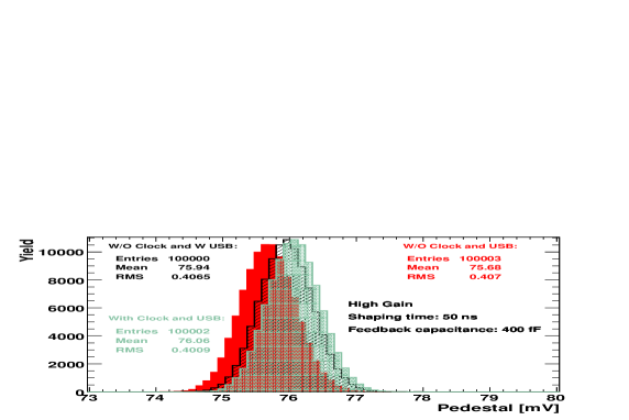
The noise affecting the processed signal out of the board was measured at different working conditions of the chip. Additional sources can superimpose to the chip noise during the measurement, as the USB-connection to the computer driving the board, the clock on the board which handles the input/output communications with the computer, and the connections to the pulse generator for the input and hold signals.
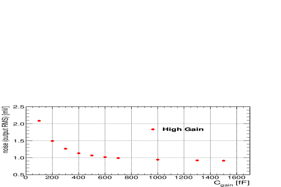
After disconnecting these additional noise source from the board, the noise was measured as the RMS of the analogue output signal. The dependence of the noise on the variable capacitance in the preamplifier stage of the chip is shown in Fig. 3, for both high and low gain operation modes.

The expected dependence in the high gain mode is observed. The noise reaches its asymptotic value for the largest feedback capacitance investigated value. For the low gain mode, where the amplification is one order smaller than for the high gain mode, no dependence is visible, being the noise dominated by the either the chip or the experimental board (the noise from the external ADC module was measured to be up to mV).
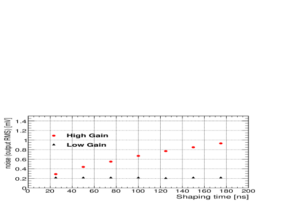
The dependence of the chip noise on the shaping time values is presented in Fig. 4. An almost linear dependence in the high gain mode is observed, while for the low gain mode no dependence is visible, similarly to what observed for the dependence on the feedback capacitance.
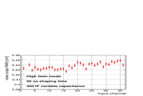
The uniformity of the noise in the SPIROC input channels was also investigated, and the result of the measurement is presented in Fig. 5, for the chip operating in high gain mode, at ns shaping time, and fF variable capacitance in the pre-amplifier stage. The measured noise is uniform within fractions of millivolts, well enough for the chip purposes. Although the upper half of channels appears to have a higher noise, this feature was not furtherly investigated being the effect negligible.
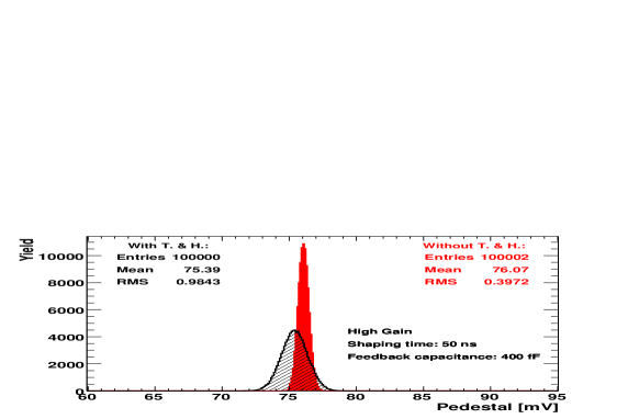
The largest effect superimposed to the electrical noise is given by using the track and hold switch to hold the pre-amplified and shaped signal at its peaking amplitude. An increase of the noise up to a factor - is observed in the output signal, Fig. 6.
With the used setup we could not distinguish between an increase of the noise or of the sensitivity to the noise (due to the increased bandwidth induced by the track and hold switch). Instead, a negligible effect is observed by the switching on the internal clock for input/output communication with an external driving interface (via USB port), and by plugging the USB connector into the board, Fig. 7.
In normal data taking conditions the ASIC is supposed to process the incoming signals via the track and hold component switched on. Therefore it is important also to measure its impact on the measured noise dependence on the preamplifier gain, Fig. 8.
Consistently with what shown in Fig. 6, an increase of the noise up to approximately a factor is observed at fF.
5 ENC and Input Detector Capacitance
Sofar the electrical noise of the stand-alone ASIC was investigated, without any input signal line connected to the board. Connecting a SiPM to the readout system is expected to increase the noise, depending on the detector capacitance.
In principle, a charge-sensitive preamplifier would be favoured [5], providing small sensitivity to changes of the parasitic capacitance at its input, as in the case of SiPMs whose capacitance changes with temperature. Nevertheless, in order to cover the large dynamic range of SiPMs, a voltage-sensitive preamplifier was adopted for the chip. It is crucial therefore to quantify the noise sensitivity to an external variable capacitance coupled via the connected detector.
Since the signal from the SiPM appears as electric charge, electronic noise will be quantified by giving its ’equivalent noise charge’ (ENC), defined as the input charge which would be necessary to generate a signal equivalent in amplitude to the measured noise output of the ASIC. This value can be obtained by normalising the noise to a reference signal. As an example, the signal originating from one photo-electron in the SiPM, and its corresponding output are considered. Assuming a SiPM gain of order would result in an input charge approximately of fC. The corresponding output signal for the highest gain was found to be mV (see Sec. 16), obtaining an ENC of order
| (1) |
Here is the average voltage noise level (in millivolt) appearing at the output. Dividing it by the the electron charge (in femtocoulomb units) gives the ENC in number of electrons
| (2) |
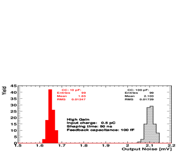
Using the external pulse generator, the output noise was measured and converted in number of equivalent electrons following the above formula (2). During the measurement, the coupling capacitance value was varied to simulate the change of the SiPM internal capacitor. The results of two scans performed in sequence, without any change in the setup apart replacing the capacitor, are presented in Fig. 9,
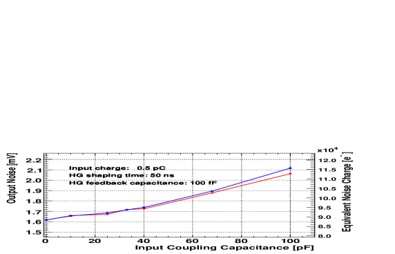
showing a noise increase up to in the range - pF, from to mV (corresponding to an ENC variation from to electrons). According to these measurements, the signal over noise ratio achievable by the SPIROC can be calculated, ranging approximately between and assuming a SiPM of .
To verify that the observed non-reproducibility of the measurements is not given by any feature of the ASIC, a series of measurements was taken in sequence at a fixed coupling capacitance to simulate the detector capacitance. No additional change in the experimental apparatus was introduced. The results for two values of the coupling capacitance, Fig. 10, shows a spread in the measurement which is of the order of a fraction of millivolt. This is well below the maximum spread observed in the two consecutive scans, thus suggesting a noise source external to the ASIC, possibly due to the experimental setup.
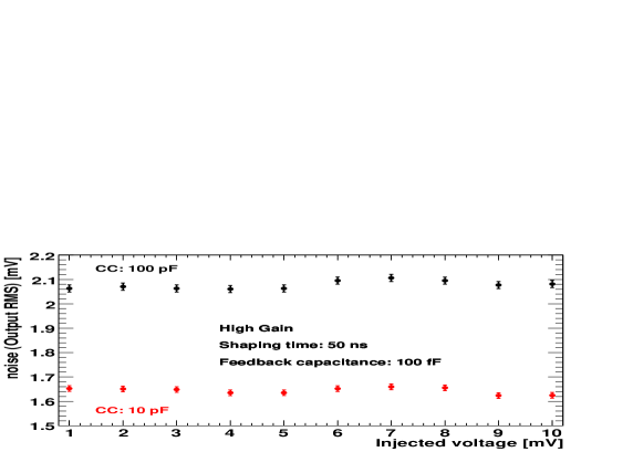
The measurement of the coupling capacitance dependence of the ENC was performed injecting pC into the ASIC (except for the measurement at zero capacitance, when the line was disconnected from the board). To validate the results it should be verified the reasonable assumption that the measured noise is not influenced by the amount of injected charge. A measurement of the noise was taken at different values of injected charge, and for two values of the coupling capacitance, showing, as expected, no dependence, Fig. 11.
6 Pedestals Uniformity
Pedestals were investigated for all the the input channels of the chip, to verify their uniformity, and are presented in Fig. 12, using the external ADC module.
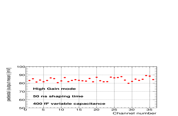
Note that the mean values reported here are not the absolute pedestal values, due to an offset introduced for convenience in the amplifier before the ADC.
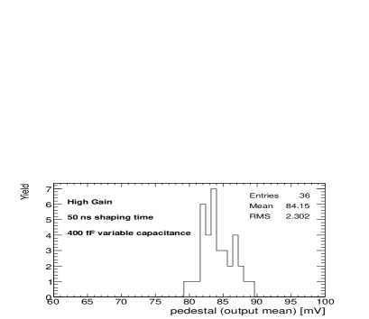
The measured spread of pedestals is about mV, Fig. 13, a value slightly larger than what reported in [2].
7 Trigger Discriminator and Efficiency
The chip is designed to operate in the so called ’auto-trigger’ mode. The input signals are first pre-amplified according to both low and high gain line settings. In the high gain section a dedicated ns fast shaping line is also present in parallel to the line to the analogue memory. There the signal enters a discriminator with a threshold common to all input lines, and a ns wide trigger is generated whenever the voltage in the line is above the threshold value set, Fig. 1. The common threshold is tunable by a bits DAC. On top of the common threshold value, each channel threshold can be individually tuned via a -bit DAC.
In normal ILC operations the generated trigger is forseen to subsequently hold the pre-amplified signal, processed in the meanwhile by slower shapers, at its amplitude peaking value. It is therefore crucial to investigate the trigger efficiency and homogeneity for the channels.
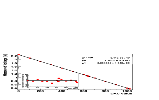
The calibration of the common DAC values was performed, and is shown in Fig. 14. The threshold is found to range from V up to V. The residuals to linearity, found to be within few millivolts (a fraction of a photon-electron signal), are presented in the small insert panel.
After having performed the discriminator DAC calibration, the trigger efficiency can be investigated channel by channel. This is done using a built-in procedure in the LabView user interface. The program increases the threshold level in sequence of DAC units, remains at a fixed DAC value for cycles, and counts the number of triggers generated by the pedestal of the investigated channel. It provides thus a measurement of the trigger efficiency, which is presented in Fig. 15
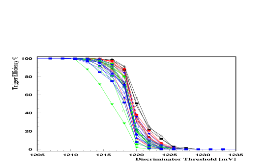
for an injected charge of fC, separately for each of the channels.
The increase of the trigger counting is smoothed by the noise amplitude in the line, which was typically found to be around - mV during that specific measurement, and was obtained considering the threshold value variation needed to increase the trigger efficiency from to . Also, the maximum efficiency is reached at threshold level values different from channel to channel, with a spread of around mV, resulting in a negligible pedestal spread between all the channels. During forseen data taking operations, the observed spread can, in principle, be cured tuning the discriminator level channel by channel using the forseen -bit threshold finer adjustment. At the moment, this feature is not properly working in the released versions of the chip (SPIROC 1 and SPIROC 2), and could not be investigated.
8 Trigger Time Walk and Jitter
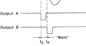
As mentioned in Sec. 7, SPIROC is forseen to be used in auto-trigger mode during ILC running conditions. It is crucial therefore to investigate the size of the main uncertainties which can affect the trigger timing. Signals with different amplitudes (and same peaking time) cross the discriminator level at different times, resulting in a time shift (trigger walk) of the generated processing trigger, left panel of Fig. 16. On top of this uncertainty, the crossing of the discriminator level is varied in time (trigger jitter) by the noise in the analogue signal, right panel of Fig. 16.

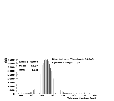
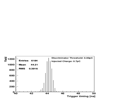
The trigger time walk and jitter were investigated injecting a signal from the pulse generator, and then measuring at the oscilloscope the timing of the coincidence of the generated trigger in the chip with the main pulse generator trigger. Different threshold values for the analogue signals were set (via the LabView interface) at the -bit DAC discriminator (common to the input channels) in the fast shaping line, and different charge values were injected, thus allowing for the study of the time walk and jitter dependence on the trigger threshold level and on the amplitude of the input signal. The shift of the mean and the RMS value of the measured trigger distribution, which is shown for a typical setting in Fig. 17, provide the measurement of the trigger time walk and jitter, respectively. Typical distributions of the trigger timing above described are presented in Fig. 18.

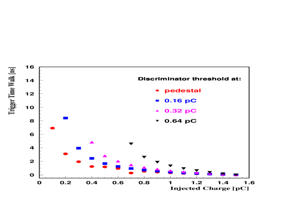
The results of the time walk measurements are shown in Fig. 19, for increasing values of the injected charge, from up to pC (equivalent to one pixel and firing pixels in an AHCAL SiPM, respectively), and of the discriminator threshold level. The time walk values are presented with respect to the trigger timing corresponding to the largest injected charge. When setting the threshold value above the pedestal the time walk appears to be up to ns only for the first pixel peaks. For a larger number of firing pixels it is within one nanosecond; this feature is observed also for a threshold at about half a mip (SiPMs are configured such that on average pixels should fire due to a mip energy deposition [3], thus corresponding to pC input charge).
The trigger jitter dependence on the injected charge, for different values of the discriminator threshold, is presented in Fig. 20.
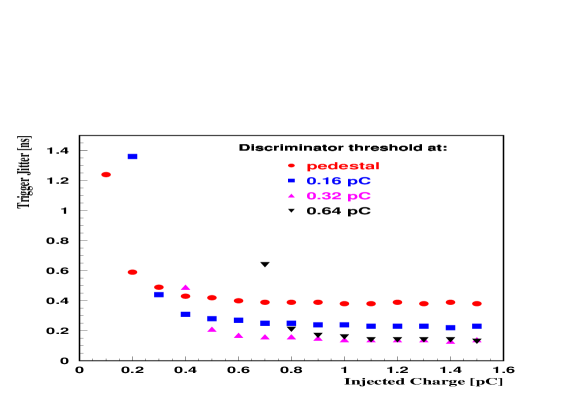
The jitter appears to be up to ns, at the smallest threshold values and for small values of injected charge, while it is within ns at a threshold of about half a mip.
Concerning the forseen operation of the chip in auto-trigger mode, resolving single-pixel structure in the SiPM spectra (i.e., in calibration mode) appears to be not infeasible, due to the reasonably small measured trigger jitter and time walk At the moment, the SiPM calibration is expected to be performed via an LED system providing an external trigger to the ASIC readout. This issue will be extensively presented in Sec. 15. Instead, the small time walk and jitter values observed at thresholds and input charges above half a mip, should definitely allow the chip to properly operate in the physics mode. The influence of largely varying SiPM gain values, light generation and collection efficiency has not been studied in this work.
9 SiPM Voltage Adjustment
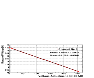
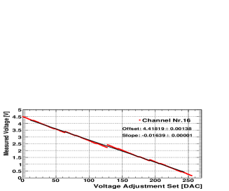
The chip is forseen to be connected to an external power supply and to provide a common high voltage bias to all connected SiPMs. Tuning of the applied voltage, channel by channel, is achieved using an -bit DAC HV adjustment dedicated to each detector power line, Fig. 21.

The calibration of the input HV DAC for all channels is at the moment performed via dedicated LabView interface routines. The applied voltage ranges approximately from V to V, varying from channel to channel, Fig. 22.

The measurements are linearly fitted in the range 10-245 DAC units, and the residual of each measurement to the resulted linear function is calculated. A large channel by channel variation in the residuals size is observed, and two extreme cases are reported in Fig. 23.
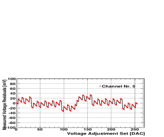
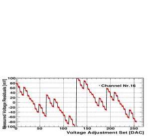
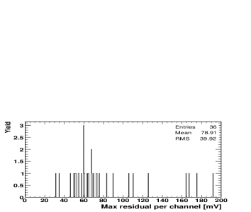
The results show a differential non-linearity on average up to mV, and for some channels up to mV, Fig. 24, resulting in a relative gain change of approximatively and [4], respectively, and thus providing a potential systematic uncertainty of similar size to the energy calibration of the detector,
in case the observed deviation cannot be systematically reproduced.
To investigate the reproducibility of the voltage tuning applied to the ASIC channels, two series of DAC scans (five scan per series) were performed for one channel in separate periods characterised by a temperature variation of three degrees Celsius. Within each data set, the maximum deviation between the measured voltage values was calculated for each DAC value, and is presented in Fig. 25.
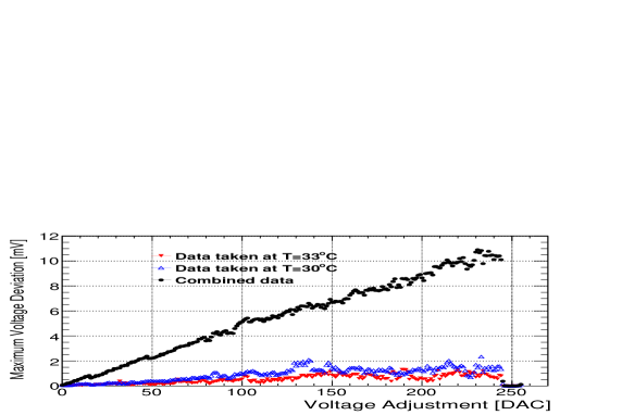
As expected, for each series of measurements the spread increases with the DAC value, i.e. with the amount of current in the DAC switch, resulting in a maximum systematical deviation up to one millivolt. As a consequence, the observed large differential non-linearity can be corrected via a calibration of channel by channel HV adjustment DAC.
Although a negligible deviation is observed among the measurements, when combining the two data sets the maximum spread of the measurements increases up to mV. This can be possibly interpreted as due to the large variation of the temperature (up to three Celsius degrees) measured during the systematical studies, resulting in a larger applied voltage value observed at a lower temperature. In this case, the observed change of voltage adjustment value could be corrected via a proper calibration. The calibration might not be needed in case of small temperature gradient during data taking, since the observed mV systematical spread is still small compared to the overvoltage of SiPMs, typically of - V for the devices used in current AHCAL test beam operations [4]. Thus, this spread would correspond to a gain change below %.
10 Low Gain - High Gain Coupling
In each input channel of the ASIC the low and high gain paths are electrically coupled, Fig 26.

As a result, the charge sharing between the two paths is influenced by the feedback capacitance value set.
In order to estimate the effects of the high-low gain coupling, the output signal in one path was measured for different capacitance values in the other preamplifier line. No significant effect is observed in the output signal of the high gain line while changing the amplification in the other line. Instead, a sizable effect (up to ) is visible when measuring the output signal in physics mode and changing the amplification in the high gain line. An example of the observed correlation is presented in Fig. 27 for different values of the charge injected in the ASIC (using a dB attenuator at the pulse generator output).
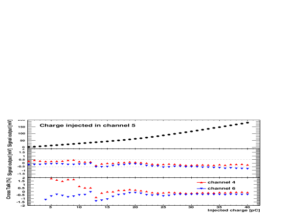
11 Cross Talk between Input Channels
The chip will handle incoming signal lines. According to previous measurements [2] the estimated cross-talk among the neighbouring channels is below for an injected charge of pC. The measurement in [2] was presented for few injected charge values only. This investigation of the cross-talk was done performing a wider scan of injected charge. While increasing the injected charge in steps of pC from one to pC, corresponding approximately to the range mips, the output signal (pedestal subtracted) was measured in the neighbouring channels. The ASIC was run in low gain mode (physics mode) at ns of shaping time, and fF of feedback capacitance.
An example of the performed measurements is presented in Fig. 28. The output signal in the line where the charge was injected is shown in the upper panel. The reason of the observed non-linearity was found in the track and hold switch (see Sec. 12). In the neighbouring lines the measured signal is typically within mV in the analysed input charge range (middle panel), confirming a negligible charge leakage between the channels. A small trend is visible, within the mV range, moving from small to large injected charge. For each charge value the cross-talk (bottom panel) in one channel was calculated dividing its signal (held at its maximum amplitude) to the corresponding signal in the line where the charge was injected. As expected by using this method, the cross-talk inflates at small input charge values. At the pC of injected charge, the measurement is close to what reported in [2].
12 Track and Hold Switch
The chip has to save the amplitude of the pre-amplified and shaped signal at its peaking time (arrival time of signal maximum). This is achieved using the track and hold switch, Fig. 29, which holds the signal at the amplitude corresponding to a provided holding-trigger arrival, to be tuned to hold the signal at its maximum amplitude.
The peaking time is not expected to depend on the amount of injected charge (mainly depending instead on the shaper type [6]), and the choice of the holding-trigger should hold for all values of input charge. Surprisingly, it was observed that the peaking time varies with the charge. The signal amplitude was measured with the external ADC while performing a scan of the holding-trigger arrival time, in both low and high gain modes, for ns shaping time, and for all possible values of the feedback capacitance. An example of these measurements is shown in Fig. 30. In these test-bench measurements the hold signal is generated by the external voltage source. Its arrival time can be arbitrarily varied to anticipate or delay it with respect to peaking amplitude of the injected charge.
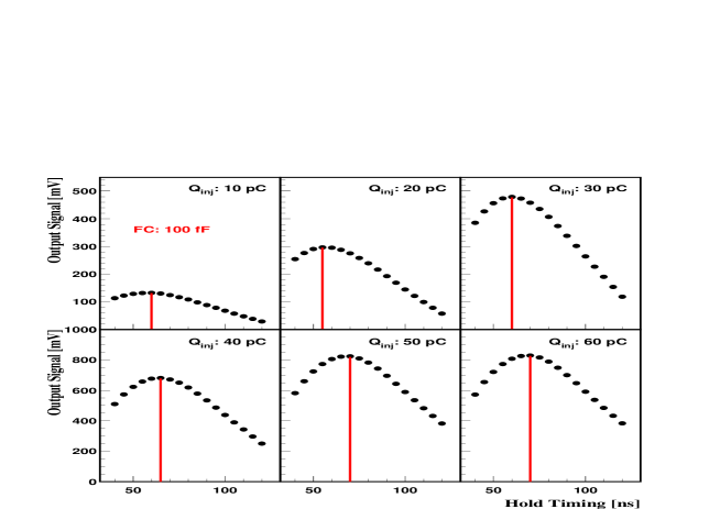
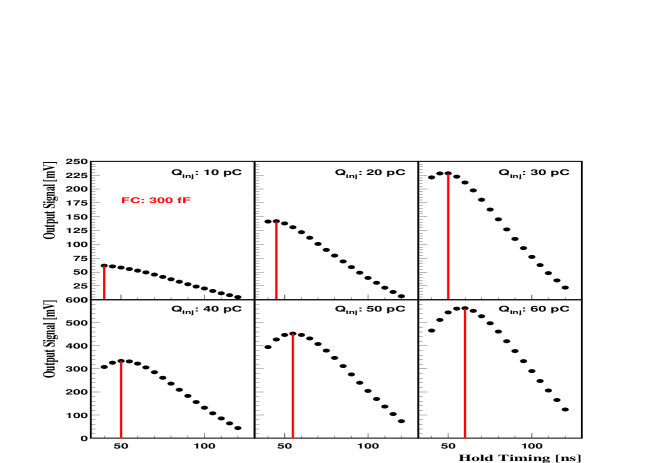
The measurements show that the peaking time (displayed with a vertical line in each plot) increases with increasing injected charge (while remaining constant only after reaching saturation), thus suggesting that either the peaking time is charge dependent (contrary to the expectations) or that the track and hold switch somehow interferes with the signal developing in time.
After investigation by the Orsay group, a possible explanation of the observed feature in the small charge region was proposed [7]. Due to the small bias transistor size in the track and hold buffer (bottom transistor in Fig. 29) and to the large parasitic capacitance at its output, small input charge will make the buffer enter the non-linear working region. The investigation with simulations is on-going by the Orsay group.
13 Dynamic Range, Linearity, and Gain of the ASIC
During normal AHCAL data taking (low gain) the dynamic range of the ASIC should cover the region between one mip and mips ( pixels per SiPM / pixels firing per mip), considering saturation effects in the SiPM due to the limit number of pixels and to the pixel recovery time. Assuming a SiPM gain of the order of (corresponding to pC charge generated per pixel), the covered dynamic mips range corresponds to the region between and pC. It should be noted that this upper charge limit depends on the specific photodetector gain (MEPhy/Pulsar devices, considered here, have a pixel gain variation between and ).
The chip preamplifier gain should be chosen such to provide a linear response in the whole energy range. On this purpose, a scan was performed over all feedback capacitance values possible in low gain mode, while increasing the amount of injected charge. For each input charge, it was chosen the hold-trigger timing corresponding to the maximum amplitude for the output signal measured at the external ADC. This choice was motivated by the impossibility of performing such a time consuming multi-parameter scan extracting the proper holding-time via the oscilloscope, without an automatised procedure (each single point of the scan was systematically measured several times). Systematic effects arising by the track and hold switch, as discussed in Sec. 12, might affects the results.
The results of this scan, presented in the upper panel of Fig. 31 for ns shaping time, indicate that the minimum feedback capacitance value needed to cover the required SiPM dynamic range ( mips) is fF. Above this value the maximum expected mip signal can be processed before the ASIC runs into saturation. As a reference, the values of the injected charge are also reported in terms of equivalent AHCAL mips values.
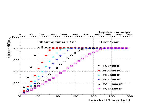
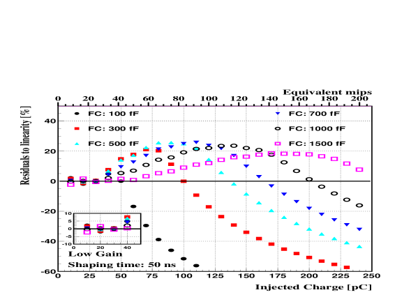
The sets of data were linearly fit in the range - pC and the residuals to the linearity were calculated dividing the deviation of the measured points from the fit results over the fit values. A non linearity up to is observed with increasing injected charge, bottom panel of Fig. 31. The region where the ASIC saturation appears (anyway not relevant for the forseen operation of the chip) shows a consistent drop of the residuals.
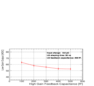
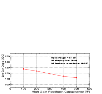
Similar measurements were performed operating the chip in high gain mode, Fig. 32.
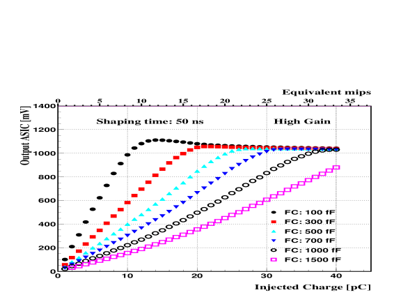
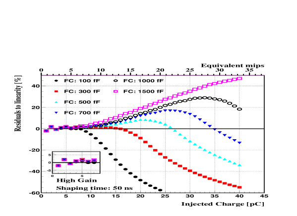
In this mode, used for calibration, it is preferable to use the largest (smaller) gain (feedback capacitance) to investigate the SiPM single-pixel spectra. The results show that for fF of feedback capacitance the saturation is reached for values of input charge above pC, corresponding to a dynamic range up to mips, enough for performing the calibrations. Note that here the linear fit was performed in the range - pC.
The observed non linearity is mainly due to the mentioned features of the track and hold switch, which are under investigation and will be possibly cured in the next generation of the chip. In addition to the observed injected charge dependence of the peaking time, it was also observed that the peaking amplitude obtained via the track and hold switch is typically larger than what observed when the signal is not held.
The gain of the chip was calculated out of the same data according to the formula (in units), and is presented in Fig. 33 for different values of the feedback capacitance in both low and high gain modes at ns shaping time.
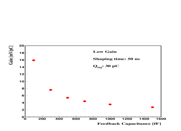
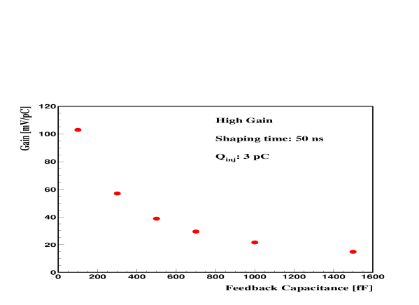
In the low (high) gain mode the chip amplification factor was measured for pC ( pC) of injected charge, a value not sizably affected by the non-linearity induced by the track and hold switch. The expected functional dependence of the gain [5] is observed, quantitatively in agreement with the measurements presented in [2] and [8].
14 Amplitude Dependence on Shaping Time
The effect of the shaping time value on the measured signal peaking amplitude was investigated. The amplitude was measured operating the ASIC in low gain mode for different values of the shaping time and for the feedback capacitance value of fF, Fig. 34.
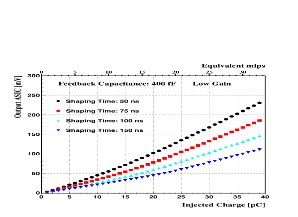
Differently from what presented in Fig. 31, here a dB attenuator was used, to present results at small injected charge in finer binning. Also, results are presented for charge values down to pC.
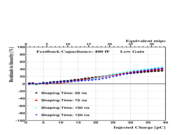
The signal peaking amplitude appears to increase with decreasing shaping time, in agreement with simulations. The sets of data were linearly fit in the range - pC and the residuals to the linearity were calculated dividing the deviation of the measured points from the fit results over the fit values. A non linearity up to is observed for increasing injected charge, bottom panel of Fig. 34. In this region of injected charge values the non-linearity response (due to the track and hold switch) appears to be weakly dependent on the chosen shaping time. Note that a direct comparison with the results presented in the bottom panel of Fig. 31 cannot be done, being different both the region considered in the linear fit and the smallest values of injected charge considered in these measurements.
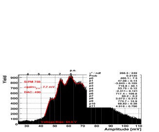
15 SiPM Single-Pixel Spectra
The possibility to operate the ASIC in auto-trigger mode during calibrations was shown to be feasible due to the low trigger jitter time walk, smaller than and ns, respectively (see Sec. 8). That possibility is confirmed by the following measurement of the single-pixel spectrum.
A SiPM, flashed by an LED, was connected to the board, and the processed output signal was investigated. The device was operated at overvoltage larger ( V) than the nominal value, to increase the cross-talk between the pixels (which is, on the other side, not desirable for physics mode operations). The SiPM signal was measured using the auto-trigger mode described in Sec.7. After properly setting a discriminator threshold value, the generated trigger was used to trigger an external pulse generator (HP 8082A). One signal from the pulser was then used to open the gate of the external ADC module, and a second signal was input to the SPIROC board to hold the analogue signal from the SiPM at its peaking amplitude.
When the discriminator threshold is set above the pedestal the contribution of the thermal noise dominates the measured spectrum, Fig. 35, due to its large rate (typically around MHz).
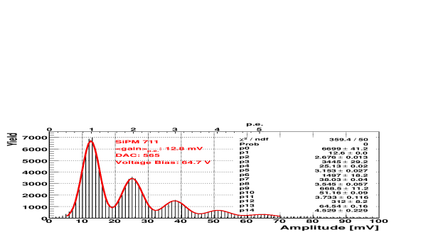
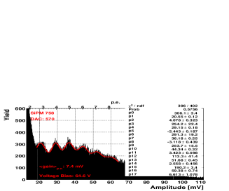
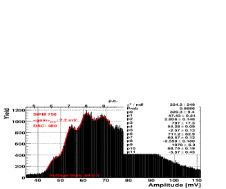
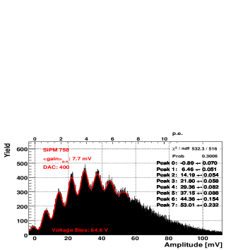
In order to observe the contribution of LED light induced events in the spectrum, the discriminator threshold was set to DAC units, corresponding to a value approximately above pixels for a measured gain of mV per pixel (operating the SiPM at V), Fig. 36.
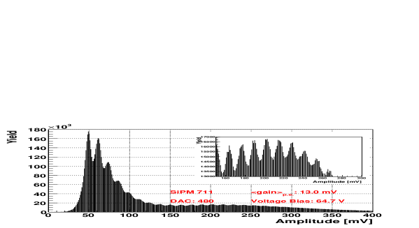
Also, the rate of the LED flashes was increased to kHz from the initial kHz. Although the thermal noise contribution appears to be still sizable in this experimental configuration (dominating the spectrum first peaks), the LED signal appears in the spectrum at large amplitude values, and is also presented in the zoomed panel of the picture. The results show the single-pixel structure, and suggest that a fit of the spectrum (either the thermal noise or the signal contribution) might be possible, although its quality cannot be quantified at this stage of the analysis.
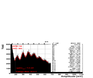
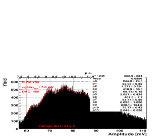
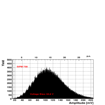
The above results were obtained for a quite large gain of the SiPM. To see the effects of a lower pixel gain value, the voltage bias applied to the device was decreased to V resulting in a gain around mV per pixel, which corresponds to approximately half a million electrons. The discriminator threshold value was kept unchanged, corresponding at about five pixels at this low pixel gain. The resulting spectrum is presented in Fig. 37.
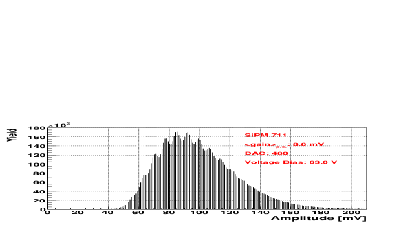
Due to the lower device gain and to the high discriminator threshold value the contribution from the thermal noise is here strongly suppressed, and the spectrum is mainly populated by LED driven events.
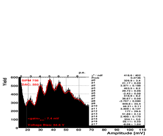
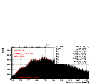
To see the quality of the noise spectrum for this low SiPM gain, the threshold was set above the pedestal, Fig. 38.
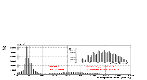
At this low pixel gain value, the single-pixel structure of the thermal noise spectrum appears to be deteriorated, complicating the possibility to perform a fit of the pixel structure to calibrate the device. This complication might be overcome by operating the SiPM with a larger gain, as shown in Fig. 35 .
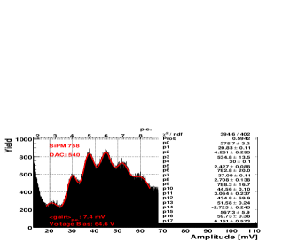
As a comparison, the measurement was repeated using an external trigger to hold the peaking amplitude and to open the gate of the ADC module, operating the SiPM at low pixel gain and setting the discriminator threshold value above the pedestal. The LED intensity was decreased to have a lower number of pixels firing, similarly to what is usually done calibrating a SiPM with an LED system. The single-pixel spectrum, now without any contribution from the thermal noise, is presented in Fig. 39.
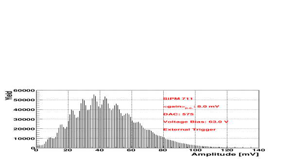
The peaks appear to be well separated, allowing the calibration of the device using an external light source system. Potentially, the calibration of the photodetector might be also performed running the SPIROC in auto-trigger mode by analysing the thermal noise. In this case, during the calibration the SiPM should be operated at larger pixel gains, as shown above.
16 Towards Real Data Taking Conditions
When the measurements presented in this note have been performed, the software to operate the chip in auto-trigger mode (see Sec. 7) was not fully implemented. This limitation could be somehow bypassed using the following procedure, thus testing the capability and the efficiency of the chip to perform

measurements in both physics and auto-trigger mode at different trigger threshold values, Fig. 40.
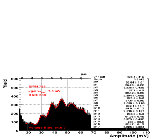
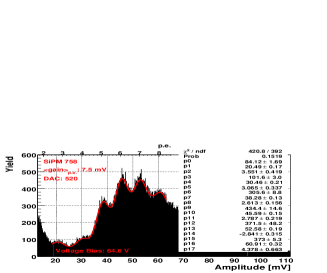
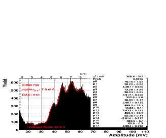
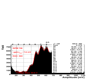
These measurements were performed using the signal from a SiPM (SiPM number 758), thus simulating, as much as possible, real data taking conditions. Spectra suitable for fitting the single-pixel structure of the signal were obtained operating the high voltage supply at V, corresponding to V voltage bias measured at the dynodes of SiPM by setting the input HV DAC tuning to zero units (see Sec. 9). Note that the nominal operation voltage for this SiPM is V, as declared in the SiPM database. The main pulse generator triggered the generation of a negative voltage pulse (via a Hewlett Packard pulse generator providing width, leading and trailing edges tunable down to the nanosecond level) to an LED, optically coupled to a SiPM whose signal was then directly input to the ASIC board, using the same high voltage line, Fig. 21. The intensity of the LED, and in turns of the SiPM signal, could be then regulated by the chained pulser.
During test-bench measurements the signal to open the ADC module gate is typically provided by the pulse generator, for every generated voltage pulse. Accessing the trigger allows instead to generate the open-gate signal only in case a processed signal (either from the thermal noise or from the LED) overshoots a chosen threshold value in the discriminator. The generated trigger was therefore used as an external trigger to an additional pulse generator, which in turns generated the signal to open the ADC module gate at a suitable time. The hold signal was provided by the main pulser used to switch the LED on.
As a first step, the chip was operated in high gain mode in parallel with low intensity LED light, while applying different threshold DAC values via the LabView interface (the larger is the DAC value set, the smaller is the applied threshold level value). Using the trigger only to open the ADC gate, but holding the signal peaking amplitude via the external primary pulse generator allowed to easily fit the single-pixel structure of the spectrum corresponding to LED events, for the purpose of this measurement, Fig. 41- 42.
In case a signal induced by thermal noise overshoots the discriminator threshold level then the ADC gate is still opened by the generated trigger but the processed signal is not any more synchronised with the hold signal generated by the main pulser. This results in deteriorating the single-pixel structure of the thermal noise contribution, and populating the spectrum towards the pedestal region (the recorded signal amplitude is lower than the real peaking amplitude). This contribution from thermal noise to the spectrum is increasingly suppressed with increasing the threshold value, as clearly visible in Fig. 41. Although the number of suppressed peaks in the spectrum increases by increasing the threshold level, the measurements show that a remaining small contribution from the peaks expected to be suppressed is still present. This feature, possibly due to the experimental setup, has not been furtherly investigated at this stage of the analysis, being not relevant for the measurement presented here.
From the above measurements the threshold values to cut specific spectrum peaks can be determined resulting in approximative DAC units per peak, Tab. 1. This corresponds to a step of mV in the fast shaping line (see Fig. 14).
| DAC value | Suppressed peak number |
As a cross check, a similar spectrum was taken using the pulse generator to open the ADC gate, obtaining the same single-pixel peak locations, Fig. 43.
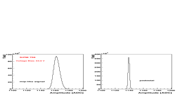
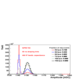
With the same setup, a mip signal was tentatively obtained tuning the LED amplitude such that the SiPM spectrum shows a maximum around the pixel peak amplitude, Fig. 44.
Keeping the same LED amplitude, the mip-like signal was then measured using the low gain mode of the chip, Fig. 45, for a shaping time of ns.
Using again the generated trigger to open the ADC gate, and applying different threshold DAC values, the trigger efficiency with respect to the signal discrimination level was investigated for two values of the feedback capacitance, Fig. 46.
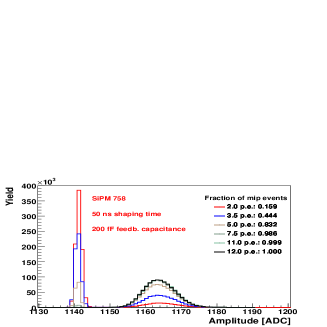
In the plots, the threshold DAC values are presented in terms of number of photo-electron peaks which are cut by the selected threshold, according to Tab. 1. By increasing the DAC value (decreasing the trigger threshold) the number of triggers generated by the noise increases, resulting in a larger contribution of pedestal events to the overall accumulated events in the spectra. Already at half a mip threshold the fractional contribution of SiPM signal events is almost , for both the investigated ASIC configurations.
The preliminary results presented here verify the possibility to operate the ASIC in auto-trigger mode (after the mentioned improvement of the track and hold switch) processing the physics events at half a mip cut on the trigger threshold, as forseen in the ILC applications.
17 Conclusions
During 2008 and 2009 systematic studies have been performed to characterise the analogue component of the SPIROC ASIC, designed for the readout of the analogue hadronic calorimeter for the international linear collider project. The more significant results are presented and described in this report showing the fulfilled requirements and the features which should be fixed in the next version of the chip. These measurements have been done on the SPIROC version SPIROC 1B, which has the analogue processing of signals almost fully implemented.
The ASIC was shown to handle the dynamic range covered by the SiPMs which are expected to be readout in both calibration mode for the maximum amplification at fF feedback capacitance, and physics mode for values of feedback capacitance above fF, resulting non-saturated up to and mips, respectively. The values reported here refer to a SiPM with pixel gain of order . In case of SiPMs with highly varying pixel gain (as for the SiPMs used in the past AHCAL test beam operations), the dynamic range covered by the photodetector changes, and the operation mode of the chip should be changed accordingly, resulting in a change of the signal over noise ratio.
The data acquisition is forseen to run in auto-trigger mode, being activated by the SiPM signals, and the chip appears to fulfil this requirement in the physics mode, reaching trigger efficiency for trigger threshold values above half a mip. For these values the trigger time walk and jitter were found to be less than and ns, respectively. Quite remarkable, is the observed possibility to fit the thermal noise, opening the potentiality of self-calibrating the device.
The electronic noise was investigated and found to be typically within one millivolt, depending on the specific shaping time and amplification setting. The most sizable additional contribution to the noise is induced by switching on the track and hold component, approximately doubling the noise. When coupled to an external signal source the noise dependence on varying the coupling capacitance (as for real SiPMs) was found to be within in the range - pF.
Comparing the input channels, the pedestals showed a spread of mV, and their deviation due to cross-talk was measured to be within mV in the investigated range from one to mips ( pC).
Each input SiPM high voltage can be individually tuned via a DAC HV adjustment dedicated to each detector line. The DAC to volt calibration was performed for all channels showing a channel to channel average variation of mV, and an average maximum deviation to linearity of mV (for some channels up to mV). The observed deviation from linearity appears to be systematically reproducible, and could be corrected for via a proper calibration.
The high-low gain path coupling was studied and a sizable dependence (up to ) on the high gain amplification setting was measured for the physics mode readout.
Probably the most surprising feature of the chip was the observed increase of the signal peaking time with increasing injected charge, related to properties of the used track and hold switch. Investigation with simulations by the chip designers in Orsay is on-going, and a possible cure of the shown feature should be available in the next generations of the ASIC.
The investigation of the digital component of the ASIC, implemented in the version SPIROC 2, is on going and will be presented in a separate future note.
Acknowledgments
We are deeply grateful to S. Callier, C. De La Taille, and L. Raux of the OMEGA group at Orsay, and to F. Sefkow and E. Garutti at DESY for useful discussions and suggestions.
References
- [1] J. Brau et al., International Linear Collider Reference Design Report, ILC-REPORT-2007-001 (2007).
- [2] M. Bouchel et al., Proc. of the IEEE 2008 Nuclear Science Symposium, Dresden, Germany, October 2008.
- [3] M. Groll, Construction and Commissioning of a Hadronic Test-Beam Calorimeter to Validate the Particle-Flow Concept at the ILC, PhD Thesis 2007, DESY-THESIS-2007-018.
- [4] N. Feege, Silicon Photomultipliers: Properties and Application in a Highly Granular Calorimeter, Diploma Thesis 2008, DESY-THESIS-2008-050.
- [5] W. R. Leo, Techniques for Nuclear and Particle Physics Experiments, Springer-Verlag.
- [6] E. Kowalski, Nuclear Electronics, Springer Verlag.
- [7] L. Raux, private communications.
- [8] L. Raux, SPIROC ASIC Measurement, Presentation given at CALICE ELECTRONICS meeting, March 11, 2008.