Anisotropic Magneto-conductance of InAs Nanowire: Angle Dependent Suppression of 1D Weak Localization
Abstract
The magneto-conductance of an InAs nanowire is investigated with respect to the relative orientation between external magnetic field and the nanowire axis. It is found that both the perpendicular and the parallel magnetic fields induce a positive magneto-conductance. Yet the parallel magnetic field induced longitudinal magneto-conductance has a smaller magnitude. This anisotropic magneto-transport phenomenon is studied as a function of temperature, magnetic field strength and at an arbitrary angle between the magnetic field and the nanowire. We show that the observed effect is in quantitative agreement with the suppression of one-dimensional (1D) weak localization.
pacs:
73.63.Nm, 72.20.My, 73.20.FzIn the past two decades, semiconductor nanowires have attracted much attention due to their great potential in both fundamental research and novel device applications. They are considered as versatile building blocks for future nanoelectronics Lieber ; thelander , and as a platform to explore the fundamental physical properties of quasi-1D Luwei ; smallSiNW or zero-dimensional (0D) systems bjork ; xiangjie ; yongjie ; InAsQDspinorbit ; NWholespin ; nanowireQD1 ; nanowireQD2 . Moreover, the quasi-1D nature of semiconductor nanowires may help to achieve significant enhancement in thermoelectric performance NWTEtheory ; NWTE1 ; NWTE2 . Thus it is highly desirable to investigate the quasi-1D transport properties of nanowire devices. Previously, transport studies on nanowire structures have shown interesting effects related to the quasi-ballistic transport Luwei , quantum confinementsmallSiNW and interference SiNWinterference effects. Magneto-transport studies also revealed various quantum transport phenomena such as 1D weak localization or anti-localization effect InAsNWarrayMR ; GaNNWarrayMR ; simmonsSiNW ; dhara ; liangdong . These results exemplify the wide range of possibilities to study nanoscale physics in semiconductor nanowire materials made by direct chemical synthesis.
Here, a comprehensive magneto-transport study is reported on a single InAs nanowire field-effect-transistor (FET) device. An anisotropic magneto-conductance is observed with regard to the orientation between the magnetic field and the nanowire axis. We show that, this effect can be attributed quantitatively to the suppression of 1D weak-localization correction to nanowire conductance. While much work to date has been focused on studying the magneto-conductance of nanowires in perpendicular InAsNWarrayMR ; GaNNWarrayMR ; simmonsSiNW ; dhara ; liangdong or occasionally, parallel magnetic fieldBiNW1 ; lujia , we report the first measurement of the continuous evolution between the transverse and longitudinal magneto-conductance, and show that the anisotropic magneto-conductance is explained by the 1D weak localization model Altshuler81 ; beenakkertheory .
InAs nanowires with 20nm diameters were grown on silicon wafer in a thermal chemical vapor deposition(CVD) system. Nanowires were sonicated by ultra-sound sonication and suspended in ethanol which was then dropped on silicon substrate with a thermal oxide layer on the surface for device fabrication. The 600nm thick oxide on silicon substrate was used as the gate dielectric and the highly doped n-type Si substrate itself was used as the gate electrode. Ti/Al(2nm/60nm) electrodes with 2m spacing were evaporated on both sides of nanowire to serve as source and drain contacts. The device was dipped in buffered hydrofluoric acid solution for about 3s before metal evaporation to remove any native oxide and ensure ohmic contacts. The two-terminal conductance () of the nanowire was measured by low frequency lock-in amplifier at a constant excitation voltage of 1mV. The magneto-transport measurement on the single InAs nanowire was performed in a Quantum Design physical property measurement system equipped with a rotating sample stage. Prior to cool down, the device was carefully aligned to make sure the axis of nanowire is parallel to the fixed magnetic field direction (the misalignment is within a few degrees). Then the computer-controlled rotator was used to rotate the nanowire to form an arbitrary angle between nanowire and the the magnetic field (see Fig.3a).
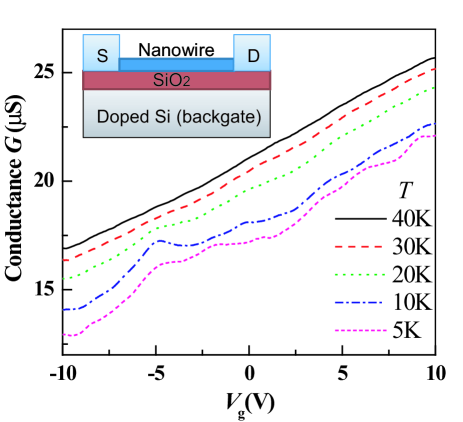
The dependence of the InAs nanowire conductance on the gate voltage at various temperatures and zero magnetic field is shown in Fig.1. The inset shows the device configuration. The positive slope of in Fig.1 indicates that the carrier is -type, similar to reports in the literature samuelsonInAs ; WangDLInAs ; LieberInAs ; JaveyInAs ; sakrAPL . In Fig.1, it can be seen that the curves shift downwards as decreases. This reduction of conductance was attributed to the weak localization correction to the Drude conductance instead of a decreasing carrier density effectliangdong . Below 10K, some small amplitude oscillations start to develop on top of the quasi-linear dependence. These oscillations are either due to the quantization of multiple 1D-subbands with different mobility smallSiNW or interference effects of electron waves undergoing multiple reflections inside the nanowire channel SiNWinterference . From the trans-conductance d/d, we can estimate the electron mobility sakrAPL ; dujuan , where is the gate capacitance and =2m is the length of nanowire between the electrodes. We can approximate the with a wire on an infinite plate model and estimate electron mobility 205cm2/Vs. The electron concentration can be roughly estimated as m. The threshold voltage is -45V by linearly extrapolating the curve to zero at =40K when the quantum correction to is small. Thus for the range of gate voltage studied (-10 to +10V), electron concentration ranges from 1.0 to 1.5104/m, or equivalently, 3.1 to 4.8 1019/cm3. For such high electron concentrations, there are many 1D subbands filled, therefore we use the three-dimensional (3D) formula to estimate the electron mean free path 13.1, 14.4 and 15.2nm, for =-10, 0 and +10V. The corresponding 3D Fermi wavelength is 6.5, 5.9 and 5.6nm.
The magneto-conductance of nanowire is presented in Fig.2a for both the perpendicular field and parallel field configurations at several temperatures from =40K down to 5K. There are two main qualitative observations regarding the magneto-conductance . , at T, both the perpendicular field () and parallel field () induce a positive magneto-conductance, whose magnitude increases at lower temperature. The positive magneto-conductance in has been explained by the suppression of 1D weak localization by us in an earlier paper liangdong . Above 2T, the conductance of nanowire tends to saturate, due to the complete suppression of weak localization effectliangdong . , at all temperatures, the increment in is always larger than . This difference between the transverse magneto-conductance and the longitudinal magneto-conductance is the main focus of this paper. Below we will show that both effects arise from the same mechanism, namely, magnetic field suppression of 1D weak localization.
Quantum correction to the Drude conductivity in weakly disordered system at low temperatures stems from weak localization, which is constructive quantum interference of time-reversal paths formed by diffusive electrons scattered elastically by impurities or defectsBergmann . Such weak localization effects have been widely observed in various disordered electronic systems and received tremendous research interestsLeeRMP . One key parameter in this process is the phase coherence length of electrons , indicating the characteristic length within which the electron maintains its phase coherence for the interference to take place. Phase coherence can be destroyed by electron-electron and electron-phonon scatterings. Such inelastic scatterings are strengthened by increasing temperature, which leads to the diminishing effect of the weak localization effect at high temperatures. Moreover, magnetic field can be applied to introduce additional phase shifts to the electron waves travelling in time-reversed paths, which suppresses the weak localization and enhances the sample conductance. The dependence of conductance on magnetic field is usually used to extract the . If , the width of system, the localization is regarded as 1D, and the quantum correction to conductance in magnetic field is given by the following equation Altshuler81 ; beenakkertheory :
| (1) |
where =2m is the length of the nanowire, =20nm is the width or diameter of nanowire, and is the classical Drude conductance. The magnetic relaxation length , with as the diffusion constant and as the magnetic relaxation time which depends on the field orientation, strength and wire cross-section shape etc. We first fitted the low field (1T) data in Fig.2a to Eq.1 using Altshuler81 ; beenakkertheory ; note . and are the only two fitting parameters. The fitting curves are indicated by the solid line in Fig.2a, while the fitted phase coherence lengths and the Drude conductance at various temperatures are shown in Fig.2b. The above expression for is applicable in the so-called ’dirty metal’ regime (), and Eq.1 requires (the weak field limit). These requirements are satisfied reasonably for our parameters. As shown in the Fig 2b, , ranging from 41.3nm to 103.6nm, is much larger than the diameter of the nanowire. This justifies the use of 1D weak localization () to fit our data. It is interesting to note that the extracted has some temperature dependence. We believe that this residual -dependence in is due to the electron-electron interaction effects, which also give a correction to the Drude conductancesimmonsSiNW ; lujia . It is well known that, unlike weak localization, electron-electron interaction induced quantum correction to conductance is independent of magnetic field LeeRMP . Thus it will not affect our study of orientation-dependent magneto-conductance.
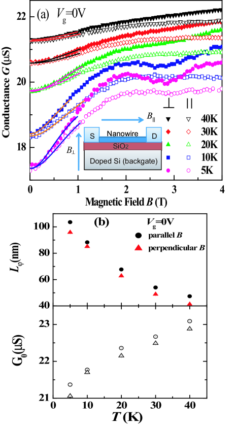
The weak-localization correction to the conductance of a wire in parallel magnetic field was also developed by Altshuler and Aronov Altshuler81 . The analytical expression is the same as Eq.1 but with . We fit the in Fig.2a to Eq.1 using the expression for and found a good agreement. The extracted and are shown in Fig.2b to compare with the results from fitting data. There ia a good agreement. Therefore, both the perpendicular and parallel field induced magneto-conductance are consistent with the localization effect with the same parameters. Before we proceed to the angular dependence of , we like to make a few comments on the physical origin of the stronger in the perpendicular configuration. Evidently, , this means that a perpendicular field is more effective than a parallel field in suppressing the localization effect. This difference is related to the 1D size confinement effect of coherent electron waves (). In the parallel field configuration, electron diffusion paths enclosing magnetic flux are well confined within the circumference of the nanowire, while for the perpendicular field case, they are only confined in the radial direction, and are free of confinement in the axial direction. So the magnetic fluxes enclosed by electron diffusion paths in perpendicular field are larger in the perpendicular field configuration. Thus, the additional phase shift introduced by a small magnetic field for is larger than , which leads to stronger suppression of weak localization effect.
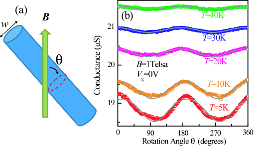
To further test the conclusion that the anisotropic magneto-conductance of our InAs nanowire has the same origin of magnetic field suppression of 1D weak localization, we carried out an angle dependence experiment of the magneto-conductance at various temperatures in a fixed magnetic field of 1T. The nanowire was carefully aligned to make sure it could be rotated about the axis perpendicular to both the magnetic field and the nanowire, as shown in Fig.3a. The rotation angle is defined to be the angle between magnetic field and the cross section plane of nanowire. The experimental data of angle dependence of magneto-conductance for =0 to 360 degrees are given in Fig 3(b). The gate voltage was set to 0V. According to our definition of , is exactly perpendicular to the nanowire at =0 and 180 degrees, and is exactly parallel to nanowire at =90 and 270 degrees. Obviously, since that magneto-conductance in perpendicular field is larger than in parallel field, data in Fig.3b shows peaks at 0, 180 and 360degrees, and dips at 90, 270 degrees. The small deviations of the peak and dip positions from 0, 90, 180 and 270 may be caused by the misalignment of nanowire relative to magnetic field. In addition, the oscillatory amplitudes of decreases as the temperature increases because of the weakening of the weak localization effect at high temperatures. In order to explain the experimental data at an arbitrary angle , we decompose the magnetic field to a perpendicular component and a parallel component. These two orthogonal magnetic fields will both contribute to the suppression of electron localization in nanowire, but with different magnitudes, as discussed earlier. The overall magneto-conductance is then given by
| (2) |
In Eq.2, and are the magnetic relaxation lengths for the perpendicular and parallel components of . The solid curves in Fig 3(b) indicate the theoretical fits to Eq.2, with fixed at the averaged values of data in Fig.2b, and a misalignment angle offset was set as the only free parameter. The fitted angle offset is within 10 degrees. This good agreement between data and theory further supports that the anisotropic magneto-conductance of nanowire is consistently explained by the 1D weak localization theory.
In conclusion, angle dependence of the anisotropic magneto-conductance of a single InAs nanowire with 20nm diameter is studied. The data are consistent with the theory of orientation-dependent suppression of 1D weak localization by a magnetic field Altshuler81 ; beenakkertheory . Not only will the results benefit the fundamental understandings of magneto-transport in nanowires, the continuously tuned angle-dependent magneto-conductance may open up opportunities to explore other delicate effects such as different spin-orbit couplings in semiconductor nanowiresNitta2008 ; Spincontrol09 .
The authors thank L. Qiu and M. MacDonald for useful discussions. X.P.A.G. acknowledges CWRU startup fund and ACS Petroleum Research Fund (Grant 48800-DNI10) for supporting this work.
References
- (1) W. Lu, and C. M. Lieber, Nature Mater. 6, 841 (2007).
- (2) C. Thelander et al., Materials Today 9, 28 (2006).
- (3) W. Lu, J. Xiang, B.P. Timko, Y. Wu and C.M. Lieber Proc. Natl. Acad. Sci. USA 102, 10046 (2005).
- (4) S. R. Rustagi et al., IEEE Elec. Dev. Lett. 28, 909 (2007).
- (5) M.T. Bjork, C. Thelander, A.E. Hansen et al., Nano Lett. 4, 1621 (2004).
- (6) J. Xiang, A. Vidan, M. Tinkham, R.M. Westervelt and C.M. Lieber, Nature Nanotech. 1, 208 (2006).
- (7) Y. Hu, H.O.H. Churchill, D.J. Reilly, J. Xiang, C.M. Lieber and C.M. Marcus, Nature Nanotech. 2, 622 (2007).
- (8) C. Fasth, A. Fuhrer, L. Samuelson, V.N. Golovach, D. Loss, Phys. Rev. Lett. 98, 266801 (2007).
- (9) S. Roddaro et al., Phys. Rev. Lett. 101, 186802 (2008).
- (10) F. A. Zwanenburg, C.E.W.M. van Rijmenam, Y. Fang, C.M. Lieber, and L.P. Kouwenhoven Nano Lett. 9, 1071 (2009).
- (11) M.H.M. van Weert et al., Nano Lett. 9, 1989 (2009).
- (12) L.D. Hicks, M.S. Dresselhaus, Phys. Rev. B 47, 16631 (1993).
- (13) A.I. Hochbaum et al., Nature 451, 163 (2008).
- (14) A. I. Boukai et al., Nature 451 168 (2008).
- (15) A.T. Tilke, F.C. Simmel, H. Lorenz, R.H. Blick, and J.P. Kotthaus Phys. Rev. B 68, 075311 (2003).
- (16) A. E. Hansen, M.T. Bork, C. Fasth, C. Thelander, L. Samuelson, Phys. Rev. B 71, 205328 (2005).
- (17) P. Lehnen, T. Schapers, N. Kaluza, N. Thillosen, H. Hardtdegen, Phys. Rev. B 76, 205307 (2007).
- (18) F. J. Rue, B. Weber, K. E. J. Goh, O. Klochan, A. R. Hamilton, and M. Y. Simmons, Phys. Rev. B 76, 085403 (2007).
- (19) S. Dhara, H.S. Solanki, V. Singh, et al., Phys. Rev. B 79, 121311(R)(2009).
- (20) D. Liang, M. R. Sakr and X.P.A. Gao, Nano Lett. 9, 1709 (2009).
- (21) J. Heremans et al., Phys. Rev. B 58, R10091 (1998).
- (22) R.S. Thompson, D. Li, C.M. Witte, J.G. Lu, preprint arXiv:0907.5282.
- (23) B.L. Altshuler, A.G. Aronov, JETP Lett. 33, 449 (1981).
- (24) C.W.J. Beenakker, H. van Houten, Phys. Rev. B 38, 3232 (1988).
- (25) T. Bryllert, L.E. Wernersson, L.E. Froberg, L. Samuelson, IEEE Electron Dev. Lett. 27, 323 (2006).
- (26) S.A. Dayeh, D. P. R. Aplin, X. T. Zhou, P. K. L. Yu, E. T. Yu, D. L. Wang, Small 3, 326 (2007).
- (27) X. Jiang, Q. Xiong, S. Nam, F. Qian, Y. Li, and C. M. Lieber, Nano Lett. 7, 3214 (2007).
- (28) A. C. Ford, J. C. Ho, Z. Fan, O. Ergen, V. Altoe, S. Aloni, H. Razavi, A. Javey, Nano Research 1, 32 (2008).
- (29) M.R. Sakr, X.P.A. Gao, Appl. Phys. Lett. 93, 203503 (2008).
- (30) J. Du, D. Liang, H. Tang, X.P.A. Gao, Nano Lett. in press (2009).
- (31) G. Bergmann, Phys. Rep. 107, 1 (1984).
- (32) P.A. Lee, T.V. Ramakrishnan, Rev. Mod. Phys. 57, 287(1985).
- (33) Original equation for the perpendicular field configuration was obtained for wires with square cross-section in Ref.Altshuler81 . We modified the equation to account for the circular cross-section of nanowire.
- (34) M. Scheid, M. Kohda, Y. Kunihashi, K. Richter, J. Nitta, Phys. Rev. Lett. 101, 266401 (2008).
- (35) R. G. Nazmitdinov, K. N. Pichugin, M. Valin-Rodriguez, Phys. Rev. B 79, 193303 (2009).