Changes in the electrical transport of ZnO under visible light
Abstract
Complex impedance spectroscopy data in the frequency range 16Hz MHz at room temperature were acquired on pure ZnO single crystal and thin film. The measured impedance of the ZnO samples shows large changes with time after exposure to or covering them from visible light. At fixed times Cole-Cole-diagrams indicate the presence of a single relaxation process. A simple analysis of the impedance data allows us to obtain two main relaxation times. The behavior for both, ZnO crystal and thin film, is similar but the thin film shows shorter relaxation times. The analysis indicates the existence of two different photo-active defects with activation energies between eV and eV.
keywords:
Semiconductors , PhotoconductivityPACS:
78.66.Hf , 72.20.-i1 Introduction
Zinc Oxide (ZnO) is emerging as a material of interest for a variety of electronic applications. It is used in various areas like opto electronics in the blue/ultra-violet range, pharmaceutical industry, UV detectors and as a bio-compatible material [1, 2]. This semiconductor has gained substantial interest in the community in part because of its wide direct band gap ( eV at room temperature [2]). Due its large band gap and small spin orbit coupling, a long spin life time is expected. Therefore, ZnO is a potential candidate for room temperature spintronic applications [3, 5, 6]. Advantages associated with the large band gap include higher breakdown voltages, ability to sustain large electric fields, lower noise generation, and high temperature and high-power operation [2]. Apart from these characteristics it is chemically stable, easy to prepare and nontoxic. Most of the doping materials that are used with ZnO are also readily available.
Although the DC conductivity in pure and doped ZnO samples has received considerable attention in the last years, there have been only a few studies on their AC transport properties. Even though that optical absorption and emission properties of ZnO were already studied recently [6], the effect of visible light on the electrical conductivity has received minor attention. Taking into account that a promising application of ZnO is its use in transparent electronic devices, such as in the fabrication of transparent thin-film transistors [7], it appears advisable to study the electrical impedance of ZnO samples as a function of time after exposure to or covering from visible light. Our results show that for undoped ZnO samples the influence of the photoconductivity to the electrical transport is large and cannot be rejected. Therefore, care should be taken with time-dependent effects on the related properties due to the influence of visible light.
We would like to note that our results obtained only at room temperature provide a guide of the expected changes in the electrical transport in a broad frequency range due to the effect of visible light. This work does not intend to provide a detailed studied on the nature of the defects in pure ZnO crystals and films, a unsolved issue nowadays, but to demonstrate the capability of the used experimental method and the large observed effects in the frequency dependence of the conductivity due to visible light. To the best of our knowledge such a frequency study and the influence of visible light was not yet reported in the literature for ZnO. Studies as a function of the light wavelength and temperature are out of the scope of our work and can be done in the future using a similar experimental method as described here.
2 Experimental Details.
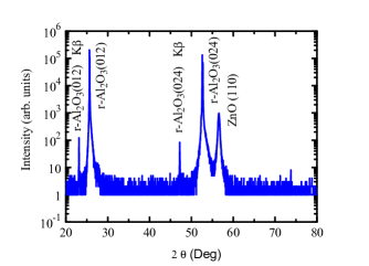
We measured ZnO single crystals obtained from the company Crystec GmbH grown by hydrothermal method and with dimensions mm3. The thin film of 110 nm thickness was prepared by pulsed laser deposition (PLD) on a r-plane sapphire substrate using a substrate temperature of 400 C and oxygen pressure of 0.002 mbar. The grown parameters correspond to the same as those used to produce high-quality thin films by PLD method reported in Ref. [7]. The single phase of the used thin film sample was verified by using X-ray diffraction, which spectra is shown in Fig. 1. The single ZnO peak corresponds to the (1 1 0) plane of the wurtzite structure.
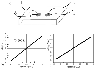
In order to attain high-performance ZnO-based optical and electrical devices it is essential to achieve Ohmic contacts that have both low resistance and are thermally stable and reliable [2]. It is well known that parasitic resistance, in the form of contact resistance, is one of the major obstacles in realizing long-lifetime operation of optical and electrical devices. The major loss of device performance is often caused by high resistance metal-semiconductor contacts through contact failures having potential barriers and/or thermal stress. Four-point probe configuration was used for all electrical measurements in a symmetrical device using gold wires (m diameter) fixed with pure indium on the ZnO surface, as shown schematically in Fig. 2(a). To check for a linear, ohmic behavior of the sample-contact system we have measured the I-V characteristic curves using a Agilent semiconductor analyzer (4155C). Stepwise steady state voltage biased measurements were carried out at room temperature. The obtained I-V curves show a linear and symmetric relationship in a wide range of voltages, see Figs. 2(b) and (c), ensuring that our contacts show Ohmic behavior.
Impedance measurements were carried out using Agilent 4294A impedance analyzer (in the frequency range of 40 Hz to 3 MHz) and a 16 Hz AC resistance LR700 (Linear Research) bridge at room temperature, in dark as well as under visible light (typical luminance lx) as a function of time. We measured the impedance, phase, resistance, and reactance using alternating signals up to 500 mV amplitude. The impedance spectra were obtained as follows: the samples were exposed to visible light for nearly 5 hours until the signal was in a steady state situation (no significant time change) and after a first measurement they were covered. Then, measurements in dark were taken at successive times. All measurements in this work were performed at room temperature in a acclimatized environment (KK).
3 Results
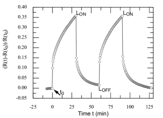
Short time dependent resistance measurements for one of the single crystals are presented in Fig. 3, where we demonstrate the reversibility of the effect of exposure the crystal with light below the ZnO band gap energy and then covering the sample. Other crystals from the same batch show the same behavior. It is remarkable to see that in the first 75 seconds after covering the sample a clear increase in the resistance of the order of 15% is observed, see Fig. 3.
We present below the results of the complex impedance as , where (resistance) and (reactance) are the real and imaginary parts of the impedance. The real part of the impedance versus frequency for the single crystal is shown in Fig. 4(a) where the black curve represents the frequency response of the sample during frequencies. Under light and in dark the real part of the impedance shows a frequency independent region extending from DC to kHz followed by a decrease at higher illumination and in the dark, see Fig. 4(a). The decrease in the real part of the impedance with frequency is in agreement with reported results in the literature [8]. Figure 4(b) shows the variation of the imaginary part of impedance (reactance) with frequency at similar times as in Fig. 4(a). The spectra are characterized by the appearance of a minimum, which shifts to lower frequencies with time. Such behavior indicates the presence of relaxation processes in the system as has been observed in, e.g. Ti-doped LSMO [9].
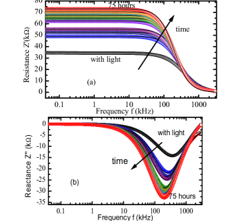
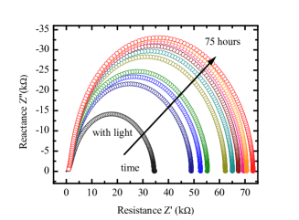
Figure 5 shows the variation of the reactance as a function of the resistance , i.e. Cole-Cole plot, at room temperature at different times after covering the sample. At each time the spectrum appears as a semicircle diagram indicating that a single relaxation mechanism is present [10]. Note the independence of the semicircle diagram from time. Such pattern tells us about the electrical processes occurring within the sample and their correlation with the sample microstructure. In order to analyze the experimental results, a simple equivalent circuit was used to represent the measured system, i.e. a parallel RC circuit connected with an induction L in series. According to this model the expression of the real () and imaginary () components are:
| (1) |
| (2) |
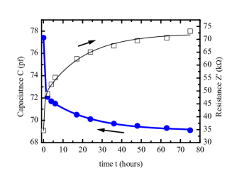
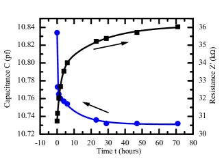
After fitting the experimental curves using the above model, see Fig.4, we have obtained the capacitance for each measurement at a given time. Figure 6 shows the calculated capacitance as a function of time t after covering the sample. We observe that there is an exponential decay of the capacitance with time. This time dependence can be fitted with a combination of two exponential functions: , with and two independent relaxation times and a,b free parameters. From the fit to the data, see Fig. 6, we obtain hours and hours.
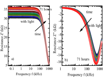
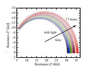
In order to check for the existence of similar effects in thin films we measured the impedance spectra for the ZnO thin film also. Figures 7(a) and 7(b) show the variation of the real and imaginary part of the impedance with frequency when the sample is exposure to and after covering it from visible light. The behavior of these plots is similar to that of the single crystal as well as the Cole-Cole plots, see Fig. 8. Figure 9 shows the capacitance versus time obtained from the fits shown in Fig. 7. Also for the thin film the capacitance decreases exponentially after covering the sample from visible light. The behavior can be fitted with two relaxation times of values 0.1hs and 11hs. These relaxation times are smaller as well as the relative change of the transport properties compared to the values obtained for the single crystal. This result indicates that the structural quality of the samples play a role. From one side a larger defect concentration in the ZnO film compared to the single crystal produces larger scattering then smaller electron mobility. On the other hand the carrier density in the thin film is larger than in the single crystal due to the lattice disorder. These changes due to the structural quality affect the photoconductivity. Similar dependence of the photoconductivity with the microstructure was obtained in TiO2 films [11].
4 Discussion
As pointed out in the introduction a detailed study of the defects that are active in the photoconductivity process of ZnO crystals and films is out of the scope of this work. Neither the nature of the defects nor their behavior under irradiation in this compound is still understood nor does our fixed temperature allow us a detailed study of the activation processes. Therefore we give some general remarks on our results. Let us start with the effects produced by the irradiation of visible light to a semiconductor like ZnO. The time dependent response depends on the corresponding relaxation time of the photon absorption or emission processes [12], processes that are influenced by intrinsic and extrinsic lattice defects. During sub-gap illumination excess carriers are optically excited from localized band gap states and quickly thermalize in the extend states. They will be many times trapped in the localized states and send back to the conduction extended states. After a short time, the shallower state will be in thermal distribution. Eventually, several of them could be trapped in deeper levels and remains frozen. A distribution of shallower traps could be responsible for the short time photoconductivity whereas the slower photoconductivity response could be due to capture of holes in deep trap levels. Which might be the origin of those defect levels? Usually ZnO has n-type character even in the absence of intentional doping. Native defects such as oxygen vacancies or zinc interstitial are often assumed to be the origin of this, but the subject remains controversial [13]. Recent work indicates, for example, the existence of a huge amount of hydrogen () in ZnO single crystals [14]. These impurities can influence the electronic properties of ZnO as has been observed several years ago [15]. On the other hand, in relation to the photoconductivity, it was already suggested that point defects behaving as hole or electron traps, exhibit slow electron-hole recombination [16] compared to other defects.
The behavior obtained for both samples indicates that there should be at least two kinds of photoactive defects in the ZnO samples that are responsible for the behavior of ZnO under visible light. Some of the active defects could be related to the vacancy-hydrogen complexes recently found in ZnO crystals [14]. Also cation and anion vacancies which are double acceptors and donors in ZnO may contribute [17]. Assuming that the processes that contribute to the time dependence we observed are thermally activated, i.e. ) with the activation energy and an attempt frequency, we estimate activation energies = 0.85 eV 0.97eV (0.81 eV 0.93 eV) and 0.95 eV - 1.07 eV (0.93 eV - 1.05 eV) for the short - large relaxation times and assuming as attempt frequencies and for the single crystal (thin film), respectively. These energies are comparable to those found in the literature [16]. Future experimental studies should try to measure the photoconductivity at certain wavelengths and at different temperatures for a complete characterization of the photoactive processes and the defects that play a role in this phenomenon.
5 Conclusions
The impedance spectra of ZnO single crystals and a thin film have been obtained after exposure the samples to visible light and after covering them at room temperature and in a broad frequency range. From the measured impedance parameters we obtained two main relaxation times, a short one of less than 1 hour and a long one above 10 hours, after covering the sample. We found a clear difference in the relaxation times between the single crystal and thin film that should be related to the structural quality of the samples. The observed large visible-light dependence in the electrical impedance in a broad frequency range of both investigated samples can be a limitation for real applications.
References
- [1] C. Klingshirn, J. Fallert, R. Hauschild, H. Kalt, J. Phys. Rev. B. 75, 115203 (2007).
- [2] Ü. Özgür, Ya. I. Alivov, C. Liu, A. Teke, M. A. Reshchikov, S. Dogan, V. Avrutin, S.-J. Cho, H. Morko , J. Appl. Phys. 98, 041301, (2005)
- [3] T. Dietl, H. Ohno, F. Matsukura, J. Gibert, and D. Ferrand, J. Science 287, 1019, (2000).
- [4] T. Fukumura, Y. Yamada, H. Toyosaki, T. Hasegawa, H. Koinumac, M. Kawasaki, J. Applied Surface Science 223, 62 (2004)
- [5] V. A. Karpina, V. I. Lazorenko, C. V. Lashkarev, V. D. Dobrowolski, L. I. Kopylova, V. A. Baturin, S. A. Pustovoytov, A. Ju. Karpenko, S. A. Eremin, P. M. Lytvyn, V. P. Ovsyannikov, and E. A. Mazurenko J. Cryst. Res. Technol. 39, 980 (2004)
- [6] P. F. Carcia, R. S. McLean, M. H. Reilly, and G. Nunes, Jr, J. Appl. Phys. Lett. 82, 1117 (2003).
- [7] M. Lorenz, ZnO as transparent electronic material and its application in thin film solar cells, eds. A. Klein and K. Ellmer, (Springer, Berlin 2007), pages 303-357.
- [8] R. Thangavel, V. Sabarinathan, S. Ramasamy and J. Kumar, Materials Letters 61, 4090 (2007)
- [9] H. Rahmouni, M. Nouiri, R. Jemai, N. Kallel, F. Rzigua, A. Selmi, K. Khirouni, and S. Alaya, J. Magn. Magn. Mater. 316, 23 (2007)
- [10] E. Barsoukov and J. R. Macdonald, Impedance Spectroscopy, Wiley-Interscience (2005).
- [11] D. Comedi, S. P. Heluani, M. Villafuerte, R. D. Arce and R. R. Koropecki J. Phys. Condens. Matter 19, 486205 (2007)
- [12] M. Grundmann, The Physics of semiconductors Springer Berlin 2006, pages 475-498.
- [13] D. C. Look, J. W. Hemsky, and J. R. Sizelove, Phys. Rev. Lett. 82, 2552 (1999)
- [14] G. Brauer, W. Anwand, D. Grambole, J. Grenzer, W. Skorupa, Phys. Rev B 79, 115212 (2009)
- [15] G. Heiland and P. Kunstmann, Surface Science 13, 72 (1969)
- [16] K. Moazzami, T. E. Murphy, J. D. Phillips, M. C-K. Cheung and A. N. Cartwright, Semicond. Sci. Technol. 21, 717 (2006)
- [17] B. K. Meyer, H. Alves, D. M. Hofmann, W. Kriegseis, D. Foster, F. Bertram, J. Christen, A. Hoffmann, et al., Phys. Stat. Sol. (b) 241, 231 (2004)