Excitonic switches at 100 K temperatures
Abstract
pacs:
73.63.Hs, 78.67.DePhotonic and optoelectronic devices may offer the opportunity to realize efficient signal processing at speeds higher than in conventional electronic devices. Switches form the building blocks for circuits and fast photonic switches have been realized Liu04 ; Xu05 ; Green07 ; Jiang05 ; LiuJ08 ; Chen08 . Recently, proof of principle of exciton optoelectronic devices was demonstrated High07 ; High08 . Potential advantages of excitonic devices include high operation and interconnection speed, small dimensions, and the opportunity to combine many elements into integrated circuits. Here, we demonstrate experimental proof of principle for the operation of excitonic switching devices at temperatures around 100 K. The devices are based on an AlAs/GaAs coupled quantum well structure and include the exciton optoelectronic transistor (EXOT), the excitonic bridge modulator (EXBM), and the excitonic pinch-off modulator (EXPOM). This is a two orders of magnitude increase in the operation temperature compared to the earlier devices, where operation was demonstrated at 1.5 K High07 ; High08 .
The operation principle of excitonic devices is based on the control of exciton fluxes by electrode voltages High07 ; High08 . The excitonic devices may have photonic or excitonic inputs and outputs. In the former case, photons transform into excitons at the input and excitons transform into photons at the output High07 . In the latter case, excitons arrive to the input from (depart from the output to) another excitonic device High08 . Potential advantages of excitonic devices are briefly discussed below.
High interconnection speed. Efficient signal communication uses photons. Conventional signal processing, however, uses an optically inactive medium, electrons. An interconnection between electronic signal processing and optical communication causes a delay, thus slowing down the operation speed Miller00 . In contrast, excitons form a medium that can be used for signal processing and, at the same time, directly linked to optical communication. Therefore, the delay between signal processing and optical communication is effectively eliminated in excitonic devices. This can provide a significant advantage in applications where the interconnection speed is important. The switching time combined with the interconnection time for the first proof-of-principle excitonic transistor was ns High07 , close to ultrafast photonic modulators.
Compactness and scalability. Photonic devices demonstrate fast operation speeds; however, the achievement of photonic signal modulation by a control gate usually requires large device dimensions that make the creation of compact circuits with many elements challenging Wakita98 . The smallest achieved dimensions for Mach-Zehnder modulators are m Liu04 ; Xu05 ; Green07 ; Jiang05 ; LiuJ08 ; Chen08 . In comparison, excitonic transistors have an architecture and operation principle similar to electronic field effect transistors (FET). Therefore, excitonic circuits can potentially be similarly compact and can include as many elements as electronic circuits. The diffraction limit for the dimensions of excitonic devices is given by the exciton de Broglie wavelength, much smaller than the diffraction limit for the dimensions of photonic devices given by the wavelength of light (the exciton thermal de Broglie wavelength scales with temperature and is nm at room temperature). In the first proof-of-principle excitonic transistor the distance between the source and drain was m High07 (limited by the resolution of the lithography used for the sample processing), considerably smaller than the dimensions of photonic devices. The proof-of-principle for the integration of excitonic transistors into circuits was demonstrated in High08 .
The major challenges for excitonic devices are finite exciton lifetime and finite exciton binding energy. In a regular direct-gap semiconductor, the exciton lifetime is typically less than a nanosecond, allowing the exciton to travel only a small distance before it recombines. This problem is addressed by using indirect excitons composed of electrons and holes in separated layers High07 ; High08 . The lifetime of indirect excitons exceeds by orders of magnitude the lifetime of regular excitons and increases exponentially with the separation between the layers and the height of the separating barrier. Within their lifetime, indirect excitons can travel over large distances Hagn95 ; Butov98 ; Larionov00 ; Butov02 ; Voros05 ; Gartner06 ; Ivanov06 , for which devices can be readily patterned.
A finite exciton binding energy limits the operation temperature: Excitons exist in the temperature range roughly below Chemla84 ( is the Boltzmann constant). The proof of principle of excitonic devices was done at 1.5 K in a GaAs/Al0.33Ga0.67As coupled quantum well structure (CQW) with nm where K High07 ; High08 . Increasing the operation temperature requires different materials and architectures. The goal is to create efficient excitonic devices that are operational at room temperature. Note that materials with a large include wide-bandgap semiconductors Makino05 and organic materials Segal07 .
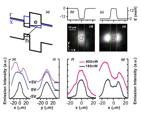
Here, we report on proof of principle for operation of excitonic switches at K. This is a two orders of magnitude increase in the operation temperature compared to the earlier devices, where operation was demonstrated at 1.5 K High07 ; High08 . It shows that the operation of excitonic devices is not limited to liquid Helium temperatures. The devices are based on AlAs/GaAs CQW (Fig. 1a). A small nm results in a high binding energy of indirect excitons in such CQW K Zrenner92 , permitting device operation at elevated temperatures.
We first study exciton transport along and across a m wide electrode. At zero applied voltage , indirect excitons form the lowest energy state in this structure Zrenner92 . Application of a positive (negative) increases (lowers) the exciton energy by ( is the electric field in the z-direction) Miller85 . The linear electrode creates a channel for indirect excitons at negative (Fig. 1b)and anti-channel at positive (Fig. 1c). Figures 1d and 1f show the exciton cloud confinement in the channel. Excitons spread beyond the channel at higher densities (Fig. 1f) due to the screening of the confining potential by the excitons Remeika09 . Figures 1e and 1g show the exciton cloud spreading away from the anti-channel. The exciton emission reaches maximum intensity a few microns away from the anti-channel (the emission profiles in Figs. 1f-i are corrected for the electrode absorption). Both the increased exciton density away from the potential energy hill of the anti-channel and the increased occupation of the optically active exciton states with momenta ( is the bandgap, is the dielectric constant) due to exciton relaxation to states away from the excitation spot at the potential energy hill contribute to the observed intensity increase beyond the anti-channel. The latter mechanism was suggested as an explanation of the exciton rings in Butov02 ; Ivanov06 . Figure 1h shows the transition from a channel to anti-channel with increasing . The confining potential of the channel or potential energy hill of the anti-channel strongly affect the exciton transport in the -direction and relatively weakly affect it in the -direction (Fig. 1h,i). The latter presents the characteristic transport length of indirect excitons in the structure.
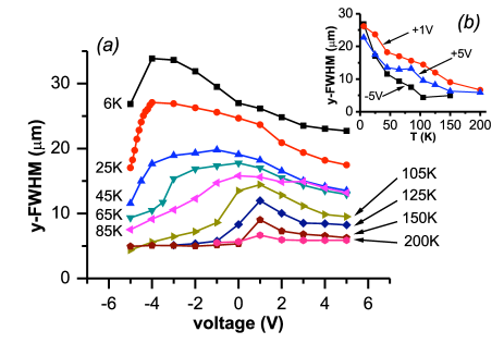
Figure 1 shows that is large enough so that excitons can travel over distances exceeding the dimensions of excitonic devices. reduces with increasing temperature (Fig. 2a,b). At high temperatures, the largest is observed around V (Fig. 2a). These data are consistent with earlier data on exciton lifetime in AlAs/GaAs CQW: reduces (i) at positive due to approaching the direct regime, (ii) at negative due to the escape of electrons and holes from the CQW through the reduced barrier, and (iii) at high temperatures due to increased nonradiative recombination Butov94 ; Butov98 , and the reduction of results in the reduction of ( is the exciton diffusion coefficient).
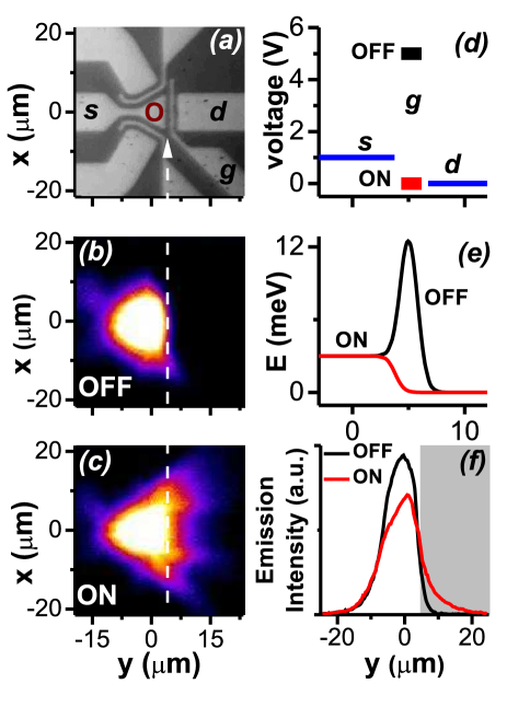
Figure 3 presents the proof of principle for the operation of the exciton optoelectronic transistor (EXOT) at 85 K. The operation principle of the EXOT is similar to that of an electronic FET High07 ; High08 . The EXOT is a three-terminal device in which the exciton flux between two electrodes is controlled by a voltage applied to the third electrode. Here, the EXOT operates in switching mode. The excitons are excited at the source (input) and travel to the drain (output) because of the potential energy gradient created by the source voltage and drain voltage . The exciton flux from source to drain is controlled by a gate voltage , which creates (removes) a barrier in the region of the gate electrode when the EXOT is off (on), see Fig. 3d,e. The emission images for the EXOT in both the off state and on state are shown in Fig. 3b,c. The on/off ratio of the signal integrated over EXOT output (shaded region) reaches 5 (Fig. 3f).
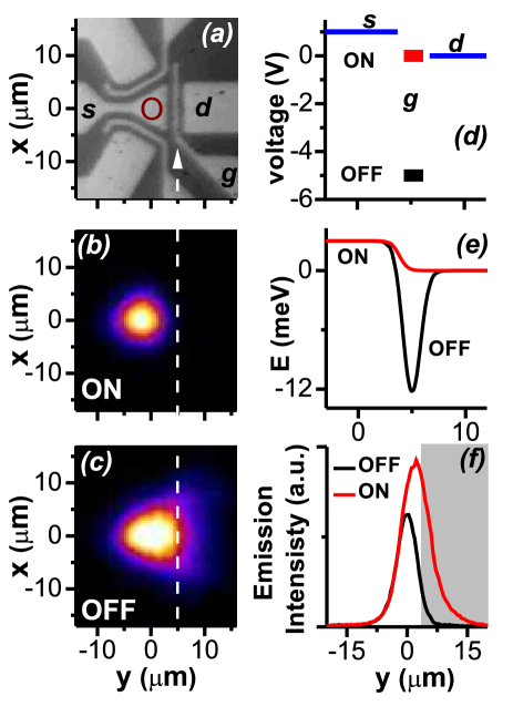
Exciton flux modulations can also be achieved by other configurations of electrode voltages. Figure 4 presents the proof of principle for the operation of the excitonic bridge modulator (EXBM) at 125 K. In this device, the exciton flux from source to drain is terminated in the off state by a considerable reduction of the exciton lifetime in the gate region. This is achieved by applying a large negative voltage on the gate electrode, which increases the carrier escape out of the CQW in the -direction in the gate region Butov94 . In turn, the exciton flux can flow from source to drain when the gate electrode provides a bridge between the source and drain with a long exciton lifetime. The on/off ratio of the signal integrated over EXBM output (shaded region) reaches 9 (Fig. 4f).
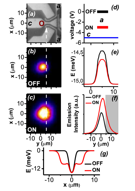
Figure 5 presents the proof of principle for the operation of the excitonic pinch-off modulator (EXPOM) at 85 K. In this device, the exciton flux through the m constriction in the electrode – the channel – is controlled by varying the voltage on the laterally adjacent electrodes . Increasing narrows the channel and also increases the exciton energy in the channel (Fig. 5e,g), reducing the exciton flux through it. The EXPOM is similar to split gate electronic devices. The on/off ratio of the signal integrated over the area right of the channel (shaded region) reaches 12 (Fig. 5f).
At high temperatures K, the exciton transport length becomes small compared to the device dimensions (Fig. 2), become comparable to the temperature, and the on/off ratio for the switches in the AlAs/GaAs CQW vanishes. The optimization of excitonic devices is the subject of on-going research.
This work is supported by ARO and NSF.
Methods The structure was grown by molecular beam epitaxy. An -GaAs layer with cm-3 serves as a homogeneous bottom electrode. The top electrodes were fabricated by depositing a semitransparent layer of Ti (2 nm) and Pt (8 nm). The 2.5 nm GaAs QW and 4 nm AlAs QW were positioned m above the -GaAs layer within an undoped m thick Al0.45Ga0.55As layer. Positioning the CQW closer to the homogeneous electrode suppresses the in-plane electric field Hammack06 , which otherwise can lead to exciton dissociation. Excitons were photoexcited by a 633 nm HeNe laser within a m FWHM (full width at half maximum) spot. The emission images were taken by a CCD with an interference filter covering the spectral range of the indirect excitons emitting in the vicinity of 690 nm or using a spectrometer with resolution 0.4 meV. The spatial resolution was m. The single-exciton energy profiles were estimated as in Hammack06 .
References
- (1) Liu, A., Jones, R., Liao, L., Samara-Rubio, D., Rubin, D., Cohen, O., Nicolaescu, R., Paniccia, M. A high-speed silicon optical modulator based on a metal-oxide-semiconductor capacitor. Nature 427, 615-618 (2004).
- (2) Xu, Q., Schmidt, B., Pradhan, S., Lipson, M. Micrometre-scale silicon electro-optic modulator. Nature 435, 325-327 (2005).
- (3) Jiang, Y., Jiang, W., Gu, L., Chen, X. Chen,R.T. 80-micron interaction length silicon photonic crystal waveguide modulator. Appl. Phys. Lett. 87, 221105 (2005).
- (4) Green, W. M. J., Rooks, M. J., Seekaric, L., Vlasov Y.A. Ultra-compact, low RF power, 10 Gb/s silicon Mach-Zehnder modulator. Opt. Express 15, 17106-17113 (2007).
- (5) Liu, J., Beals, M., Pomerene, A., Bernardis, S., Sun, R., Cheng, J., Kimerling, L.C., Michel, J. Waveguide-integrated, ultralow-energy GeSi electro-absorption modulators. Nature Photonics 2, 433-437 (2008).
- (6) Chen, H.W., Kuo, Y.H., Bowers, J.E. High speed hybrid silicon evanescent Mach-Zehnder modulator and switch. Opt. Express 16, 20571-20576 (2008).
- (7) High, A.A., Hammack, A.T., Butov, L.V., Hanson, M., Gossard, A.C. Exciton optoelectronic transistor. Optics Lett. 32, 2466-2468 (2007).
- (8) High, A.A., Novitskaya, E.E., Butov, L.V., Hanson, M., Gossard, A.C. , Control of Exciton Fluxes in an Excitonic Integrated Circuit. Science 321, 229-231 (2008).
- (9) Miller, D.A.B. Rationale and Challenges for Optical Interconnects to Electronic Chips. IEEE 88, 728-749 (2000)
- (10) Wakita, K. Semiconductor Optical Modulators (Kluwer Academic Publishers, Norwell, MA, 1998).
- (11) Hagn, M., Zrenner, A., Böhm, G., Weimann G. Electric-field-induced exciton transport in coupled quantum well structures. Appl. Phys. Lett. 67, 232-234 (1995).
- (12) Butov, L.V., Filin, A.I. Anomalous transport and luminescence of indirect excitons in AlAs/GaAs coupled quantum wells as evidence for exciton condensation. Phys. Rev. B 58, 1980-2000 (1998).
- (13) Larionov, A.V., Timofeev, V.B., Hvam, J., Soerensen, K. Interwell excitons in GaAs/AlGaAs double quantum wells and their collective properties. Sov. Phys. JETP 90, 1093-1104 (2000).
- (14) Butov, L.V., Gossard, A.C., Chemla, D.S. Macroscopically ordered state in an exciton system. Nature 418, 751-754 (2002).
- (15) Vörös, Z., Balili, R., Snoke, D.W., Pfeiffer, L., West, K. Long-Distance Diffusion of Excitons in Double Quantum Well Structures. Phys. Rev. Lett. 94, 226401-226404 (2005).
- (16) Gartner, A., Holleithner, A.W., Kotthaus, J.P., Schul, D. Drift mobility of long-living excitons in coupled GaAs quantum wells. Appl. Phys. Lett. 89, 052108 (2006).
- (17) Ivanov, A.L., Smallwood, L.E., Hammack, A.T., Sen Yang, Butov, L.V., Gossard, A.C. Origin of the inner ring in photoluminescence patterns of quantum well excitons. Europhys. Lett. 73, 920-926 (2006).
- (18) Chemla, D.S., Miller, D.A.B., Smith, P.W., Gossard, A.C., Wiegmann, W. Room temperature excitonic nonlinear absorption and refraction in GaAs/AlGaAs multiple quantum well structures. IEEE J. Quantum Electron. 20, 265-275 (1984).
- (19) Makino, T., Segawa, Y., Kawasaki, M., Koinuma, H. Optical properties of excitons in ZnO-based quantum well heterostructures. Semicond. Sci. Technol. 20, S78-S91 (2005).
- (20) Segal, M., Singh, M., Rivoire, K., Difley, S., Van Voorhis, T., Baldo, M.A. Extrafluorescent electroluminescence in organic light-emitting devices. Nature Materials 6, 374-378 (2007).
- (21) Zrenner, A. Festkörperprobleme/Advances in Solid State Physics. Vol. 32,p. 61 (Vieweg, Braunschweig, 1992).
- (22) Hammack, A.T., Gippius, N.A., Sen Yang, Andreev, G.O., Butov, L.V., Hanson, M., Gossard, A.C. Excitons in electrostatic traps. J. Appl. Phys. 99, 066104 (2006).
- (23) Miller, D.A.B., Chemla, D.S., Damen, T.C., Gossard, A.C., Wiegmann, W., Wood, T.H., Burrus, C.A. Electric field dependence of optical absorption near the band gap of quantum-well structures. Phys. Rev. B 32, 1043-1060 (1985).
- (24) Remeika, M., Graves, J.C., Hammack, A.T., Meyertholen, A.D., Fogler, M.M., Butov, L.V., Hanson, M., Gossard, A.C. Localization-Delocalization Transition of Indirect Excitons in Lateral Electrostatic Lattices. Phys. Rev. Lett. 102, 186803 (2009).
- (25) Butov, L.V., Zrenner, A., Abstreiter, G., Böhm, G., Weimann, G. Condensation of indirect excitons in coupled AlAs/GaAs quantum wells. Phys. Rev. Lett. 73, 304-307 (1994).