Conductance properties of rough quantum wires with colored surface disorder
Abstract
Effects of correlated disorder on wave localization have attracted considerable interest. Motivated by the importance of studies of quantum transport in rough nanowires, here we examine how colored surface roughness impacts the conductance of two-dimensional quantum waveguides, using direct scattering calculations based on the reaction matrix approach. The computational results are analyzed in connection with a theoretical relation between the localization length and the structure factor of correlated disorder. We also examine and discuss several cases that have not been treated theoretically or are beyond the validity regime of available theories. Results indicate that conductance properties of quantum wires are controllable via colored surface disorder.
pacs:
73.20.Fz, 73.63.Nm, 73.23.-b, 73.21.HbI Introduction
Ever since Anderson’s model of electron transport in disordered crystals Anderson , wave localization in disordered media has attracted great interests due to their universality. For example, two recent experiments directly observed matter-wave localization in disordered optical potentials using Bose-Einstein condensates BECexp1 ; BECexp2 . One of the most known results from Anderson’s model is that in one-dimensional (1D) disordered systems, the electron wavefunction is always exponentially localized and hence does not contribute to conductance for any given strength of disorder. Note however, this seminal result is based on the strong assumption that the disorder is of the white noise type. If the disorder is colored due to long-range correlations, then a mobility edge may occur in one-dimensional systems as well izprl .
Quantum transport in nanowires is of great interest due to their potential applications in nanotechnology. In addition to the possibility of ballistic electron transport, quantum nanowires are found to show many other important properties. In particular, silicon nanowires can have better electronic response time Ramayya as well as desirable thermoelectric properties thermo . It is hence important to ask how the nature of surface disorder of quantum wires, modeled by quantum waveguides in this study, affects their conductance properties.
Remarkably, if the surface scattering contribution is weak, then it is possible to map the conduction problem of a long two-dimensional (2D) rough waveguide to that of a 1D Anderson model of localization, with the disorder potential determined by the surface roughness firsttime ; freilikher . Initially this mapping was established for one-mode scattering but later it was generalized for any number of modes in the transverse direction izoptic . As such, a quantum wire with white-noise surface disorder will have zero conductance if the localization length is much smaller than the wire length. However, in reality the surface disorder of a rough quantum wire always contains correlations. As a result it becomes interesting and necessary to understand the conductance properties in rough quantum wires with their surface disorder modeled by colored noise. This has motivated several pioneering theoretical studies firsttime ; freilikher ; izoptic ; izprl ; Alberto ; Bagci . Under certain approximations the theoretical studies predicted localization-delocalization transitions of electrons in 2D waveguides with colored surface disorder. Some theoretical details were tested by examining the eigenstates of a closed system with rough boundaries iznum . Moreover, the predicted mobility edge due to colored disorder was recently confirmed in a microwave experiment Kuhl .
Using a reaction matrix formalism for direct scattering calculations, here we computationally study the conductance properties of rough quantum wires with colored surface disorder. The motivation is threefold. First, though the dependence of the localization length upon the correlation function of surface roughness is now available from theory, how the more measurable quantity, namely, the conductance of the waveguide, depends on colored surface roughness has not been directly examined. This issue can be quite complicated when the localization length becomes comparable to the waveguide length. Second, computationally speaking it is possible to consider any kind of colored surface disorder, thus realizing interesting circumstances that are not readily testable in today’s experiments. Indeed, in our computational study we can create rather arbitrary structures in the surface disorder correlation function and then examine the associated conductance properties. Third, direct computational studies allow us to predict some interesting conductance properties that have not been treated theoretically or go beyond the validity regime of available theories firsttime ; freilikher ; izoptic ; izprl ; izprb . For example, we shall study the conductance properties for very strong surface roughness, for rough bended waveguides, and for scattering energies that are close to a shifted threshold value for transmission. The long-term goal of our computational efforts would be to explore the usefulness of colored surface disorder in controlling the conductance properties.
This paper is organized as follows. In Sec. II we describe the scattering model of a quantum wire with colored surface disorder. Therein we shall also briefly introduce the methodology we adopt for the scattering calculations. In Sec. III we present detailed conductance results in a variety of one-mode scattering cases and discuss these results in connection with theory. Concluding remarks are made in Sec. IV.
II Quantum scattering in waveguides with colored surface disorder
II.1 Modeling waveguides with colored surface disorder
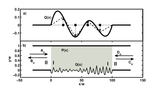
We treat quantum wires as a long 2D waveguide as illustrated in Fig. 1(b). The scattering coordinate is denoted and the transverse coordinate is denoted . The width of the waveguide is denoted and the length is denoted . In all the calculations and is set to be unity. That is, we scale all length by the waveguide width. The upper and lower boundaries of the waveguide are described by and . The case in Fig. 1(b) represents a situation where the upper boundary is a straight line () and the lower boundary is rough. As in our other studies of rough waveguides akgucprb06 ; akgucprb08 , we form a rough waveguide boundary in three steps. First, we divide a rectangular waveguide into pieces of equal length . Second, the end of each piece is shifted in randomly, with the random -displacement, denoted , satisfying a Gaussian distribution. Third, we use spline interpolation to combine those sharp edges to generate a smooth curve for either the upper or the lower waveguide boundary. For the sake of clarity, Fig. 1(a) depicts this procedure with the number of random shifts being as small as . In all our calculations below we set . In Fig. 2(a) we show one realization of the surface roughness function .
The function may be characterized by its ensemble-averaged mean and its self-correlation function , i.e.,
| (1) |
where is the variance of . In the limit of white noise roughness, is proportional to . But more typically, decays at a characteristic length scale, called the correlation radius . For our case here, because the randomness is introduced after dividing the waveguide into pieces, the correlation length of the we construct here is of the order of . This length scale is comparable to the wavelength of the scattering electrons in the one-mode regime.
One tends to characterize the strength of the surface roughness by the variance defined above. However, in practice it is better to use the maximal absolute value of , denoted , to characterize the roughness strength. This is because for strong roughness with a given variance, there is a possibility that some of the random displacements become too large such that the waveguide may be completely blocked. Recognizing this issue, we first set a value of and then, after having generated a roughness function based on spline interpolation, rescale such that its maximal absolute value is given by .
The roughness function obtained above does not have any peculiar features. There are a number of ways to introduce some structure to the correlation function . In Ref. generator a filtering function method was proposed to produce a power-law decay of from white noise. Here we adopt the approach used in Ref. oldexp , which is based on the convolution theorem of Fourier transformations. In particular, the discrete form of autocorrelation function of is defined as
| (2) |
where , is the total number of grid points along , and is a normalization constant such that corr-note . In Fig. 2(b) we show the autocorrelation function for the surface roughness function depicted in Fig. 2(a). The autocorrelation drops from its peak value to near zero at a scale of , which is much smaller than the waveguide length.

As will be made clear in what follows, it is important to consider the Fourier transform of , i.e., the autocorrelation function in the Fourier space. This important quantity is denoted , where is the wavevector conjugate to . Using the Fast Fourier transform of , can be evaluated as follows:
| (3) |
where the value of on the left side is determined by the value of on the right side via . In our calculations we choose . Note that is a real function due to the evenness of . The real function is called below the structure factor of the surface roughness. Figure 2(c) shows the structure factor obtained from the correlation function shown in Fig. 2(b).
Additional correlations in the surface disorder can now be generated by modulating the structure factor . Because the structure factor for a single realization is equivalent to the square of the Fourier transform of , we may imprint interesting structures onto by convoluting with some filtering function. Consider then the function with . Its Fourier transform is a step function of , izoptic with a height and the step edge located at . Consider then a combination of such functions, i.e.,
| (4) |
where , , are predefined parameters. Then the Fourier transform will be if or ; and zero otherwise. If we now consider the following roughness function maxnote ,
| (5) |
then according to the convolution theorem, we have
| (6) |
where is the structure factor for the new surface roughness function . As such, the structure of is directly imprinted on . That is, computationally speaking, arbitrary modulation can be imposed on the structure factor by filtering out the unwanted components and magnifying other desired structure components. Below we apply this simple technique to create different kinds of surface roughness correlation windows and then examine the conductance properties. In Fig. 2(d) we show one example of . Its Fourier transform amplitude, as shown in Fig. 2(e), displays two windows. As shown in Fig. 2(f), this double-window structure is passed to due to Eq. (6). Finally, in Fig. 2(g) we show the surface roughness function , which obviously contains more correlations than the old surface roughness function shown in Fig. 2(a).
II.2 Reaction matrix and scattering matrix
Here we briefly describe how we calculate the electron conductance of a rough 2D waveguide as described above. The Hamiltonian for the quantum transport problem is given by
| (7) |
where is the electron effective mass and represents a hard wall confinement potential. That is, is zero in and becomes infinite otherwise. In our early work akgucprb06 ; akgucprb08 we formulated such a waveguide scattering problem in detail in terms of the so-called reaction matrix method. In the reaction matrix method we first expand scattering state in the scattering region (region I, gray area in Fig. 1(b)) in terms of a complete set of basis states. The basis states are obtained by transforming the rough waveguide into a rectangular one, with the expense of a transformed Hamiltonian with extra surface dependent terms. The solutions in the leads (region II, Fig. 1(b)) are given by
| (8) |
for the left and right leads, respectively. Here is the index for the modes in the transverse direction, and the wavevector is given by
| (9) |
where is the initial electron energy. The scattering coefficients , , and in Eq. (8) are determined by the scattering matrix , which relates the outgoing states to the incoming states. Specifically,
| (10) |
where the submatrices and denote the reflection matrix and and denote the transmission matrix. In the case of one-mode scattering () considered below, will be simply denoted as , with . The matrix is related to the so-called -matrix in the reaction matrix method as follows,
| (11) |
where is maximal number of propagating modes and is a unit matrix, and is diagonal matrix with diagonal elements determined by the wavevector associated with each scattering channel akgucprb06 ; akgucprb08 . Once the matrix is obtained from the matrix, the conductance is calculated by , where is the conductance quanta. Note that in our calculations we include about 10 evanescent modes though we focus on the energy regime where only one mode in the -direction admits propagation along . As to the number of basis states we use in describing the transformed rectangular waveguide, we use 1000 basis states for the degree of freedom and basis states for the degree of freedom. Such a large number of basis states is for a good description of the scattering wave function inside the waveguide, and this number should not be confused with the number of propagating modes or evanescent. Good convergence is obtained in our calculations. Note also that due to the large number of basis states used in the scattering direction, the Fourier transform techniques developed in Ref. akgucprb06 is especially helpful.
III Effects of Colored Surface Disorder On Conductance
With the mapping between the scattering problem in 2D waveguide and 1D Anderson’s model firsttime ; freilikher , early theoretical work firsttime ; izoptic established that the localization length of the 2D waveguide problem is given by
| (12) |
where is either the structure factor or the new structure factor after a convolution procedure. If , a transmitting state is expected and if , then the electron can only make an exponentially small contribution to the conductance. As such, one expects transmitting states when the structure factor is essentially zero; and negligible conductance if is significant and if is not too small. This suggests that the conductance properties can be manipulated by realizing different surface roughness functions.
Equation (12) is obtained under a weak electron scattering approximation (Born approximation). As such, the theoretical result of Eq. (12) may not be valid if is not small as compared with or if the scattering electron is close to the threshold value of channel opening. Another assumption in the theory is that should be much greater than , the radius of the surface correlation function .
III.1 Straight Rough Waveguides
However, in our computational studies we will examine some interesting cases that are evidently beyond the validity regime of the theory. For example, the strength of the surface disorder may not be small and the scattering energy may be placed in the vicinity of a shifted channel opening energy.
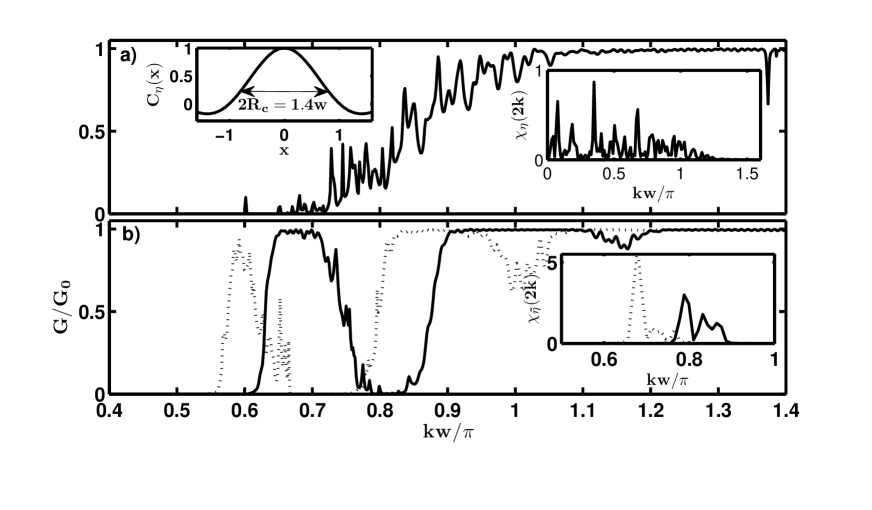
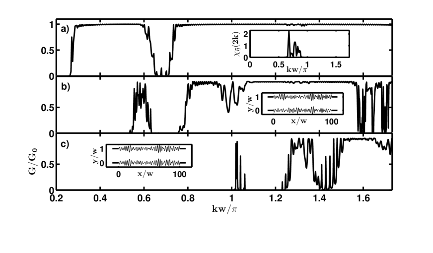
In Fig. 3(a) we show conductance results averaged over three realizations of a rough waveguide, with a flat upper boundary and a rough lower boundary . The strength of the surface disorder is characterized by . Due to our procedure in generating a fixed , the variance of the surface function in each single realization of the surface function will change slightly. For the three realizations used in Fig. 3(a), , and . As is clear from Fig. 3(a), there exists a threshold beyond which the system becomes transmitting (this threshold will be explained below). In the transmission regime the conductance shows a systematic trend of increase as the wavevector increases. The inset of Fig. 3(a) shows , one key term in Eq. (12). The characteristic magnitude of for the shown regime of is . Using Eq. (12), one obtains that the localization length is comparable to . This prediction is hence consistent with our computational results that demonstrate considerable transmission.
Next we exploit the convolution technique described above to form new rough surfaces described by . In particular, the inset of Fig. 3(b) shows two sample cases with distinctively different surface structure factors. In one case (dotted line) has significant values in the interval . Indeed, during that regime the value of is many times larger than the mean value of in the case of Fig. 3(a). In the other case (solid line) is large only in the regime of . For these regimes, the theory predicts that the localization length to be much smaller than the waveguide length and hence vanishing conductance. This is indeed what we observe in our computational study. As shown in Fig. 3(b), either the dotted or the solid conductance curve display a sharp dip in a regime that matches the main profile of .
In addition, similar to what is observed in Fig. 3(a), Fig. 3(b) also displays a transmission threshold. Take the dotted line in Fig. 3(b) as an example. For , there is no transmission at all, even though in that regime is essentially zero. This suggests that this threshold behavior is unrelated to surface roughness details. Rather, it can be considered as a non-perturbative result that is not captured by Eq. (12). To qualitatively explain the observed threshold, we realize that due to the relatively strong surface roughness, the effective width of the waveguide decreases and as a result, the effective mode opening energy increases akgucprb06 . For , we estimate that the effective width of the waveguide is given by . Hence, the corrected mode opening energy is now given by . Using Eq. (9), this estimate gives that, regardless of the surface roughness details, the threshold value for transmission is , which is close to what is observed in Fig. 3. Such an explanation is further confirmed below. This also demonstrates that the maximal value of is an important quantity to characterize the surface roughness strength. Of course, the exact dependence of the effective waveguide width upon is beyond the scope of this work kro .
The results in Fig. 3 show that even when the surface roughness is strong enough to significantly shift the threshold energy for transmission, the surface structure factor may still be well imprinted on the conductance curve. Moreover, the resultant windows of the conductance curves in Fig. 3 are seen to match the location of the structure factor peak. Nevertheless, one wonders how such an agreement might change if we tune the strength of the surface roughness.
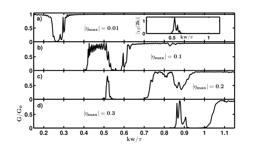
To that end we examine in Fig. 4 four scattering cases with increasing roughness strength, with and in Fig. 4(a) (representing a case with quite weak surface roughness), and in Fig. 4(b), and in Fig. 4(c), and and in Fig. 4(d) (representing a case with very strong surface roughness). The main profile of the structure factor is also shifted closer to the threshold regime observed in Fig. 3. For the case with , the theory based on the weak roughness assumption is not expected to hold. Indeed, In Fig. 4(d) the transmission threshold is right shifted further to the high energy regime as compared with those seen in Fig. 3 or other panels in Fig. 4. Nevertheless, we still observe a clear window of almost zero conductance, but now with its location also significantly shifted as compared with the profile of . For the case of in Fig. 4(c), it is somewhat similar to the dotted line in Fig. 3(b), consistent with the fact that they have the same roughness strength. However, because here the location of the peak of is close to the threshold value, the zero conductance window is also near this threshold: the conductance curve rises when exceeds the threshold and then it quickly drops to zero again. For the case of , its zero conductance window shown in Fig. 4(b) is narrower than those in Fig. 4(c) and Fig. 4(d), consistent with our intuition. Somewhat surprising is the case shown in Fig. 4(a), where the roughness strength is weak and the energy threshold for transmission is almost unaffected. But still, a narrow window for very small conductance is clearly seen in Fig. 4(a). This result is unexpected, because if one applies Eq. (12) directly, one would predict that no such conductance window should occur for . Further, the conductance window in Fig. 4(a) is much left-shifted as compared with the profile of (inset of Fig. 4(a)). Similar results are obtained in other realizations of the surface roughness function that have similar profile of the structure factor smallknote . Such a remarkable deviation from the theory, we believe, is due to a breakdown of the Born approximation in deriving Eq. (12). Indeed, the conductance window for is located in a regime of very low scattering energy, and is hence not describable by a theory based on the Born approximation. Certainly, it should be of considerable interest to experimentally study the conductance windows in these cases of weak surface roughness.
To further confirm that the conductance windows observed here are due to the colored surface disorder, we note that if we consider a surface function as that shown in the inset of Fig. 3(a), then all the conductance windows shown here indeed disappear and the results will become similar to what is shown in Fig. 3(a).
III.2 Bended Rough Waveguides
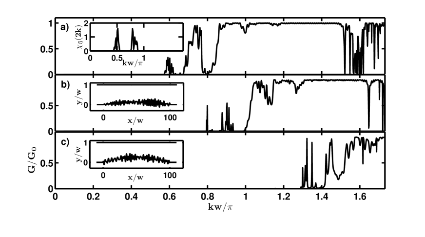
In Fig. 5 we examine the conductance properties of a bended rough waveguide (Fig. 5(b) and Fig. 5(c)) as compared with those of a straight rough waveguide (Fig. 5(a)). In all the three cases shown in Fig. 5, the upper boundary is given by ; and the lower boundary is a parabolic curve plus random fluctuations, i.e., ; with in Fig. 5(a), in Fig. 5(b), and in Fig. 5(c). As to the structure factor of , it is assumed to be of a double-window form as shown in the inset of Fig. 5(a), with the same as in Fig. 3. In the case of a straight rough waveguide, this double-window structure factor creates an analogous double-window structure in the conductance curve (Fig. 5(a)), with its location matching the profile of the structure factor. Interestingly, as we introduce a curvature in the lower boundary in Fig. 5(b), the double-window structure survives but shifts considerably toward higher values. In Fig. 5(c), the curvature of the rough waveguide further increases, the transmission threshold value of also increases (as expected), and the fingerprints of the double-window structure factor can still be seen in the conductance curve. We have also checked if we create three windows in the structure factor, then three windows in the conductance curves can be induced as well, with their locations controllable by tuning the curvature of the bended waveguide.
Finally we consider waveguides with both upper and lower boundaries being rough. Interestingly, in this case a more sophisticated theory izprb shows that the scattering can be regarded as the scattering in a smooth waveguide plus an additional effective potential. The theoretical electron mean free path, calculated using a Green function averaged over different surfaces, is shown to be contributed by different terms, due to different mechanisms called amplitude scattering, gradient scattering, and square gradient scattering izprb . The importance of these terms depends on whether the upper and lower boundaries are symmetric, uncorrelated or anti-symmetric. Motivated by this interesting prediction, here we show in Fig. 6 three computational results, for symmetric (Fig. 6(a)), uncorrelated (Fig. 6(b)), and anti-symmetric boundaries (Fig. 6(c)), all with the same roughness strength as in Fig. 3.
For the symmetric case, the effective waveguide width is not affected by the roughness. By contrast, for the antisymmetric case of Fig. 3(c), the effective waveguide width is most affected. These two simple observations explain why the threshold value for transmission is the smallest in Fig. 6(a) and the largest in Fig. 6(c). Even more noteworthy is how the structure factor of surface roughness generates a conductance window for these three cases. In particular, the window of the conductance drop in the symmetric case (Fig. 6(a)) is narrower than that seen in Fig. 6(b) and Fig. 6(c). Moreover, the conductance window in the anti-symmetric case is the widest one, and is much shifted towards high values as compared with the structure factor. This large mismatch between the conductance window and the peak location of hence reflects clearly an effect from the correlation between the two rough boundaries. Though our results cannot be easily explained by the theoretical result of Eq. (12), they are consistent with the theoretical prediction in Ref. izprb that among the three cases of symmetric, uncorrelated and anti-symmetric waveguides, the electron mean free path in anti-symmetric waveguides should be the shortest.
IV Discussion and Conclusion
In this computational study we have focused on how the structure of surface roughness impacts the conductance properties of electrons propagating in a quantum wire modeled by a 2D waveguide. Our conductance results are directly computed from a reaction matrix approach. An early theoretical result is hence confirmed by detailed behavior of the conductance, a quantity that should be measurable in experiments. In addition, our results for symmetric, uncorrelated, and anti-symmetric rough waveguides are consistent with a very recent theory izprb .
Unlike in the bulk case, for quantum wires of limited length the sensitive dependence of the localization length upon the structure factor of surface roughness can be easily manifested in conductance properties. Our direct scattering calculations show that this is true, even for those interesting cases that are beyond the domain of today’s theory or have not been treated theoretically. We conclude that conductance properties are easily controllable by engineering the surface roughness of quantum wires.
Though we have focused on the transport behavior of electrons, we believe that our methodology might be also useful for studies of other types of wave propagation in disordered systems. In particular, there is now a keen interest in understanding phonon transport in rough quantum wires. Recent computational work Murphy and experiment work Li showed the importance of surface disorder in the heat transport of thin silicon nanowires with a radius of nm. It was also demonstrated experimentally that surface roughness can be used to dramatically suppress heat conductivity thermo and hence enhance thermoelectric efficiency for thin silicon nanowires with a radius about nm. Our computational tools, together with the guidance from the theory firsttime ; freilikher ; izoptic ; izprl ; izprb , might help answer some important questions regarding to phonon transport in rough nanowires. Indeed, we conjecture that it should be possible to design some colored surface to create conductance windows for phonons, but not for electrons. If this is indeed realized, then electron conductance is not much affected and phonon conductance will be greatly reduced. This will be of vast importance to thermoelectric applications.
Finally, we note that spin accumulation in quantum waveguides with rough boundaries was recently studied in Ref. akgucprb08 . It should be interesting to see how colored surface disorder might have some useful impact on spin accumulation effects or spin transport.
Acknowledgements.
We thank Prof. Li Baowen for interesting discussions. This work was supported by the start-up fund (WBS grant No. R-144-050-193-101/133), National University of Singapore, and the NUS “YIA” fund (WBS grant No. R-144-000-195-123), from the office of Deputy President (Research & Technology), National University of Singapore. One of the authors, G.B. Akguc, thank F. M. Izrailev for fruitful discussions. We also thank the Supercomputing and Visualization Unit (SVU), the National University of Singapore Computer Center, for use of their computer facilities.References
- (1) P. W. Anderson, Phys. Rev. 109, No. 5, 1492 (1957).
- (2) G. Roati, C. D Errico, L. Fallani, M. Fattori, C. Fort, M. Zaccanti, G. Modugno, M. Modugno, and M. Inguscio, Nature 453, 895 (2008).
- (3) J. Billy, V. Josse, Z. C. Zuo, A. Bernard, B. Hambrecht, P. Lugan, D. Clement, L. Sanchez-Palencia, P. Bouyer, and A. Aspect, Nature 453, 891 (2008).
- (4) F. M. Izrailev and A. A. Krokhin, Phy. Rev. Lett. 82, 4062 (1999).
- (5) E. B. Ramayya, D. Vasileska, S. M. Goodnick, and I. Knezevic, IEEE Transactions On Nanotechnology 6, 1 (2008).
- (6) A. I. Hochbaum, R. K. Chen, R. D. Delgado, W. J. Liang, E. C. Garnett, M. Najarian, A. Majumdar, and P. D. Yang, Nature 451, 163 (2008).
- (7) V. D. Freilikher, N. M. Makarov and I. V. Yurkevich, Phys. Rev. B 41, 8033 (1989).
- (8) V. D. Freilikher, S.A. Gredeskul, J. Opt. Soc. Am. 7, 868 (1990).
- (9) F. M. Izrailev and N. M. Makarov, Optics. Lett. 26, 1604 (2001); F. M. Izrailev and N. M. Makarov, Appl. Phys. Lett. 84, 5150 (2004).
- (10) A. Rodriguez and J. M. Cervero, Phys. Rev. B 74, 104201 (2006).
- (11) V. M. K. Bagci and A. A. Krokhin, Phys. Rev. B 76, 134202 (2007).
- (12) F. M. Izrailev, J. A. M ndez-Berm dez, and G. A. Luna-Acosta, Phys. Rev. E 68, 066201 (2003).
- (13) U. Kuhl, F. M. Izrailev, and A. A. Krokhin, Phys. Rev. Lett. 100, 126402 (2008).
- (14) F. M. Izrailev, N. M. Makarov, M. Rendon, Phys. Rev. B 73, 155421 (2006); M. Rendon, F. M. Izrailev, N. M. Makarov, Phys. Rev. B 73, 205404 (2007).
- (15) G. B. Akguc and T. H. Seligman, Phys. Rev. B 74, 245317 (2006).
- (16) G. B. Akguc and J. B. Gong, Phys. Rev. B 77, 205302 (2008).
- (17) F. M. Izrailev, A. A. Krokhin, N. M. Makarov, and O. V. Usatenko, Phys. Rev. E 76, 027701 (2007).
- (18) U. Kuhl, F. M. Izrailev and A. A. Krokhin, and H.-J. Stockmann, App. Phys. Lett. 77, 633 (2000).
- (19) Note that to be more precise, one should compensate the discretized correlation function defined in Eq. (2) by a factor of . However, this compensation has little effect here because , i.e., the total number of grid points, is large enough and the correlation function itself decays fast (correlation radius much smaller than the waveguide length).
- (20) After the convolution, we will rescale the new surface roughness function such as its maximal value is still given by .
- (21) See, for example, G. A. Luna-Acosta, Kyungsun Na, and L. E. Reichl and A. Krokhin, Phys. Rev. E 53, 3271 (1996).
- (22) Interestingly, for , if the location of the peak of is too close to the channel opening energy, e.g., , then it will be hard to identify a conductance window similar to that shown in Fig. 4(a) as it will be buried in the channel opening regime.
- (23) P. G. Murphy and J. E. Moore, Phys. Rev. B 76, 155313 (2007).
- (24) D. Y. Li, Y. Y. Wu, P. Kim, P. D. Yang, and A. Majumdar, Appl. Phys. Lett. 83, 2934 (2003).