Non-Linear Temperature Dependence in Graphene Nanoribbon Tunneling Transistors
Abstract
It is usually assumed that tunneling current is fairly independent of temperature. By performing an atomistic transport simulation, we show, to the contrary, that the subthreshold tunneling current in a graphene nanoribbon (GNR) band-to-band tunneling transistor (TFET) should show significant and non-linear temperature dependence. Furthermore, the nature of this non-linearity changes as a function of source/drain doping and vertical electric field, indicating that such non-linearity, if properly understood, may provide important insights into the tunneling phenomena. Finally, by developing a pseudo-analytical method, we predict that such temperature dependence is not unique to GNR but should rather be a general behavior for any band-to-band tunneling transistor independent of the channel material.
I Introduction
Recently there has been significant interest in band-to-band Tunneling Field Effect Transistors (TFET) due to the fact that such devices may reduce power supply requirement by reducing the subthreshold swing [1, 2, 3, 4, 5, 6]. As a material, graphene nanoribbon (GNR) is expected to be an attractive candidate for TFETs due to low effective mass, narrow and direct bandgap, and compatibility with planar processing [7, 8]. In this letter, we explore the temperature dependence of subthreshold current in a GNR TFET. Temperature dependence in TFET structures has been rarely studied primarily due to the traditional view that tunneling is independent of temperature. This view stems from the fact that the Kane’s model [9], that has been extensively used to interpret experimental data [5, 10], presents an exact solution only for zero temperature and thus does not include effects of temperature exclusively. By performing an atomistic simulation of GNR TFETs, we find, contrary to the traditional view, that the subthreshold current in such a device should show significant non-linearity with temperature. In one hand, this non-linearity is very different in nature to the temperature dependence of subthreshold current exhibited by a GNR FET. On the other, it carries a distinct signature of the tunneling phenomena itself that, if properly understood, may be utilized to give important insights into the physics of band-to-band tunneling. While our simulations were performed specifically for GNR TFETs, by constructing a pseudo-analytical model we show that, such non-linearity should be a generic feature of any TFET independent of channel material.
II Approach
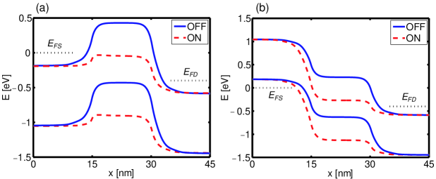
For the channel and source/dain extension, we use an armchair-edge Graphene Nanoribbon (aGNR) with (width1.6 nm) that leads to an intrinsic bandgap of = 0.86 eV with H-terminated edges where edge bond relaxation is considered with a modified tight-binding parameter (, eV) [11]. The nominal device has double-gate geometry with 1.6 nm thick gate oxide ( = 16) resulting in an equivalent oxide thickness EOT = 0.4 nm. The channel length is = 15 nm, and the source/drain extension is = 15 nm. Source/drain doping density, is set to , which is equivalent to . A power supply voltage of V is assumed. The electronic transport is modeled by solving the open boundary Schrödinger equation using non-equilibrium Green’s function (NEGF) formalism within the nearest neighbor tight-binding approximation in a orbital basis set (see for example [8] and references therein) that automatically accounts for electron and hole currents. The NEGF transport equation is solved self-consistently with a three-dimensional solution of Poisson equation. For comparison, we explored two different types of structures. Figure 1(a) shows energy band diagram of an n-i-n MOSFET device that we shall use as a reference. When the GNR is p-doped at the source, the resulting p-i-n structure will constitute a tunneling FET [Fig. 1(b)].
III Results
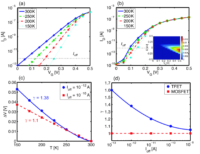
characteristic for a GNR MOSFET is shown in Fig. 2(a) for various temperatures. In general, the subthreshold swing of a MOSFET can be written as , where , often called the body factor, is a constant and equal to the ratio of the supply voltage to the channel potential. Two things can be easily inferred from this expression: First, the thermionic emission current is expected to give a constant subthreshold swing for a given temperature and second, the subthreshold swing is expected to change linearly with temperature. This is exactly what we see in Fig. 2(a).
By contrast, the characteristics of a TFET ([Fig. 2(b)]) show significant non-linearity in the subthreshold region both over the voltage range and also over the temperature. In absence of an analytical expression as in the case of MOSFETs, it is difficult to understand the underlying physics in a simple manner. In order to analyze the non-linear temperature dependence in TFETs, we have plotted the shift of voltage, with temperature at various current levels denoted as in Fig. 2(c). The is measured from and it is fitted with the following equation:
| (1) |
The rationale for using Eq. (1) is that the parameter gives information about non-linearity with temperature. At the same time, any dependence of with respect to gives information about the non-linearity in the subthreshold region as a function of gate voltage. Thus both non-linearities in the tunneling current can be captured in a single parameter . In Fig. 2(d), we show as a function of . We see that, for MOSFET (the squares), is independent of and it is equal to 1. This means that the subthreshold swing for a MOSFET is linear with temperature and independent of gate voltage. On the other hand, for the TFET (the circles), is larger than 1 and it also varies as a function of . The non-linearity in in Fig. 2(d) thus carries a telltale signature of the tunneling phenomena itself, and experimental measurements can be characterized in this way to distinguish between thermionic emission type and band-to-band tunneling currents. Fig. 2(d) is the central result of our paper.
To understand the non-linearity in , we note that, in the ballistic case, the current can be written as
| (2) |
where is transmission, is the plank’s constant and and are the Fermi functions of the source and the drain terminals, respectively. The inset in Fig. 2(b) shows the transmission at K as a function of energy, and gate voltage, . Taking this numerical result, we re-calculated current from Eq. (2) at all other temperatures so that the transmission is kept fixed for all temperatures and the variation in temperature only enters in the Fermi functions. The calculated currents are plotted as individual markers in Fig. 2(a) and (b). We see that this pseudo-analytical treatment shows a reasonably good agreement with the full numerical results for both the MOSFET and the TFET structures. This clearly indicates that any non-linearity that we see in the tunneling current as a function of temperature is coming from . Using this fact, we can now construct a simple picture of the underlying physics. The band-diagram shown in Fig. 1(a) shows that in case of the MOSFET structure, the current has the full contribution of the Fermi tail. By contrast, as Fig. 1(b) shows, the Fermi tail is cut off by the bandgap for the TFET. This phenomenon of Fermi-tail cut-off is well known and is credited for the lowering of subthreshold swing in a tunnel transistor. What we show here is that this cut-off is also responsible for the non-linearity in the subthreshold swing with temperature and can be characterized as shown in Fig. 2(d).
Another very important conjecture from Eq. (2) is its generality. No matter what material is used, the temperature dependence is qualitatively going to be the same since the specifics of the difference in materials will only modify the transmission function . Strictly speaking, transmission should also be affected by temperature through the charge self-consistency. However, as long as the Fermi level is not right at the band edge and the temperature is not extremely low, the temperature dependence of is negligible.
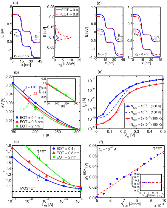
Next we examine how this non-linearity is further influenced by various device parameters. First we look at the equivalent gate oxide thickness (EOT) that changes the vertical field. In our simulation this field is varied by changing the dielectric constant of the insulator. What we see from Fig. 3(b) and (c) is that the non-linearity in increases significantly with increasing EOT. To explain this behavior we plotted the band profile of the TFET for EOT = 0.4 (solid line) and 0.8 nm (dashed line) on the left panel of Fig. 3(a). It is seen that larger EOT makes the tunneling barrier thinner since the gate loses its control over the contacts right outside the channel region. A thinner barrier effectively acts to cut less of the tail compared to a thicker barrier as confirmed by the fact that the current spectrum of a larger EOT exists at higher energy [dashed line on the right panel in Fig. 3(a)]. It is important to note that a larger EOT results in a thinner barrier and thus moves the effective band-edge away from the Fermi level, thereby increasing the overall non-linearlity. In turn, this increased non-linearity can carry the information of EOT itself. Note that in comparison, the and for the MOSFET are unaffected by the change of EOT [see the inset of Fig. 3(b) and dashed line in 3(c)].
Figure 3(d-f) show the effects of source/drain doping density on the temperature dependence. Two observations can be made from the band profiles [Fig. 3(d)]: Lower doping causes (i) a decrease in the energy window for carrier injection, and (ii) an increase in the thickness of the tunneling barrier. We see from Fig. 3(e) that the voltage shift is drastically reduced with the low doping density, which can again be understood from the Fermi tail cut-off. A higher density moves the Fermi level away from the band-edge, effectively lowering the amount of Fermi-tail truncation by the band gap. As discussed earlier, this increases the non-linearity in the current. On the other hand, a lower density moves the Fermi level closer to the band-edge effectively reducing the non-linearity. In order to quantify the effect of doping on in TFETs, is plotted as a function of in Fig. 3(f). For the simulated range, we see a nearly linear dependence of with doping density. By contrast, is almost independent of source/drain doping for the MOSFET structure [see the inset in Fig. 3(f)]. Again here, in addition to the fact that it is distinctly different from the MOSFET current, the tunneling current in the TFET may provide information about the source/drain doping density itself.
In this work, we have ignored phonon scattering that may bring in its own temperature dependence in the tunneling current and will have to be studied carefully. Nonetheless, this should merely determine the exact degree of non-linearity in , keeping the qualitative picture depicted in Fig. 2(d) intact. Note that, even in presence of the aforementioned non-idealites, the MOSFET retains a linear temperature dependence in subthreshold swing, indicating a flat , and this fact has been verified by many experiments, e.g., [12]. Notably first principles study suggests that change of bandgap with temperature for graphene nanoribbons is minimal [11].
IV Conclusion
To summarize, based on an atomistic quantum transport simulation, we predict that the band-to-band tunneling current in a GNR TFET should exhibit unique non-linearity with temperature that carries a distinct signature as a function of various device quantities such as doping and vertical electric field, where MOSFET characteristics remain unaffected. By constructing a pseudo-analytical model to compare with our numerical results, we have shown that these unique characteristics should be independent of the channel material and generally applicable to any TFET. Thus we believe that the temperature dependence can be used as a generic spectroscopic tool that may give important insights into band-to-band tunneling phenomena.
References
- [1] A. Bowonder et al., “Low-voltage green transistor using ultra shallow junction and hetero-tunneling”, Int. Work. on Junc. Tech. (IWJT), pp. 93-96, 2008.
- [2] T. Krishnamohan et al., “Double-Gate Strained-Ge Heterostructure TFET with Record High Drive Current and less than 60 mV/dec Subthreshold Slope”, IEDM Tech. Dig., 2008.
- [3] J. Appenzeller et al., “Band-to-Band Tunneling in Carbon Nanotube Field-Effect Transistors”, Phys. Rev. Lett., vol. 93, no. 19, p. 196805, 2004.
- [4] M. Luisier et al., “Atomistic Full-Band Design Study of InAs Band-to-Band Tunneling Field-Effect Transistors”, IEEE Elec. Dev. Lett., vol. 30, no. 6, p. 602, 2009.
- [5] A. S. Verhulst et al., “Boosting the on-current of a n-channel nanowire tunnel field-effect transistor by source material optimization”, J. Appl. Phys., vol. 104, p. 064514, 2008.
- [6] S. O. Koswatta et al., “Performance Comparison Between p-i-n Tunneling Transistors and Conventional MOSFETs”, IEEE Trans. Elec. Dev., vol. 56, no. 3, pp. 456-465, 2009.
- [7] Q. Zhang et al., “Graphene Nanoribbon Tunnel Transistors”, IEEE Elec. Dev. Lett., vol. 29, no. 12, pp. 1344-1346, 2008.
- [8] P. Zhao et al., “Computational Study of Tunneling Transistor Based on Graphene Nanoribbon”, Nano Lett., vol. 9, no. 2, pp. 684-688, 2009.
- [9] E.O. Kane, “Theory of Tunneling”, J. Appl. Phys., vol. 32, no. 1, p. 83, 1961.
- [10] A. Motayeda et al., “GaN-nanowire/amorphous-Si core-shell heterojunction diodes”, Appl. Phys. Lett., vol. 93, p. 193102, 2008.
- [11] Y. W. Son et al., “Energy gaps in graphene nanoribbons”, Phys. Rev. Lett., vol. 97, no. 21, p. 216803, 2006.
- [12] L. Michalas et al., “An experimental study of the thermally activated processes in polycrystalline silicon thin film transistors”, Microelectronics Reliability, vol. 47, no. 12, pp. 2058-2064, 2007.