Instability of two dimensional graphene: Breaking sp2 bonds with soft X-rays
Abstract
We study the stability of various kinds of graphene samples under soft X-ray irradiation. Our results show that in single layer exfoliated graphene (a closer analogue to two dimensional material), the in-plane carbon-carbon bonds are unstable under X-ray irradiation, resulting in nanocrystalline structures. As the interaction along the third dimension increases by increasing the number of graphene layers or through the interaction with the substrate (epitaxial graphene), the effect of X-ray irradiation decreases and eventually becomes negligible for graphite and epitaxial graphene. Our results demonstrate the importance of the interaction along the third dimension in stabilizing the long range in-plane carbon-carbon bonding, and suggest the possibility of using X-ray to pattern graphene nanostructures in exfoliated graphene.
The existence and stability of two dimensional materials has been a fundamental yet long-debated subject. Graphene, a purely one atom thick two dimensional material formed by carbon atoms arranged in a honeycomb lattice, was previously presumed not to exist because strictly two dimensional materials are thermodynamically unstable WMTheorem ; Mermin ; Landau . The recent discovery of graphene NovoselovSci ; PNAS has raised renewed interest regarding the long debated issue about the stability of two dimensional materials. Although it has been proposed recently that the ripples - corrugation along the third dimension in free-standing exfoliated graphene samples help to stabilize graphene GrapheneRipple ; Fasolino ; Carlsson , no direct experimental evidence about what causes the stability of the sp2 bonds has been obtained so far. Here we present direct experimental proof that it is indeed the interaction along the third dimension that drives the stability of the graphene sheet. In particular we show that the closer the graphene sample is to a two dimenstional crystal, the easier it is for the sp2 bonds to be broken under soft X-ray irradiation, resulting in nanocrystalline structures. This conclusion was based on a sysmatic study of various kinds of graphene samples with different amount of interaction along the third dimensionality, including exfoliated graphene on SiO2, suspended exfoliated graphene, and epitaxial graphene on SiC, and by combining two important techniques - X-ray absorption spectroscopy which is sensitive to the sp2 bonding, and Raman spectroscopy which is sensitive to the edges of the graphene samples Pimenta07 ; Ferrari2 . Our results show direct evidence about the instability of two dimensional graphene, and points out a possible route of using X-rays to engineer graphene nanoribbons.
The samples studied were exfoliated graphene samples on SiO2/Si and epitaxial graphene on SiC. The thickness of exfoliated graphene samples is characterized by optical contrast ShenNanoLett2007 ; GeimSci2008 and confirmed by Raman measurements Ferrari ; Graf . The thickness of epitaxial graphene is characterized by low energy electron microscope (LEEM) Hibino . Although the overall electronic structure of graphene is preserved in both types of graphene samples, the interaction along the third dimension is much stronger in epitaxial graphene than exfoliated graphene. This is manifested by the formation of a first carbon rich layer strongly bonded with the SiC substrate Seyller , and the opening of a gap in the bands for the first graphene layer NatMat ; KimAbInitio . X-ray absorption spectroscopy (XAS) spectra at the C 1s edge were taken with photoemission electron microscope (PEEM) at PEEM2 of the Advanced Light Source (ALS) in Berkeley. The microscope is operated in the total electron yield (TEY) mode by recording the intensity maps while sweeping the photon energy across the C K edge. The photon flux was cut down to only 1/3 of the regular value to decrease the X-ray radiation damage on the sample. Raman spectra were taken on a commercial system (Renishaw inVia) at a wavelength of 514 nm (Argon laser). Special care was taken to minimize laser exposure on samples and subsequent spectra at the same spot showed no change. The spatial resolution of both techniques allows easy detection of each graphene region with different thickness.
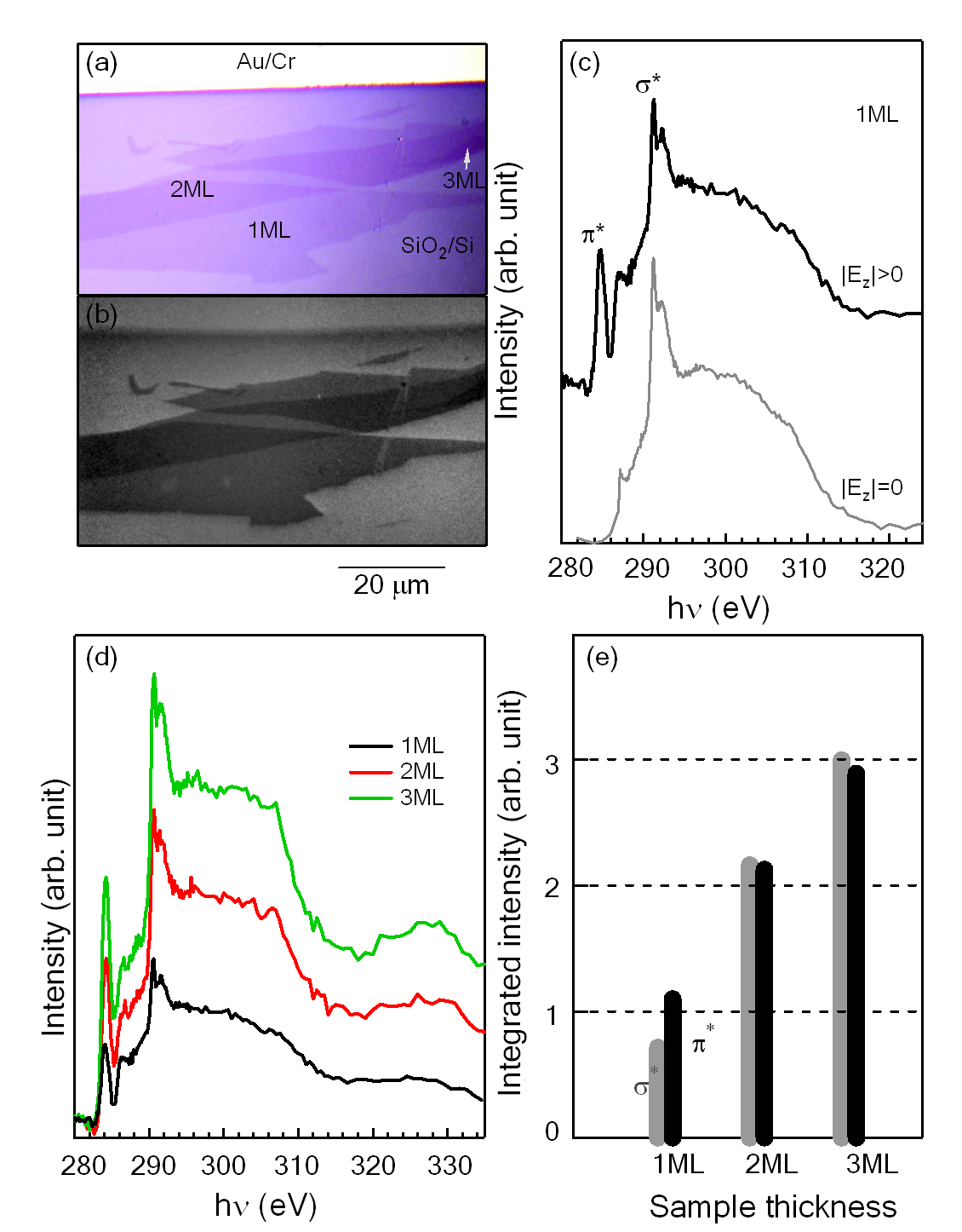
Figure 1 (a) shows the optical image of a typical exfoliated sample. Clear optical constrast can be observed between regions of graphene with different sample thickness PNAS . Figure 1(b) shows the PEEM image taken at 279 eV photon energy before the C 1s K edge on the same sample. Similar to the optical image (Figure 1a), strong intensity contrasts between different regions are observed in the PEEM image shown in Figure 1(b). Thicker graphene regions will appear darker in the pre-edge spectra because photoelectrons travel through more materials before being emitted to the vacuum, thus making PEEM another powerful tool to capture the thickness of graphene films. Figure 1(c) shows the C 1s XAS spectra taken on single layer exfoliated graphene with two different polarizations. The two main features at 285 eV, and at 292 eV, correspond respectively to the orbitals at the K and M points of the Brillouin zone and to the orbitals at the point PolarizationDep . Their in-plane and out-of-plane characters are confirmed by the dependence from the polarization of the incident photons (Figure 1(c)) PolarizationDep . More specifically, when the light polarization is in-plane, only the in-plane orbital at 292 eV contributes to the C 1s edge, while when the out-of-plane polarization component increases, the intensity of the feature at 285 eV strongly increases.
In Figure 1(d) we show the C 1s spectra of exfoliated graphene for different sample thickness. As in Figure 1(c), the feature and the splitting of the orbitals are observed in all the spectra, independent of the sample thickness. The main difference is that as the thickness increases, the intensity of the and features increases.
The high energy resolution and sample quality of this experiment has enabled us to clearly resolve the splitting of the peaks, not observed in a previous study GrioniPEEM , and hence to quantify the thickness dependence of the absorption spectra and directly compare it to the optical reflectivity data. In Figure 1(e) we show the integrated absorption intensity, determined from the area underneath the and orbitals near the C K edge. The data clearly show that the intensity of the and the orbitals scales linearly with the sample thickness for up to three layers. Interestingly, this is in close analogy to the quantized steps observed in optical reflectivity and transmission for different graphene thickness ShenNanoLett2007 ; GeimSci2008 , which are defined only by the fine structure universal constant GeimSci2008 . This result suggests that, even at higher photon energies the universality still holds and the absorption spectra is still related to the universal constant , the parameter that defines the optical transparency of graphene.
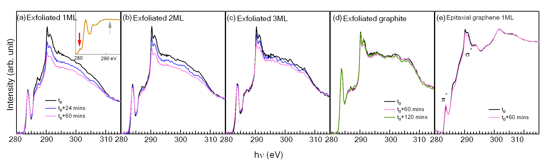
Figure 2 shows the time evolution of the absorption spectra for exfoliated (panels a-d) and epitaxial (panel e) graphene. The relative intensity ratio of the to the orbital show a clear time dependence from X-ray exposure. More specifically, the time dependence of the spectra is strongest for exfoliated single layer graphene (Figure 2(a)), as measured from the 24 change in the intensity ratio of the orbital to the orbital, and decreases significantly as the number of layer increases, from 20 in bilayer to 15 in trilayer graphene. These findings suggest a strong radiation-induced damage of the exfoliated graphene upon soft X-ray exposure, a surprising result considering the inert character of carbon. This is reminiscent of the radiation-induced damage observed in carbon rich biological samples Molodtsov . We note that, although the radiation-induced damage presented here is observed for all the samples studied (more than five samples in total), in some cases the absorption spectra of single layer graphene shows more dramatic changes. In an extreme case (inset in Figure 2(a)), the signal of the orbital completely disappeared (pointed to by a gray arrow) and an additional peak arose before the adsorption edge (pointed to by a red arrow), reminiscent of the edge states observed in nanographite sample EdgeStates .
The strong radiation-induced change of the single layer exfoliated graphene (Figure 2(a)) is in contrast to the almost negligible effect observed on the epitaxial sample (Figure 2(e)). As for the exfoliated sample, the two main features in the spectra are the and the orbitals, which occur at the same energy, a further confirmation that the overall electronic structure of exfoliated and epitaxial graphene is similar in nature. In this case however, the relative intensity of the to the peak is much weaker, suggesting that the derived states are partially occupied. This is likely due to a charge transfer from the buffer layer, in agreement with photoemission measurements reporting an highly doped nature of this sample NatMat . Note that, in addition to these main features, other peaks are observed above the peak, likely due to the substrate, as observed from a direct comparison with the absorption spectra of SiC SiCXAS .
The time dependence of the spectra in Figure 2(e) clearly shows that the epitaxial sample is very stable and the damage induced by x-ray irradiation is negligible, despite the much longer exposure time. This result is in striking contrast with the strong time dependence observed in the exfoliated sample (Figure 2a). Note that these two types of samples were measured in the same chamber under the same conditions, and therefore this substantial difference in stability should be attributed to their intrinsic nature, e.g. the different strength of interaction along the third dimension, and not an artifact of the measurements.

To better understand the origin of this radiation-induced change, we compare Raman measurements on the same samples measured before and after exposure to soft X-rays (see Figure 3). Before exposure, the exfoliated graphene sample shows a sharp G peak induced by the zone center E2g phonon at 1570 cm-1, and a strong 2D peak (overtone of the zone boundary A1g phonon) at 2700 cm-1. The 2D peak in single layer graphene shows a single component, while the 2D peak for bilayer, trilayer graphene and many layer graphite is broader and contains multiple components, in agreement with previous studies Ferrari ; Graf . The sharpness of the G and 2D peaks, as well as the absence of the disorder-induced D peak at 1360 cm-1 Pimenta07 ; Ferrari2 ; Vidano , D′′ peak at 2950 cm-1, shows that the samples under study are of very high quality, and the amount of disorder is negligible. However, after X-ray exposure, the Raman spectra show significant changes in all the exfoliated samples, although the degree of change decreases from single layer to trilayer graphene and almost disappear for graphite, in line with the absorption results previously discussed. More specifically, we observe the appearence of a huge D peak at 1360 cm-1, as well as the appearance of D′ peak at 1620 cm-1 and D′′ peak at 2950 cm-1. These changes are accompanied by the broadening of both the G (1570 cm-1) and 2D (2700 cm-1) peaks. In line with the absorption results (see Figure 2), the comparison between graphene samples with different thickness suggests that the largest radiation-induced changes occur on the single layer exfoliated graphene sample. On the contrary, the Raman spectrum for the single layer epitaxial graphene shows negligible change, although it has been exposed to X-ray for a much longer time ( 10 hours), once again pointing to the different nature between exfoliated and epitaxial graphene, and a better stability of the latter to X-ray irradiation.
The results presented here point to a scenario where the X-rays locally break the sp2 bonding giving rise to small crystallites within the same graphene sheet. This is supported by: 1) the decrease, or in some cases even the disappearence, of the -orbital-related signal in the absorption spectra (Figure 2), suggesting a decrease of sp2 bonded carbon atoms; 2) the appearence of a broad pre-edge feature (inset of figure 2(a)) in the absorption spectra, similar to that observed in nanographite edges EdgeStates ; 3) the appearence of strong D, D′ peaks in the Raman spectra (Figure 3), associated with an increase of broken carbon bonds and edges states Pimenta07 ; Ferrari2 ; Vidano ; Graf ; FerrariRamanDisorder ; 4) the broadening of the G and 2D peak in the Raman spectra, suggestive of phonon confinement. The average crystallite size estimated from the ratio between the G and D peaks in the Raman spectra Pimenta07 changes from 7 nm in single layer exfoliated graphene to 10 and 12 nm in bilayer and trilayer exfoliated graphene respetively, pointing to a smaller irradiation induced bond-breaking effect in thicker exfoliated graphene samples.
There are a few possibilities about the bond-breaking mechanism, and further investigation is needed to pin down the exact mechanism. First, the higher probability of bond breaking by X-rays in insulating samples BondbreakingMechanism suggests that the bond-breaking in graphene, which is a semimetal, might be caused by the ejection of electrons into the vacuum and the insufficient restoration of the ejected electrons as a result of its low charge carrer concentration. This is particularly so considering that the SiO2 layer underneath the graphene sample is quite insulating as well. Another possibility is that in exfoliated graphene, the SiO2 substrate or even residual water between graphene and the SiO2 layer might act as a “catalyst” for the sp2 bond-breaking through formation of epoxy groups or carbon mono-oxide groups. To test the second possiblity, we have measured two bilayer graphene samples partially suspended on a few m width trenches and we have detected a very similar amount of D peak in both the suspended and unsuspended regions after X-ray irradiation. This suggests that whatever the bond breaking mechanism is, it must be intrinsic to the exfoliated graphene, and irrelavant of the SiO2 substrates or the trapped water or gas between graphene and the SiO2. As shown above, the radiation-induced bond-breaking effect also decreases when the interaction along the third dimension increases either by increasing the number of layers or through a stronger interaction with the substrate, suggesting the important role of the interaction along the third dimensionality.
In summary, we found that single layer exfoliated graphene is unstable under soft X-ray exposure, resulting in local breaking of the sp2 bonding and the formation of small crystallites within the sample. As the interaction along the third dimension increases, either by increasing the sample thickness or through stronger bonding with the substrate, as in the case of epitaxial graphene, the graphene sample becomes more stable. These results point to the crucial role of the interaction along the third dimension in stabilizing quasi-two dimensional graphene. Finally, this ability to easily break the carbon-carbon bonds suggests the possiblity of using X-rays or even lasers LaserRadiation to “write” graphene nanostructures, an alternative to standard writing techniques. Further studies are needed to investigate where the bonds break CogSci and to achieve a fine control of the amount of broken bonds.
Acknowledgements.
We thank D.-H. Lee, A.K. Geim and A.C. Ferrari for useful discussions. The photoemission and Raman measurements were supported by the Division of Materials Sciences and Engineering, Office of Basic Energy Sciences of the U.S. Department of Energy under Contract No. DE-AC03-76SF00098. AZ and COG acknowledge the DOE grant DE-AC02-05CH11231 for sample preparation and Raman characterization.References
- (1) Mermin, N.D., Wagner, H. Phys. Rev. Lett. 17, 1133 (1966).
- (2) Mermin, N.D. Phys. Rev. 176, 250-254 (1968).
- (3) Landau, L.D., Lifshiftz, E.M. Statistical Physics, Part I (pergamon, Oxford, 1980).
- (4) K.S. Novoselov et al, Science 306, 666 (2004).
- (5) K.S. Novoselov et al, Proc. Natl. Acad. Sci. U.S.A. 102, 10451 (2005).
- (6) J.C. Meyer et al, Nature 446, 60 (2007).
- (7) A. Fasolino, J.H. Jos, M.I. Katsnelson, Nature Mat. 6, 858 (2007).
- (8) Carlsson, J.M. Buckle or break. Nature Mat. 6, 801 (2007).
- (9) Ferrari, A.C. Solid State Commun. 143, 47 (2007).
- (10) M.A. Pimenta et al, Phys. Chem. Chem. Phys. 9, 1276-1291 (2007).
- (11) Z.H. Ni et al, Nano Letters 7, 2758 (2007).
- (12) R.R. Nair et al, Science 320, 1308 (2008).
- (13) A.C. Ferrari et al, Phys. Rev. Lett. 97, 187401 (2006).
- (14) D. Graf et al, Nano Lett. 7, 238-242 (2007).
- (15) H. Hibino et al, Phys. Rev. B 77, 075413 (2008).
- (16) K.V. Emtsev et al, Mater. Sci. Forum 556-557, 525 (2007).
- (17) S.Y. Zhou et al, Nature. Mat. 6, 770 (2007).
- (18) S. Kim, J. Ihm, H.J. Choi, Y.W. Son, Phys. Rev. Lett. 100, 176802 (2008).
- (19) R.A. Rosenberg, P.J. Love, V. Rehn, Phys. Rev. B 33, 4034 (1986).
- (20) D. Pacile et al, Phys. Rev. Lett. 101, 066806 (2008).
- (21) A. Kade et al, J. Phys. Chem. B 111, 13491-13498 (2007).
- (22) S. Entani et al, Appl. Phys. Lett. 88, 153126 (2006).
- (23) M. Pedio et al, Physica Scripta T115, 308 (2005).
- (24) R.P. Vidano, D.B. FIschbach, Solid State Commu. 39, 341-344 (1981).
- (25) A.C. Ferrari, J. Robertson, Phys. Rev. B 61, 14095 (2000).
- (26) J. Cazaux, J. Microscopy 188, 106-124 (1997).
- (27) A. Hu, M. Rybachuk, Q.-B. Lu, W.W. Duley, Appl. Phys. Lett. 91, 131906 (2007).
- (28) Girit, Ç.Ö. et al, Science 323, 1705-1708 (2009).