Half-Metallic Silicon Nanowires: Multiple Surface Dangling Bonds and Nonmagnetic Doping
Abstract
By means of first-principles density functional theory calculations, we find that hydrogen-passivated ultrathin silicon nanowires (SiNWs) along [100] direction with symmetrical multiple surface dangling bonds (SDBs) and boron doping can have a half-metallic ground state with 100% spin polarization, where the half-metallicity is shown quite robust against external electric fields. Under the circumstances with various SDBs, the H-passivated SiNWs can also be ferromagnetic or antiferromagnetic semiconductors. The present study not only offers a possible route to engineer half-metallic SiNWs without containing magnetic atoms but also sheds light on manipulating spin-dependent properties of nanowires through surface passivation.
pacs:
71.70.Ej, 73.21.Hb, 73.22.DjIt is widely believed that nanowires can be the most promising candidates for the basic building blocks of future nanoelectronics, as they could be essentially useful in engineering diverse nanodevices such as field-effect transistors, logic gates, DNA sensors, etc. nanowire ; device1 ; device2 ; device3 Thus, the nanowires with thin diameters small1 ; small2 were actively studied both experimentally and theoretically in the past years. Recently, particular attention was paid on the ultrathin silicon nanowires (SiNWs) Chou ; basic ; doping ; B+DB ; 001a ; 001b , as they not only have unusual electronic properties of scientific interest, but also could be potentially incorporated into nowadays well-developed Si-based electronic technology.
The properties of ultrathin nanowires can be modified by adjusting diameters and orientations, conducting the surface passivation, or introducing dopants, etc. For SiNWs, among other things, it is known that (i) due to surface reconstruction, SiNWs along [100] direction with diameters smaller than 1.7 nm prefer a square cross section with sharp corners where the electrons are quite localized 001a ; 001b ; shape ; sharpcorner ; (ii) the ultrathin SiNW that is saturated with H atoms on surface can show a semiconducting behavior basic , and if it is substitutionally doped with nonmagnetic elements like B or P, the main bands of impurities distribute at the top of valence bands B+DB ; (iii) H-passivated ultrathin SiNWs along [100] direction interstitially doped by a certain density of transition metals such as Co or Cr can have a half-metallic ground state HM1 ; (iv) when the H-passivated nanowires or surfaces have an isolated or a single row of surface dangling bonds (SDBs), there is a band contributed by the SDBs crossing the Fermi level (FL) B+DB ; P+DB ; BP+DB ; SiGe+DB ; C+DB , and if the spin polarization is considered, the band splits into two discrete bands, respectively, below and above the FL C+DB , leading to two band groups formed in the case of multiple SDBs Si+DB .
In the present Letter, by means of calculations we have found that, for an ultrathin H-passivated SiNW along [100] direction with multiple SDBs at symmetrical positions and substitutionally doping B atoms at the center of cross section, a ferromagnetic (FM) configuration is favored as the ground state, and such a SiNW is a half-metal with 100% spin polarization, namely, it is insulating for one spin direction while metallic for the opposite spin direction at the FL. To the best of our knowledge, this is the first time to report a novel type of half-metallic SiNWs with multiple SDBs and nonmagnetic doping, in contrast to the previous study where the half-metallic SiNWs were obtained by doping transition metals HM1 . This poses a possible route to make half-metallic SiNWs through manipulating the surface passivation and introducing nonmagnetic dopants.
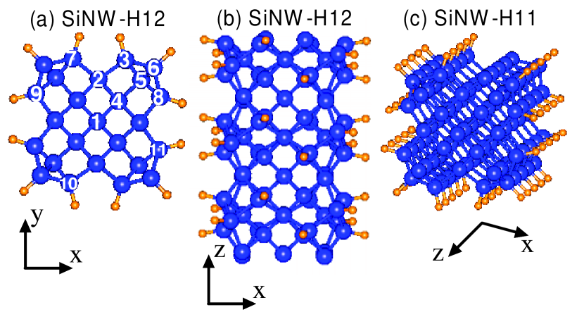
Our calculations were based on the density functional theory DFT with generalized gradient approximation expressed by PBE functional PBE , employing norm-conserving pseudopotentials T-M and linear combinations of atomic orbitals. The SIESTA code SIESTA ; ESPRESSO with double-zeta polarized basis sets was used to perform spin-polarized calculations. The energy cutoff was 180 Ry, and the total energy convergence criterion was 10-5 eV. All structures were fully relaxed by the maximum force tolerance of 0.015 eV/, and the lattice constant along the wire axis was optimized for each structure. Among the SiNWs of 25 Si atoms per unit [Fig. 1(a)] with different SDBs, the separation between two adjacent wires was kept as 15.27 (0.02) . The Brillouin zone along the axial direction was sampled with 15 k-points.
Figs. 1(a) and (b) depict the ultrathin SiNW along [100] direction passivated with H atoms without SDBs (labeled by SiNW-H12), where there are 25 Si and 12 H atoms per unit cell. In SiNW-H12, the diameter is about 11 including H, and about 8 excluding H. The positions in axis of the adjacent Si atoms at positions 3 and 4 [Fig. 1(a)] differ only by 0.009 . Note that the H saturated SiNW-H12 is semiconducting basic . For the SiNW with single SDB per unit [denoted by SiNW-H11, Fig. 1(c)], there is one unpaired electron at the SDB in each unit, and the total magnetic moment is 1.00 per unit cell ( is Bohr magneton). In SiNW-H11, the Si atom with SDB [position 3 in Fig. 1(a)] is stretched 0.047 outer than the Si at position 4 that is still passivated with H, and the energy for generating a single SDB per unit is 3.52 eV. We compared different spin configurations by employing a supercell with two unit cells (including two adjacent SDBs), and disclosed that the FM configuration is favored as the ground state, with the energy of 11.3 meV per unit cell lower than the antiferromagnetic (AF) configuration, and 155.6 meV per unit lower than the nonmagnetic (NM) configuration. It turns out that the SiNW-H11 is a FM semiconductor with an indirect gap of 0.59 eV.
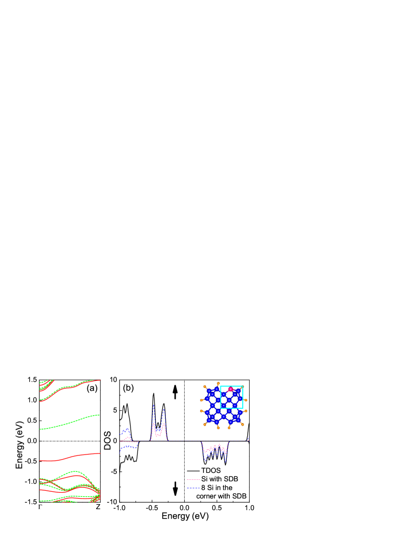
The electronic structure and density of states (DOS) of FM SiNW-H11 are presented in Fig. 2. It can be seen that there are two split bands just above and below the FL [Fig. 2(a)]. The upper band is of minority spins (), while the lower is of majority spins (), which correspond to the half-filled band crossing the FL if the spin polarization is ignored, similar to the case at C(001) surface C+DB . For the bands away from the FL, there is merely a small displacement between the spin-up and spin-down subbands, which is close to the SiNW-H12. The constituents of the two split bands are clearly manifested in the projected DOS (PDOS): The Si atom with a SDB contributes 44.9% to the total DOS (TDOS), which dominates overwhelmingly among all atoms, and the 8 Si atoms in the corner including the SDB contribute 82.9% to the TDOS, as shown in Fig. 2(b). This indicates that the two split bands are formed primarily by the unpaired electron of SDB and the electrons closely around the SDB.
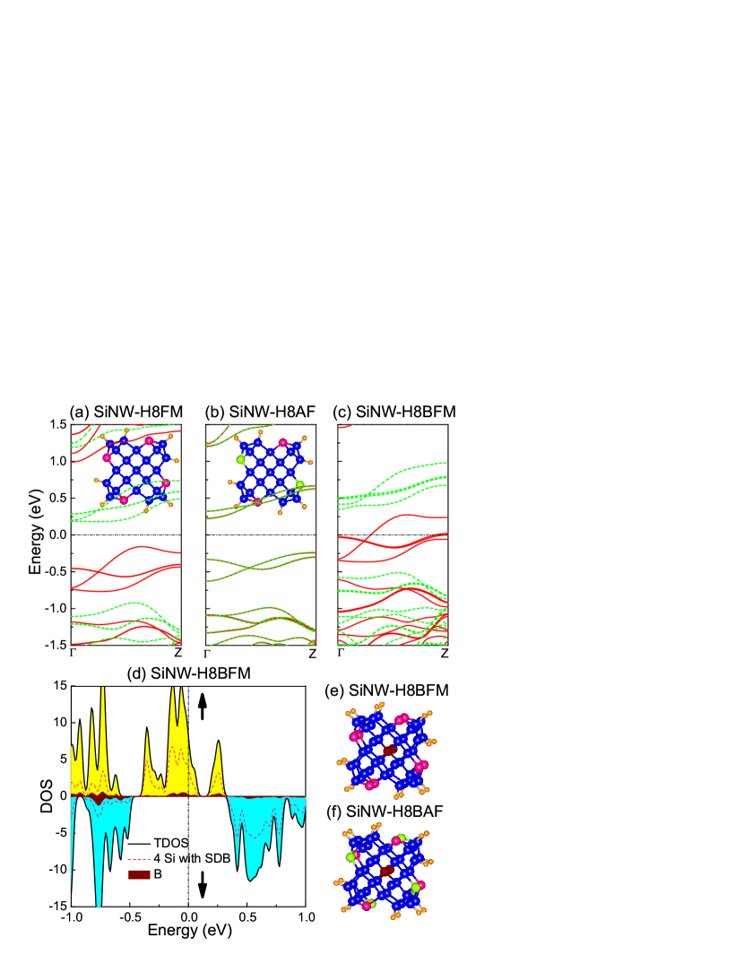
Now let us look at the SiNW with multiple SDBs. Without loss of generality, the case of four SDBs per unit cell located symmetrically on each edge of the cross section will be calculated, as shown in Figs. 3(a) and (b), labeled by SiNW-H8. In comparison to the SiNW-H11, the FM configuration of SiNW-H8 [SiNW-H8FM, Fig. 3(a)] has more split bands, which are separated into two groups above and below the FL, and each group includes four bands of the same spin species (either spin up or down), where there is one band degenerate with another in each group. The magnetic moment is 4.00 per unit cell. However, the SiNW-H8FM is merely a metastable state. The ground state has an AF configuration [SiNW-H8AF, Fig. 3(b)], where the SDBs on adjacent edges have opposite spin alignments, with an energy lower than SiNW-H8FM by 26.9 meV per unit cell. The average energy for generating each SDB in this case is 3.55 eV. The spin-up and spin-down bands of the SiNW-H8AF coincide, and is zero, as revealed in Fig. 3(b). Therefore, SiNW-H8 is an AF semiconductor with an indirect gap of 0.47 eV. In the band structure of SiNW-H8FM [Fig. 3(a)], the indirect gap between the bands of majority and minority spins is 0.34 eV, which is so small that it could be possible to generate a perfect half-metallic behavior in the SiNW-H8 so long as the two conditions are satisfied: (i) The FL is slightly shifted upward or downward to intersect the split bands of the same spin species; (ii) The FM configuration of SDBs should be the ground state. To meet with the conditions, it may be convenient to conduct nonmetallic dopings (such as B or P).
By substitutionally doping one B atom at the center of the cross section [position 1 in Fig. 1(a)] of the SiNW-H8FM (labeled by SiNW-H8BFM), we found that the SiNW-H8BFM is the ground state, and the FL moves indeed downward intersecting the majority spin bands, giving rise to a half-metallic behavior, as shown in Fig. 3(c). This is also manifested in Fig. 3(d), where the DOS of majority spin at the FL () is 8.28/eV, while the DOS of minority spin is zero, leading to the spin polarization . The indirect band gap of minority spin is 0.86 eV. The total magnetic moment of SiNW-H8BFM is per unit cell, while the local moment of each Si atom with SDB is 0.51 (0.01) , that is 0.11 lower than SiNW-H8AF. As there are three spin-up bands at different points in the Brillouin zone crossing the FL, it is hard to open a gap due to Peierls instability 001b . Thus, the half-metallicity in the SiNW-H8BFM is robust. We also examined possible magnetic configurations [FM, AF and ferrimagnetic (FI)] in a supercell with either one or two unit cells, respectively, together with NM (SiNW-H8BNM, spin-unpolarized) calculations, and observed that apart from the FM ground state [SiNW-H8BFM, Fig. 3(e)], the lowest metastable state is an AF metal [SiNW-H8BAF, Fig. 3(f)]. The total energies of SiNW-H8BNM and SiNW-H8BAF are 309.2 meV and 21.5 meV per unit cell, respectively, higher than that of SiNW-H8BFM. Based on the energy difference between the SiNW-H8BFM and SiNW-H8BAF, we can estimate that at the temperature lower than 250K, the half-metallic property in the SiNW-H8B can be retained.
Doping P at the center in a FM configuration of SiNW-H8 (labeled by SiNW-H8PFM) is similar to the SiNW-H8BFM except that the FL moves upward crossing the spin-down bands, resulting in the half-metallicity for minority spins. However, the ground state for this case is a FI metal, where the total magnetic moment per unit cell, and the total energy is slightly lower than SiNW-H8PFM by 3.2 meV per unit cell. Compared with the AF ground state of SiNW-H8, doping B at the center will decrease both the charge of each SDB and the diameter of the SiNW, leading to a FM ground state, while doping P brings about inverse changes, making a FI ground state. Besides, it is unraveled that in spite of doping B, P or not, if there are two SDBs in one corner [at positions 3 and 8 in Fig. 1(a)] or in one edge (at positions 3 and 7), the FM configuration appears not to be the ground state.
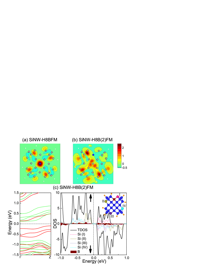
For the SiNW-H8BFM, Fig. 4(a) indicates that the spin density () distributes identically in each of the four corners with SDB, where () is the number density of electrons with spin up (down). The dopant B at the center has a homogeneous effect on the symmetrical SDBs, leading to the half-metallicity. If doping B takes place at the edge [position 2 in Fig. 1(a)] instead of the center with the FM configuration [SiNW-H8B(2)FM, Figs. 4(b) and (c)], there are three spin-up bands just below the FL, and four spin-down bands and one spin-up band just above the FL. The four Si atoms with SDBs contribute to the PDOS distinctly, among which the one [red Si (I) in Fig. 4(c)] adjacent to the B atom plays an overwhelming role. It is also confirmed by the spin density distribution in Fig. 4(b), where the spin density of the 1/4 cross section around Si (I) is nearly zero, totally different from those in other three corners. The local moment of Si (I), (II), (III) and (IV) is 0.09, 0.58, 0.63 and 0.61 , respectively. In general, doping B at any position other than the center will give a semiconductor. The total energy per unit cell of doping B atoms at position 4, 2, 3, 5, 6 and 7 [Fig. 1(a)] is 0.36, 0.52, 0.70, 0.46, 0.58 and 0.73 eV, respectively, higher than doping at position 1 (SiNW-H8BFM), suggesting the center is the most preferred doping position for B.
For the FM configuration, one B dopant per unit will reduce one electron below the FL, which, depending on the relative positions among dopants and SDBs, could change the band structure in two ways. One is that the dopant affects mainly one position of SDBs, moving one spin-up band to above the FL, as SiNW-H8B(2)FM. The other is that the dopant affects equally the multiple positions of SDBs, pushing more spin-up bands crossing the FL, as the half-metallic SiNW-H8BFM. Consequently, in order to produce the half-metallicity, the SDBs should be arranged at symmetrical positions and, the dopants must be located symmetrically to the SDBs. In addition, several cases with larger radius of 61 Si atoms and four symmetrical SDBs per unit cell are also checked. The results show that substitutionally doping either one B atom at the center or five around the center per unit cell can still generate the FM ground state and lead to the half-metallicity with 100% spin polarization.
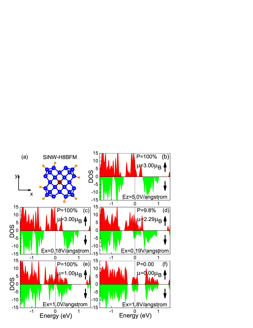
To examine whether the half-metallic property of the SiNW-H8BFM [Fig. 5(a)] is stable under external electric fields, we made calculations in presence of longitudinal and transverse electric fields, respectively. By applying an electric field along the nanowire direction (along axis), we found that the half-metallic behavior of the SiNW-H8BFM still retains under a field as large as 5.0 [Fig. 5(b)]. When an electric field is applied perpendicular to the nanowire axis (along direction), we observed that the half-metallic state is kept when the field is less than 0.18 [Fig. 5(c)]; when the transverse field reaches 0.19 [Fig. 5(d)] or larger, the spin polarization decreases dramatically, and the half-metallic property is destroyed, which becomes a FM metal. When the electric field increases further, say about 1.0 , the half-metallic property comes back again [Fig. 5(e)]. When the field exceeds 1.8 [Fig. 5(f)], it becomes a NM metal.
In summary, a novel type of half-metallic SiNWs along [100] direction by introducing multiple SDBs and boron doping is predicted by means of the spin-dependent ab initio calculations. The obtained results show that the half-metallicity in such SiNWs is quite robust against external electric fields. Under the circumstances with different SDBs, the H-passivated SiNWs can also be FM or AF semiconductors. The present findings might be applicable in nanospintronics and nanomagnetism.
The authors are grateful to X. Chen, S. S. Gong, X. L. Sheng, Z. C. Wang, and L. Z. Zhang for helpful discussions. The calculations are performed on the supercomputer NOVASCALE 6800 in Supercomputing Center of CAS. This work is supported in part by the NSFC (Grant No. 10625419), the MOST of China (Grant No. 2006CB601102), and CAS.
References
- (1) J. Appenzeller, J. Knoch, M. T. Björk, H. Riel, H. Schmid, and W. Riess, IEEE Trans. Electron Devices 55, 2827 (2008).
- (2) D. Wang, B. A. Sheriff, and J. R. Heath, Nano Lett. 6, 1096 (2006).
- (3) C. M. Lieber et al., Science 294, 1313 (2001).
- (4) Guo-Jun Zhang et al., Nano Lett. 8, 1066 (2008).
- (5) A. M. Morales and C. M. Lieber, Science 279, 208 (1998).
- (6) D. D. D. Ma et al., Science 299, 1874 (2003).
- (7) J. A. Yan, L. Yang, and M. Y. Chou, Phys. Rev. B 76, 115319 (2007).
- (8) E. Durgun, N. Akman, C. Ataca, and S. Ciraci, Phys. Rev. B 76, 245323 (2007).
- (9) A. K. Singh, V. Kumar, R. Note, and Y. Kawazoe, Nano Lett. 6, 920 (2006).
- (10) C. R. Leao, A. Fazzio, and A. J. R. da Silva, Nano Lett. 8, 1866 (2008).
- (11) R. Rurali and N. Lorente, Phys. Rev. Lett. 94, 026805 (2005).
- (12) R. Rurali, Phys. Rev. B 71, 205405 (2005).
- (13) S. Ismail-Beigi and T. Arias, Phys. Rev. B 57, 11923 (1998).
- (14) J. X. Cao, X. G. Gong, J. X. Zhong, and R. Q. Wu, Phys. Rev. Lett. 97, 136105 (2006).
- (15) E. Durgun, D. Cakir, N. Akman, and S. Ciraci, Phys. Rev. Lett. 99, 256806 (2007); E. Durgun, N. Akman, and S. Ciraci, Phys. Rev. B 78, 195116 (2008).
- (16) M.-V. Fernández-Serra, Ch. Adessi, and X. Blase, Nano Lett. 6, 2674 (2006).
- (17) H. Peelaers, B. Partoens, and F. M. Peeters, Nano Lett. 6, 2781 (2006).
- (18) R. Kagimura, R. W. Nunes, and H. Chacham, Phys. Rev. Lett. 98, 026801 (2007).
- (19) J. Cho and J. Choi, Phys. Rev. B 77, 075404 (2008).
- (20) S. Okada, K. Shiraishi, and A. Oshiyama, Phys. Rev. Lett. 90, 026803 (2003).
- (21) W. Kohn and L. J. Sham, Phys. Rev. 140, A1133 (1965).
- (22) J. P. Perdew, K. Burke, and M. Ernzerhof, Phys. Rev. Lett. 77, 3865 (1996).
- (23) N. Troullier and J. L. Martins, Phys. Rev. B 43, 1993 (1991).
- (24) P. Ordejón, E. Artacho, J. M. Soler, Phys. Rev. B 53, 10441 (1996).
- (25) Main properties have been confirmed in supercells of two and four units along z axis by SIESTA. We also used Quantum ESPESSO (P. Giannozzi et al., www.quantum-espresso.org) with plane wave basis sets and ultrasoft pseudopotentials to verify the relative energies of different spin configurations of SiNW-H8B in a unit cell, which gives similar results with SIESTA.