Formation of p-n junction in polymer electrolyte-top gated bilayer graphene transistor
Abstract
We show simultaneous p and n type carrier injection in bilayer graphene channel by varying the longitudinal bias across the channel and the top gate voltage. The top gate is applied electrochemically using solid polymer electrolyte and the gate capacitance is measured to be 1.5 , a value about 125 times higher than the conventional SiO2 back gate capacitance. Unlike the single layer graphene, the drain-source current does not saturate on varying the drain-source bias voltage. The energy gap opened between the valence and conduction bands using top and back gate geometry is estimated.
-
I Introduction
In recent years, single and a few layer graphene are at the center stage of intense research to unravel physical properties of these new forms of carbon, with an eye on device applications. Ultra high mobilities and observation of ballistic transport make graphene based devices a potential alternative for silicon based devices Novoselov 04 ; Novoselov Nat 05 ; Rise Nov ; Kim Suspended . The zero energy gap between the valence and conduction band in the energy spectrum of single layer graphene (SLG) makes it difficult to achieve a high on-off ratio in field effect transistor (FET). On the other hand, bilayer graphene (BLG) devices hold greater promise in terms of better device performance with larger on-off ratio. This is feasible because of the band gap opening due to the breaking of inversion symmetry of the two layers in an otherwise gapless energy band structure. Moreover, this gap between the conduction and valence band can be tuned by means of external gate electric field, as demonstrated both theoretically GeimBiased ; McannPRB(R) ; McannPRL ; CastroNetoReview ; MauriCondMat and experimentally OhtaScience ; Morpugo ; Atin ; NatureIR . In particular , Zhang et al. NatureIR have reported a direct observation of the band gap in the bilayer by infrared absorption. They have used dual gate bilayer FET where 80 nm Al2O3 film was used as the top gate and 285 nm SiO2 as the back gate.
Misewich et al.CNTScience have shown that it is possible to get polarized infrared optical emission from a carbon nanotube FET by creating an effective forward biased p-n junction along the nanotube channel. This was achieved by applying the gate-drain voltage VGD, comparable to the drain-source voltage VDS, and maximum emission was obtained when V. Electrical measurements showed that the optical emissions results from the radiative recombination of electrons and holes near the junction. Similar experiments carried out by Meric et. al. KimSaturation on single layer graphene (SLG) device have reported formation of p-n junction along the graphene channel. However, owing to the absence of the band gap in SLG, the recombination of electrons and holes at/near the junction does not yield any radiation. In comparison, bilayer graphene (BLG) device can serve as a prospective candidate is this regard since a band gap can be opened and controlled simultaneously by application of external electric field perpendicular to the layers. Thus, by creating a p-n junction along the bilayer channel by proper biasing of the device, we may be able to fabricate novel source of terahertz radiation TeraMag ; TeraJETP based on the recombination of carriers.
In this paper we show that the BLG device can change from unipolar state to ambipolar state by varying the drain-source bias along the bilayer channel at different top gate voltages (VT). This has been possible because of very high gate capacitance of the top gate. We also report a quantitative analysis of the band gap opening in the bilayer graphene energy spectrum. In order to control the gap and the position of the Fermi level independently, we have used the top and back gate device geometry. Solid polymer electrolyte and 300nm thick SiO2 were used as top gate and back gate materials, respectively. This top gate arrangement allows us to shift the Ferrmi energy significantly by applying a very small top gate voltage ( 1 V) because of its higher gate capacitance due to nanometer thick Debye layerAndyNature . In addition, our top gate geometry is a very simple way as compared to depositing high dielectric electric materials like HfO2 and Al2O3, using atomic layer deposition technique. We determine the top gate capacitance accurately by an application of top and back gates on a bilayer graphene device. It is shown that our device has very high gate capacitance , which is nearly 125 times larger compared to the gate capacitance of 300 nm SiO2 (12 ).
II Experiments and Results
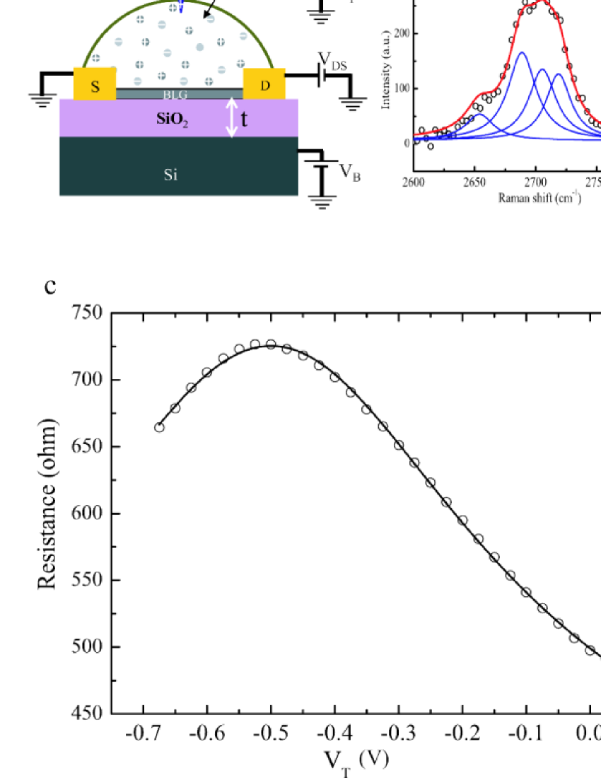
The device consists of bilayer graphene flake prepared from micromechanical cleavage of highly oriented pyrolytic graphite (HOPG) and deposited on Si/SiO2 substrate with the oxide thickness (t) of 300 nm. The electrical contacts on the bilayer device were made by e-beam lithography, followed by thermal evaporation of 30 nm of gold and subsequent liftoff in acetone. The source drain separation (L) is 500nm and the width (W) is 5m. All the measurements were done at room temperature using two probe contacts. The drain-source and both the top and back gate biases were given from Keithley 2400 source meters. The top gate material solid polymer electrolyte consists of LiClO4 and polyethylene oxide (PEO) in the ratio 0.12:1 AndyNature ; AndyPrb ; AndyCnt . The top gate voltage (VT) was applied by inserting a platinum electrode within the polymer layer. Figure 1(a) shows a schematic of the experimental set up. Raman spectroscopy using 514.5 nm excitation laser was used to identify the bilayer graphene (BLG) Ferrari fingerprint . Raman spectrum of the bilayer graphene with the 2D mode resolved into four peaks is shown in figure 1(b). Figure 1(c) shows the ambipolar nature of IDS as a function of VT for VDS = 10 mV and the back gate voltage VB = 0 V. The Dirac point is at V = -0.5 V, implying that our starting sample was electron doped. Mobility (), the minimum carrier concentration () and the total contact resistance (RC)are extracted by fitting the data to an equation based on diffusive transport model,
| (1) |
where RG is the resistance of the bilayer graphene, is the carrier density induced by the top gate and , and RC are the fitting parameters and the contact resistance (RC) is mainly at the source and drain contacts of the graphene and , arises mainly from charge puddles which are created due to charge impurities () 18 of KimSaturation ; 19 of KimSaturation lying between dielectric and the bilayer sample. In order to determine , we estimate the value of the top gate capacitance CT as follows.
II.1 Determination of polymer gate capacitance CT
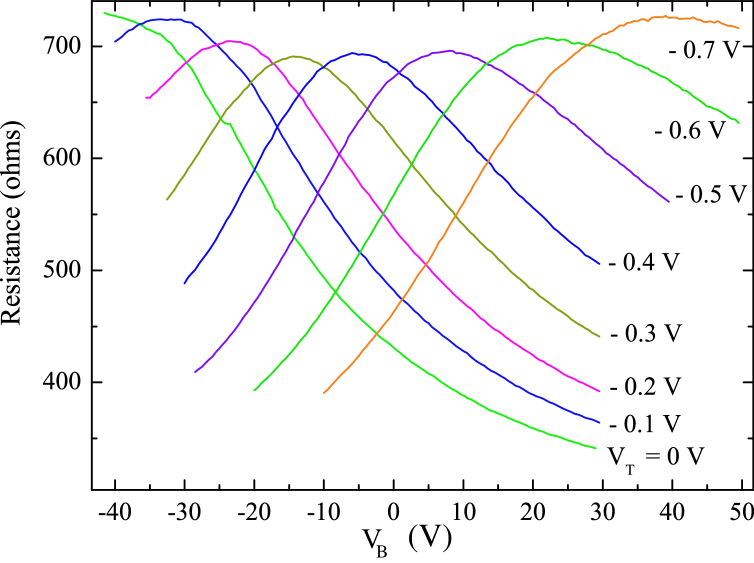
Figure 2 shows the resistance of the channel as a function of VB for a fixed VT. For a given gate voltage VG,
| (2) |
where is determined by the quantum capacitance of the bilayer and potential from the geometrical capacitance of the gateAndyNature ; AndyPrb . In equation (2), for top gate CG=CT, VG=VT, ; similarly for back gate CG=CB, VG=VB, . The gate-induced carrier density in a bilayer graphene is given by AndoBilayer ; AndyPrb
| (3) |
where is the inter-layer hopping energy ( 390 meV), and is the Fermi velocity = 10 Rise Nov . Therefore, for a given VT, the induced carrier density in the bilayer sample is
| (4) |
where
| (5) |
Similar expressions hold good for the back gate geometry and when resistance is maximum (Rm) at a back gate voltage , to make the Fermi energy shift zero. Therefore, for a given VT
| (6) |
where CT is the only unknown parameter. Using the known C and for different VT, the average value of CT is found to be . Note that, in this estimation the quantum capacitance is not assumed to be a constant as was done by Meric et. al.KimSaturation . Knowing CT, is thus determined as a function of VT from equation (4) and (5). The experimental curve of figure 1c is then fitted to equation (II) giving, = 730 cm2/V.sec, = 1.5 and RC = 150 .
II.2 Formation of p-n junction along the bilayer channel
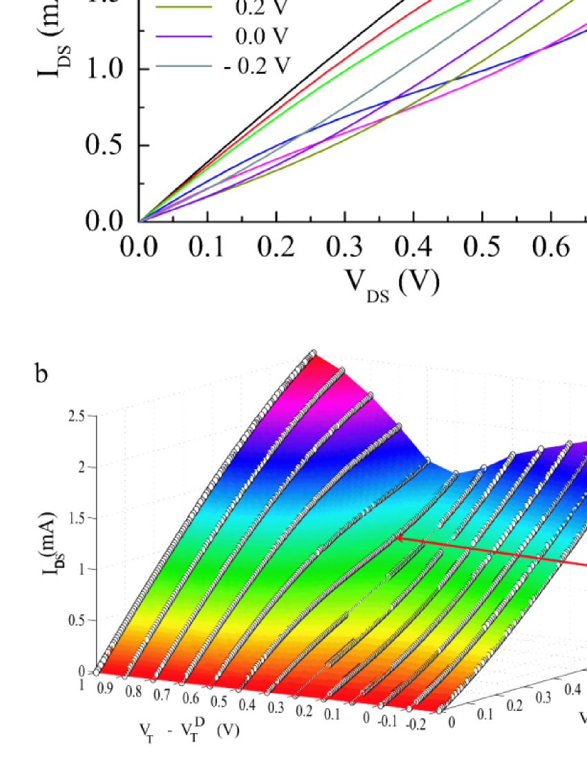
We now discuss the characteristics of drain-source current (IDS) as a function of drain-source bias (VDS). Figure 3(a) and b shows IDS vs VDS for different top gate voltages. The main noticeable feature is a clear non-linear dependence of IDS on VDS, and a significant effect of the gate voltage on the shape of the IDS - VDS curves.
To understand the non-linear IDS - VDS curve, we look at the schematic in figure 4(a). For VDS VT, the bilayer channel will be electron doped for (VT - V) 0 and hole doped for (VT - V) 0 and the doping () will be homogeneous along the channel length. However, this is not the case when VDS is comparable to VT. In this case the voltage difference between the gate and the bilayer channel varies from (VT - V) at the source to VDS - (VT - V) at the drain electrode. Therefore, by varying drain-source voltage (VDS) at fixed VT, the doping concentration changes from n type to p type along the channel length. In figure 4(a), we have shown the carrier distribution , along the bilayer channel for three different cases of drain-source voltage (VDS) at (VT - V) = 0.5 V.
Case 1: VDS (VT - V), and therefore the carriers will be electrons in the bilayer channel with = L). In this region, IDS increases sub linearly with VDS because the average carrier concentration [ = ] decreases with VDS.
Case 2: VDS = (VT - V), will be zero at = L and therefore, the conduction channel gets pinched off near the drain end making the region devoid of charge carriers. At this point the slope of the IDS vs VDS curve undergo a change (figure 4(b)).
Case 3: VDS (VT - V), the point in the channel where the pinch off occurs, moves deeper into the channel drifting towards the source electrode. As VDS (VT - V), the gate is negatively biased with respect to drain near the drain region. As a result carrier concentration will be holes near the drain region, as shown in the lower most panel of figure 4(a). When VDS is increased beyond pinch off, the current increases due to enhanced p channel conduction.
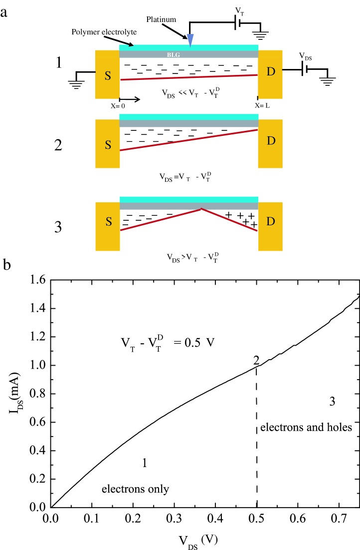
Thus the bilayer channel is now viewed as comprising of distinct electron and hole regions, with the electron doped region shrinking as the applied drain-source bias is increased. The potential drop across the electron channel remains fixed at VT - V while the drop across the hole region (from drain end to pinch off) increases as VDS - (VT - V), with the applied drain-source bias. As the device is operated beyond the pinch off, the dominant current carrier changes from electron to holes and the current increases as a function of VDS. It appears as if a forwrad biased p-n junction is formed at the pinch off region, with p-region towards the drain end and n-region to wards the source region.
A noticeable feature is the absence of current saturation in all the IDS vs VDS curves as compared to the monolayer case reported recently KimSaturation . In order to address if the small length of the channel in our experiment (500nm) is responsible for non-saturation of current KimSaturation ; CNTDrainScaling , we carried out experiments on a device of drain-source separation 2.5m and width 1.5 m. This also did not show any signature of current saturation.
In order to analyze the IDS - VDS curves, we model the drain ccurrent as
| (7) |
where D() is drift velocity. The drift velocity can be written as
| (8) |
where is the longitudinal electric field due to drain-source bias, V() is the potential drop at point in the channel and is the mobility. Therefore,
| (9) |
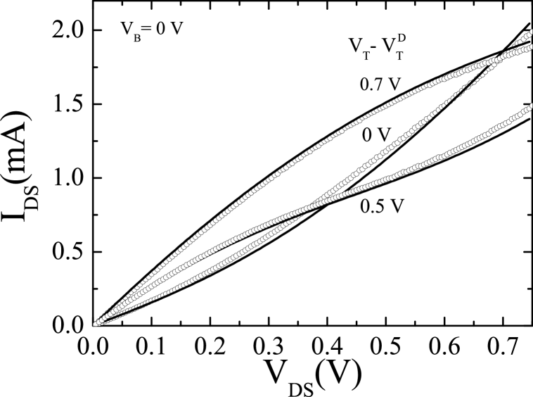
where the upper and lower limits signifies the voltage drop at the drain and source ends, respectively. The drop due to the contact resistance at both the ends has been assumed to be equal. Using the extracted values of the mobility (), the contact resistance (RC), n and , equation (9) is solved numerically. Figure 5 shows experimental data (open circles) for three top gate voltages along with the theoretical curves (solid lines). It can be noted that agreement between the experiment and the calculation is quite good.
II.3 Opening of energy gap in bilayer graphene and its estimation
Coming back to figure 2, it shows resistance as a function of the back gate voltage for a fixed top gate voltage. For VT = 0 V, the maximum value of resistance (Rm) at a negative back gate voltage (VV ) clearly establishes that the bilayer graphene channel is intrinsically n-doped. Figure 2 shows that the value of Rm is minimum at = -0.4 V and increases almost symmetrically on changing VT. It can also be seen, that for a particular top gate voltage, the drain-source current is not symmetric for electron and hole doping.
The change in the maximum value of resistance (Rm) at different top gate voltages arises due to the opening of an energy gap between the conduction and valence bands of the bilayer graphene GeimBiased ; OhtaScience ; Morpugo ; Atin ; NatureIR . It has been shown both theoreticallyMcannPRB(R) ; McannPRL ; CastroNetoReview and experimentally GeimBiased ; OhtaScience ; Morpugo ; Atin ; NatureIR that a difference between the on-site energy in the layers leads to an opening of the gap between conduction and valence band which touch each other at the zone edge K point of brillouin zone CastroNetoReview . This on-site energy difference can be controlled externally by the application of electric field, perpendicular to the layers, which implies a potential energy difference V and hence a gap . Experimentally such fields in-between two carbon layers were created either by application of top and bottom gates simultaneously Morpugo ; Atin ; NatureIR or by chemical doping of a back gated device GeimBiased ; OhtaScience . In the presence of an electric filed in between the layers, the Hamiltonian for the bilayer graphene near the K point can be written as
| (10) |
with, where and are the inplane and interlayer nearest neighbor hopping energies respectively. The eigen-values of the above Hamiltonian for the lower subbands of the bilayer graphene can be written as :
| (11) |
where correspond to conduction and valence bands, respectively. Figure 6(a) shows the band structure of bilayer graphene having a band gap (). The relation between the band gap and potential energy difference (V) is given by CastroNetoReview
| (12) |
which shows that there will be no band gap if V = 0.
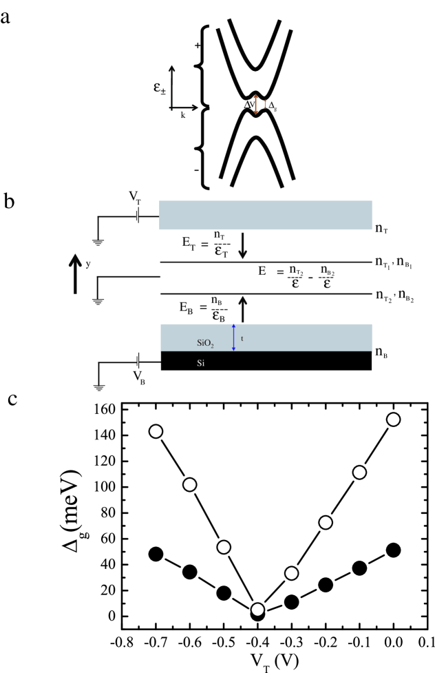
Figure 6(b) shows the induced carrier density in each carbon layer along with the electric field in between them in the presence of top and back gates. The total induced carrier density in bilayer, due to is: and similarly, for , . Therefore, total induced carrier density in bilayer graphene due to top and back gates is:
| (13) |
where, for simplicity, we have neglected the quantum capacitance . Considering the screened electric field , the induced carrier density due to top gate is and where subscripts 1 and 2 refer to top and bottom layers, respectively, as shown in figure 6(b). For a screening length of , we can write for top gate n where is the separation between the two layers (). Thus, for the top gate and . Similar expression holds good for the back gate. Thus, in presence of back and top gates the resultant electric field inside the bilayer would be , where
| (14) |
where 2.5 is the dielectric constant of the bilayer graphene CastroNetoReview .
The same analysis holds good for as well. Therefore, the net electric field between two carbon layers is,
| (15) |
It should be noted that for the equation (15) reduces to
| (16) |
i.e. the field without screening which corresponds to two layers having equal carrier density.
It can be seen from equation (13) and (15) that minimal value of the resistance maximum should appear when VB = 0 V and VT = 0 V, since this would imply that Fermi energy EF = 0 (since = 0) and band gap g = 0 (since E = 0). As mentioned earlier, in our experiment minimum value of Rm appears at VT = -0.4 V (figure 2) because of unintentional electron doping. To consider the effect of electric field inside the bilayer due to this unintentional electron doping, we place a positive charge sheet of carrier density above the top carbon layer, given by obtained from the back gate sweep for VT = 0 V, as shown in figure 2 (V -40V). Thus the net electric field inside the bilayer is written as
| (17) |
where is the field due to . The potential energy difference between the two layers is , and the value of the gap is estimated from equation (12). Taking back gate capacitance C and top gate capacitance C, figure 6c shows the plot of the value of the band gap, with screening Rise Nov and without screening , as a function of VT (where band gap values are evaluated at Rm for each of the back gate characteristic at fixed VT (figure 2)). It can be seen from figure 6c, that is minimum at VT = - 0.4 V. This trend follows from the trend of Rm (see figure 2). We notice that, had the arrangement of been placed below the bottom layer, then the field components associated with it would have changed their direction and the calculated energy gap would not have followed the trend of Rm. Thus, our assumption that the arrangement of unintentional carrier density lies above the top layer has indeed been justified
III Conclusions
In conclusion, the bilayer channel transforms from n type to p type conduction channel as we vary the drain-source voltage. This variation results in nonlinear dependence of IDS on VDS as a function of VT which has been quantitatively explained. Contrary to the recently reported monolayer case, we did not observe any signature of current saturation for IDS. In the presence of a gap in bilayer energy spectrum, the formation of p-n junction creates new possibility for the bilayer device as a source of terahertz radiation TeraMag ; TeraJETP , similar to infrared emission from the carbon nanotubes CNTScience . The radiation from recombination between electrons and holes at the junction may acts as terahertz source depending on the magnitude of the gap that can be opened. The opening of a gap in the bilayer spectrum was studied, where the gap was controlled using a top and back gate geometry. However the band gap opening is limited by the restriction on the back gate voltage, since the breakdown field for the SiO2 is 1V/nm ( up to 300V in our case). The capacitance of the polymer electrolyte was determined accurately. Thus solid polymer electrolyte gating of graphene devices may open up new avenues for graphene based electronics, particularly where higher carrier concentration is required.
Acknowledgements.
AKS thanks Department of Science and Technology for financial assistance through the DST Nanoscience Initiative Project.References
References
- (1) Novoselov K S, Geim A K, Morozov S V, Jiang D, Zhang Y, Dubonos S V, Grigorieva I V and Firozov A A 2004 Science 306 666-669
- (2) Novoselov K S, Geim A K, Morozov S V, Jiang D, Katnelson M I, Grigorieva I V, Dubonos S V, and Firozov A A 2005 Nature 438 197-200
- (3) Geim A K, and Novoselov K S 2007 Nature Materials 6 183-191
- (4) Bolotin K I, Sikes K J, Stormer H L and Kim P 2008 Phys. Rev. Lett. 101 096802
- (5) Castro E V, Novoselov K S, Morozov S V, Peres N M R, Lopes dos Santos J M B, Nilsson J, Guinea F, Geim A K and Castro Neto A H 2007 Phys. Rev. Lett. 99 216802
- (6) McCann E, 2006 Phys. Rev. B 74 161403(R)
- (7) McCann E and Falko V I 2006 Phys. Rev. Lett. 96 086805
- (8) Castro E V, Novoselov K S, Morozov S V, Nilsson J, Guinea F, Geim A K and author Castro Neto A H e-print arXiv:cond-mat/0807.3348v1
- (9) Gava P, Lazzeri M, Saitta A M and Mauri F e-print arXiv:cond-mat/0902.4615v1
- (10) Ohta T, Bostwick A, Seyller T, Horn K and Rotenberg E 2006 Science 313 951-954
- (11) Ostinga J B, Heersche H B, Liu X and Morpugo A F 2008 Nature Materials 7 151-157
- (12) Pal A N and Ghosh A 2009 Phys. Rev. Lett. 102 126805
- (13) Zhang Y, Tang T, Girit C, Hao Z, Martin M C, Zettl A, Crommie M F, Shen Y R, Wang F 2009 Nature 459 820-823
- (14) Misewich J A, Martel R, Avouris Ph, Tsang J. C, Heinze S and J. Tersoff 2003 Science 300 783-786
- (15) Meric I, Han M Y, Young A F, Ozyilmaz B, Kim P and Shepard K L 2008 Nature Nanotechnology 3 654-659
- (16) Berman O L, Gumbs G and Lozovik Y E 2008 Phys. Rev. B 78 085401
- (17) Aleshkin V Y, Dubinov A A and Ryzhii V 2009 JETP Letters 89 63-67
- (18) Das A, Pisana S, Chakraborty B, Piscanec S, Saha S K, Waghmare U V, Novoselov K S, Krishnamurthy H R, Geim A K, Ferrari A C and Sood A K 2008 Nature Nanotechnology 3 210-215
- (19) Das A, Chakraborty B, Pisana S, Piscanec S, Sood A K and Ferrari A C 2009 Phys. Rev. B 79 155417
- (20) Das A, Sood A K, Govindaraj A, Saitta A M, Lazzeri M, Mauri F and Rao C N R 2007 Phy. Rev. Lett. 99 136803
- (21) Ferrari A C, Meyer J C, Scardaci V, Casiraghi C, Lazzeri M, Mauri F, Piscanec S, Jiang D, Novoselov K S, Roth S and Geim A K 2006 Phys. Rev. Lett. 97 187401
- (22) Adam S, Hwang E H, Galitski V M and Sharma S D 2007 Proc. Natl. Acad. Sci. USA 104 18392-18397
- (23) Martin J, Akerman N, Ulbricht G, Lohmann T, Smet J H, von Klitzing K and Yacoby A 2008 Nature Physics 4 144-148
- (24) Ando T 2007 J. Phys. Soc. Jpn 76 104711
- (25) Radosavljevic M, Heinze S, Tersoff J, and Avouris Ph 2008 Appl. Phys. Lett. 83 2435-2437