Spatial Distribution of the Incompressible Strips at Aharonov-Bohm Interferometer
Abstract
In this work, the edge physics of an Aharonov-Bohm interferometer (ABI) defined on a two dimensional electron gas, subject to strong perpendicular magnetic field , is investigated. We solve the three dimensional Poisson equation using numerical techniques starting from the crystal growth parameters and surface image of the sample. The potential profiles of etched and gate defined geometries are compared and it is found that the etching yields a steeper landscape. The spatial distribution of the incompressible strips is investigated as a function of the gate voltage and applied magnetic field, where the imposed current is confined to. AB interference is investigated due to scattering processes between two incompressible ”edge-states”.
keywords:
Aharonov-Bohm interferometer , Quantum dots , Screening , Double-Slit experiments , Phase lapsesPACS:
73.20.Dx, 73.40.Hm, 73.50.-h, 73.61,-rThe recent increasing interest towards the quantum Hall based interferometers relies on the popularity of the quantum information processing. In particular, the realization of electron and quasi-particle interference experiments became a paradigm [1, 2]. A possible application is proposed to use the non-Abelian 5/2 state for topological quantum computation [3], which essentially has a very similar structure of AB interferometers. The well established experimental wisdom is that, to realize ”clean” measurements are extremely difficult, which strongly depends on the sample geometry, crystal growth etc. In typical AB interference experiments two propagating states are brought to close vicinity, by the help of gates [1]. The edge states form a closed (or almost closed) path, which enclosures certain amount of magnetic flux. By changing the magnetic field or the area of the closed path, one infers the phase of the particles. The conventional edge picture is used to explain the observed AB oscillations [4], however, the actual distribution of the edge-states is still not known for realistic samples, although, several powerful techniques are used [5]. At the recent experiments of Camino et. al [2], show that the conventional AB theories, which neglect electron-electron interactions, are unable to explain the periodicity of the oscillations. The only very recent model of Igor Zozoulenko [5] could provide a reasonable explanation for the unexpected behavior, which states that ”standard transport models” fail to understand the underlying physics. However, the model geometry considered in their work is quite different from the actual experimental setup. Here, we provide an explicit calculation scheme to obtain the density and potential profiles of an AB interferometer in the absence of an external magnetic field and also under quantized Hall conditions. Our calculation is based on solving the Poisson equation in 3D, starting from the crystal growth parameters and the lithographically defined surface patterns. A fourth order nearest neighbor approximation is used on a square grid with open boundary conditions and 3D fast Fourier transformation method is used to obtain the solution iteratively [6, 7]. The outcome, i.e. the potential and electron density distributions, of this calculation is used as an initial condition for the magnetic field dependent calculations. The distinguishing part of our calculation is that we do not have to assume only gate defined structures but we can also handle etching defined geometries, which essentially is the case for the experiments. We show that, the etching defined samples present a sharper potential profile [7], therefore, the formation of the edge-states are strongly influenced. This, obviously, effects the edge physics in determining the AB oscillations.
The simple description of an ABI, is such: let us assume a closed path, a circle for simplicity, subject to a perpendicular magnetic field with an area of where is the radius. Since the wave function travelling from one side should be the same as the one the travelling from the other side, the phase difference of the wave functions can be only integer multiples of the magnetic flux quanta encircled. In other words, for a given flux every spin resolved cyclotron orbit should satisfy the condition , where is the quantum number of the orbit. Therefore, an orbit with a radius of magnetic length will have an area , resulting in . It is common to define the occupation of these orbits by , where is the number of the electrons and this occupation is called the filling factor. This picture should also hold for non-interacting electrons which are confined by an external potential , which essentially lifts the degeneracy. In the experiments considered in this work, it was shown that the number of electrons is fixed (, varying with the sample size) in the ”island”, which means that it is energetically almost impossible to add or subtract an electron from the quantum dot region. If one keeps the electron density fixed and decreases the field by a factor of two, the filling factor increases by a factor of two, which implies that the are enclosed by is now half.
In this work we only consider the ABI experiments conducted at the integer quantize Hall regime, i.e. and [1] and the results reported in Ref.[2] at the integer regime. The first work concentrates the AB oscillations observed only at the plateau. In the above mentioned experiments, the magnetic field and the front gate dependency of the AB period is investigated and the results are discussed in terms of the Gelfand and Halperin (GH) [8] and Chklovskii, Shklovskii and Glazman (CSG) [4] edge models. A hybrid formula is then used to describe the actual electron density distribution non-self-consistently. Procedure is as follows: The GH model describes (almost) properly the etched edge density profile and CSG model provides a dependency. Therefore, the density distribution without gates is taken from the GH model and its evolution depending on the front gate bias is described by the CSG model. It is argued that, this hybrid model is in agreement with the experiments with a difference of when comparing the surface area change of a single edge-channel at the gap as a function of . Such a relatively small difference, at a first glance, looks impressive. However, in the second report [2], where the results at is also shown, it was stated that if the radius of the outer ring remains unchanged the AB oscillations can be explained.
Our investigation is based on the calculation of the electron density and screened potential self consistently within the Thomas-Fermi approximation (TFA) [7]. We consider spinless electrons in the high magnetic field regime, consequently the effective Hamiltonian reads,
| (1) |
Here is the kinetic part, and are the external and interaction potentials, respectively. The external potential is obtained by the above mentioned 3D calculations considering the real experimental structure, whereas the interaction potential (Hartree potential) is calculated for a given density, boundary conditions and gate pattern by solving the Poisson equation
| (2) |
where is the dielectric constant ( for GaAs). The Kernel is the solution of the Poisson equation preserving the periodic boundary conditions. Spatial distribution of the electron density is obtained within the TFA via,
| (3) |
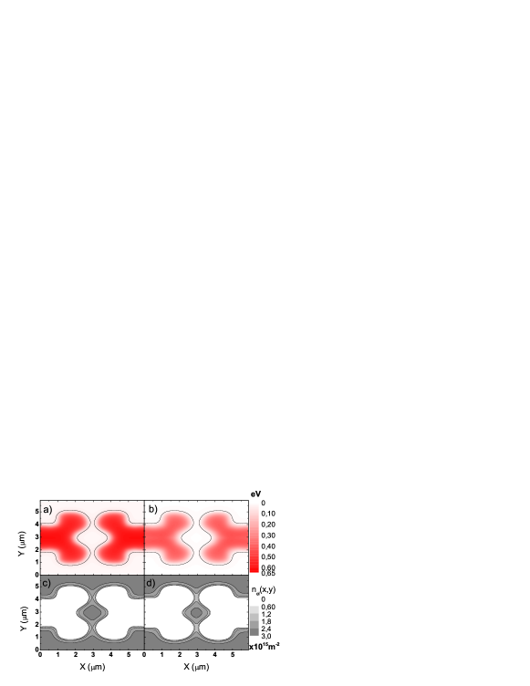
where is the relevant (collision broadened) density of states, determines the particle statistics (Fermi function) and is the electrochemical potential. The total potential and eq. 3 are calculated self-consistently to obtain the electron and potential distributions at finite magnetic field and temperature. We first compare the results of the gate and trench gate defined samples. We show the potential profiles and electron distributions both of these samples in Fig. 1, the upper panels illustrate the potential profiles and it is seen that the trench gate defined sample has a sharper profile. Fig 1c and fig. 1d represent the electron densities with gray scale, calculated for two different definitions. These results are obtained at zero magnetic field and temperature as an initial condition for our non-zero magnetic field calculation. The maxima of the electron density at the center of the q-dot matches perfectly () with the experimental value when considering the trench gated numerical simulation.
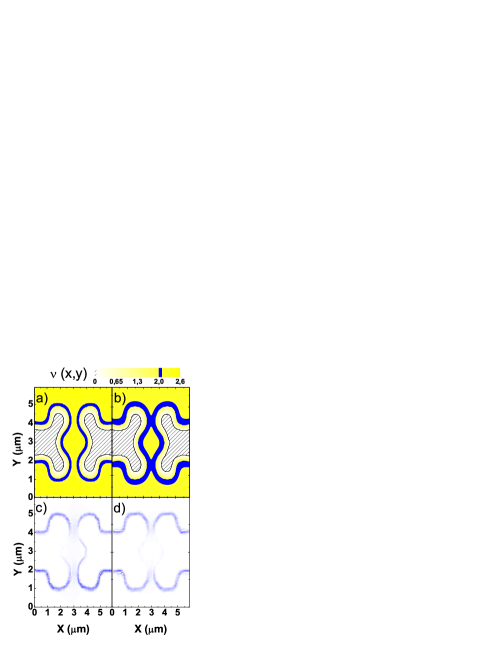
Next we calculate the potential and electron density distribution at finite temperature and field, only considering the trench gated sample. In Fig. 2 we show the spatial distribution of the ISs at two different magnetic field values. Shaded areas indicate that the electrons on the 2DEG are depleted perfectly. The side-surface electrons which exists on the side surface due to etching, yield larger shaded regions than the only gated model. Since the potential is sharper at trench-gated defined samples the widths of the incompressible strips are narrower compared to gated samples. When considering the field regime there is only a narrow interval where two incompressible strips are close to each other fig. 2a, however, do NOT merge 2b. Fig. 2c and fig. 2d presents the corresponding calculated current distribution utilizing the local Ohm’s law [9, 10, 7]. We clearly observe that, the imposed fixed current is confined within the incompressible regions, where backscattering is absent. It is known that the current flowing from the incompressible strips is divergent free, thus it is not possible to inject current directly to these strips. Hence, without scattering between two ”edge channels” one would not be able to observe any interference pattern. The scattering mechanism comes from the impurities or the electric field at the boundary between the ISs and compressible region [11], which we implicitly include to our calculations when calculating the local conductivity tensor elements using the findings of self-consistent Born approximation [10].
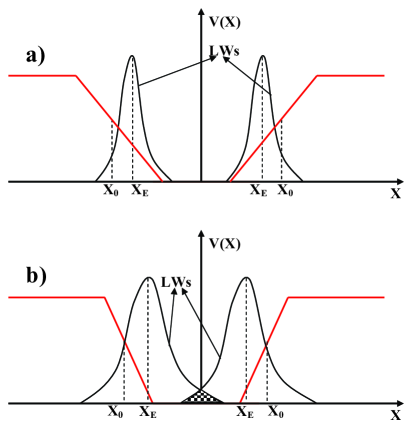
We aim to investigate a situation where, the spin-degenerate groun state Landau wave functions (LWs) overlap at a certain spatial region where scattering matrix elements become finite, hence we can observe the Aharonov-Bohm interference (ABI). Since the screening is merely poor within the ISs, the total potential exhibits a variation where the electron density is constant [12]. Therefore an electric field develops within this regions if we have a slope on the potential profile, that can be computed from . Using this equation and considering the calculated total potential profile on can obtain the spatial shift, , of the center coordinates of the LWs from
| (4) |
note that the LWs remain unaffected (i.e a Gaussian centered at ) in the compressible regions, since the potential is (almost) constant. Now, if the ISs are large and sufficiently far apart, no scattering processes can take place hence no interference can be observed. Such a case is shown in fig. 3a. Whereas, if the two incompressible edge states are close enough to each other and is large and LWs overlap, i.e. scattering takes place. This is shown in Fig. 3b. If we apply a high magnetic field ISs become broaden contrarily take small values so the shift of the center coordinate is negligible and as a result no overlap occurs. Since the widths of the incompressible strips are related to the pattern geometry and crystal growth parameters, the observation of AB interference patterns are extremely fragile. For such experiments, one should design the sample geometry and choose the magnetic field interval keeping in mind that the formation and the spatial distribution of the incompressible strips are important. The calculation of the actual scattering matrix elements for the real structures considering self-consistently calculated wave functions is beyond the scope of the present paper. However, we have drawn the calculation scheme.
To summarize: We have calculated self-consistently the electron and potential distribution considering the experimental sample geometry and material properties. It is shown from the 3D calculations that, the trench gated structure can be simulated in a fairly good agreement (with error). In the second part of our work we have also considered the interference conditions depending on the magnetic field value and observed that the scattering from one edge to the other is only possible if the two incompressible strips are close enough, i.e. at the order of magnetic length. If the two ”edge states” merge no partition takes place, hence interference pattern is smeared.
We would like to thank V. J. Goldman for fruitful discussions and providing us the sample details. The Feza-Gürsey Institute is acknowledged for organizing the III. Nano-electronics symposium. This work was supported by the Scientific and Technical Research Council of Turkey (TUBITAK) for supporting under grant no 109T083.
References
- [1] F. E. Camino, et.al, Phys. Rev B (72) (2005) 155313.
- [2] F. E. Camino, et.al, Phys. Rev. Lett. 98 (7) (2007) 076805.
- [3] S. Das Sarma, et.al, Phys. Rev. Lett. 94 (16) (2005) 166802.
- [4] D. B. Chklovskii, et.al, Phys. Rev. B (46) (1992) 4026.
- [5] S. Ihnatsenka, et.al, [cond-mat/mes-Hall 0803.4303].
- [6] A. Weichselbaum, et.al, Phys. Rev. E 68 (5) (2003) 056707.
- [7] S. Arslan, et.al, Phys. Rev. B 78 (12) (2008) 125423.
- [8] B. Y. Gelfand, et.al, Phys. Rev. B (49) (1994) 1862.
- [9] K. Güven, et.al, Phys. Rev. B (67) (2003) 115327.
- [10] A. Siddiki, et.al Phys. Rev. B (70) (2004) 195335.
- [11] A. Siddiki, EPL (87) (2009) 17008–17014.
- [12] A. Siddiki, et.al, Phys. Rev. B (68) (2003) 125315.