Atom lithography without laser cooling
Abstract
Using direct-write atom lithography, Fe nanolines are deposited with a
pitch of 186 nm, a full width at half maximum (FWHM) of 50 nm, and a height
of up to 6 nm. These values are achieved by relying on geometrical
collimation of the atomic beam, thus without using laser collimation
techniques. This opens the way for applying direct-write atom lithography to
a wide variety of elements.
PACS 81.16.Ta; 37.10.Vz; 3.75.Be
1 Introduction
In direct-write atom lithography, also known as laser-focused deposition, atoms are focused into a periodic pattern by a standing light wave. This technique has been applied to Na art1 , Cr art2a ; art2b , Al art3 , Yb art4 , and Fe art5 ; art6 . Just as for the case of focusing light, a well collimated atomic beam is crucial for atom lithography. An atomic beam arriving at the lens with a local angular spread (see Fig. 1) will result in broadening of the deposited features. To obtain a well collimated atomic beam, laser cooling techniques are generally used. However, effective laser cooling requires a closed optical transition. For numerous elements a closed transition is not accessible with present lasers, or hyperfine splitting is present, and the use of several repumping lasers becomes a necessity. For Fe, for instance, an accessible closed transition from the ground state does not exist, resulting in the loss of focusable atoms when applying laser cooling art8 .

It is because of these drawbacks that we decided to laser focus Fe without the use of any laser collimation techniques, simply relying for this part on geometrical collimation. We will show that in this way periodic grids of Fe nanolines with a FWHM of 50 nm, a height of up to 6 nm, and a period of 186 nm can still be deposited. Thus, we prove that atoms can be focused without using laser collimation. This makes the technique suitable for direct-write atom lithography of any species with transitions of sufficient strength that are not necessarily closed. Especially for atom lithography of technologically relevant elements such as Ga art9 , In art10 ; Kloeter2008 , and Si art11 , for which laser collimation imposes large experimental difficulties, this is a step forward. Also, laser focusing of molecules may be feasible this way.
For an earlier review of both direct-write and resist-based atom lithography, see Ref. Meschede2003 .
As the experiments are time-consuming, it is important to choose the experimental parameters carefully a priori. This is facilitated by the availability of an efficient and realistic simulation procedure for the atomic trajectories. Also, a comparison with simulations is essential for the careful analysis of the experimental results. We use a fast semiclassical Monte-Carlo procedure based on the dressed state model art13 that includes the effects of diffusion induced by spontaneous emission as well as of non-adiabatic transitions between dressed states.
In Sect. 2 our procedure for simulating standing-wave laser focusing is described in more detail. In Sect. 3 the experimental setup is described. The experimental results of atom lithography without laser collimation are compared with the outcome of the simulations in Sect. 4, followed by the conclusions in Sect. 5.
2 Simulations
Our simulation is based on the dressed state model introduced by Dalibard and Cohen-Tannoudji art13 . In this model one considers the eigenstates of the complete atom plus laser light field system. The energies of these states are given by:
| (1) |
with the number of photons in the light field, the frequency of the light field, the detuning of the light field from the atomic resonance . The frequency separation between the dressed states is given by:
| (2) |
with the Rabi-freqency, where represents the natural linewidth, the light intensity, and the saturation intensity. The dressed states are a linear superposition of the ground and excited states:
| (3) |
Here is defined by:
| (4) |
In our simulation, atoms move as classical point particles in a potential field given by the dressed-state energy shift , where the sign indicates the dressed state the system is currently in. The light mask is described as a one-dimensional Gaussian standing wave along the -axis with a waist and maximum on-axis intensity :
| (5) |
Here is the wavenumber of the light and the propagation direction of the atoms is assumed to be along the -axis. As the atoms’ kinetic energy is much larger than the potential height of the light mask we can neglect its effect on the longitudinal motion, so that the atom’s motion is described by a one-dimensional Newtonian equation of motion in the -direction, which is solved numerically.
Outside the standing wave the intensity of the light is zero and the ground state is for and for . Unless the atoms undergo a spontaneous or non-adiabatic transition, they will stay in their initial state.
The effects of spontaneous emission, and hence diffusion in the atom’s motion, are included in the model by evaluating the probability that an atom has undergone spontaneous emission at regular time intervals. By far the largest contribution to the diffusion is caused by emissions that change the sign of the dressed state, causing an instant reversal of the force on the atom. The relevant transition rates are given by:
| (6) | |||
| (7) |
with defined in Eq. 4. The probability of a dressed state transition due to spontaneous emission is given by or , depending on the initial dressed state, with the time interval.
Non-adiabatic transitions can occur when the atom moves too fast, or in other words, the eigenstates (dressed states) change too fast for the internal state of the atom to follow. The atom is then transferred from one dressed state to the other. This is most likely to occur when atoms cross a node of the standing wave. Non-adiabatic transfer is incorporated in the simulation procedure, but does not contribute significantly for present experimental conditions.
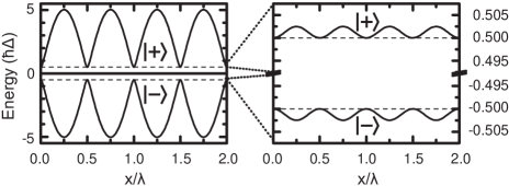
Before we show the results of these semiclassical simulations, we discuss the potential that is used. The left part of Fig. 2 displays the potential for the case of a strong light field, where . The case of a weak light field with is displayed to the right. Both potentials are very different in shape.
In the strong field limit, the potential minima of the state differ radically in shape from those of the state. The minima of the state are smooth, broad and parabolic over a large range around the minima. Using such a potential is a way to avoid non-parabolic aberrations in the atom focusing process. On the other hand, the minima of the state look like a V-shaped potential. The oscillation period of the atoms in the potential then depends on the starting point of the oscillation, leading to strong aberration in the focussing. The optical equivalent of such a lens is a conical lens or axicon. The aberration leads to a less sharply defined focus with a long focal depth, or a focal line.
For positive detuning, the atoms start out in the state and are subject to the V-shaped potential. Provided that they do not switch between dressed states due to spontaneous emission, this then creates focal lines – aligned with the nodes – rather than focal points. Hence, the formation of structures should be fairly insensitive to the experimental parameters. For negative detuning, the situation is reversed and the atoms are focussed by the smooth potential, in principle creating sharper focal points – aligned with the antinodes – because of the reduced non-parabolic aberration. However, these focal points are subject to severe abberation caused by the spread in longitudinal velocity, the atom-optical equivalent of chromatic aberration. This negates the advantage of the reduced non-parabolic aberration.
The potential for a weak standing wave is sine-like. The difference in shape between the and state minima has vanished, and focusing is expected to proceed in a similar fashion for both states.
The experiments and simulations described here have all been performed in the strong field case, with typical maximum values of , with both positive and negative detuning.
For the experiment, the 5DF5 atomic transition of iron is used. The wavelength is 372 nm. The isotope 56Fe has a natural abundance of 91.8%, of which at a typical evaporation temperature of 2000 K 50% is still in the 5D4 ground state. Hyperfine structure is absent in 56Fe. For this transition, and the saturation intensity for the magnetic subtransition is . The light mask is a one dimensional standing light wave produced by an elliptical Gaussian beam with waist radius along the atomic beam axis and perpendicular to it.
For the calculation, we start with 10,000 atoms. Each atom is initially assumed to be in a random magnetic substate. The saturation intensity is then calculated using the appropriate Clebsch-Gordan coefficient for the substate and laser polarization. Spatially, the atoms are homogeneously distributed over a single wavelength in the -direction.
The longitudinal velocity distribution of the atomic beam is that of an effusive beam, i.e., a Maxwell-Boltzmann distribution with average velocity . The transverse velocity distribution of the atoms is determined by the longitudinal velocity and the geometrical collimation. The beam divergence, emerging from a round nozzle with diameter at a distance from the standing wave, is characterized in good approximation by a Gaussian angular distribution with a root-mean-square (RMS) width of . This leads to a Gaussian transverse velocity distribution with an RMS spread of .
The equation of motion of every atom is integrated over a set time interval, before we check for spontaneous and non-adiabatic transitions. The effect of both transitions is to change from one dressed state to the other. The possibility that atoms, which undergo a spontaneous emission, decay to a different magnetic substate, is neglected.
The integration starts when the atom’s longitudinal position () is three times the waist radius of the Gaussian laser beam before the center of the laser beam, and ends at the same distance after the center. We make a histogram of the atomic flux distribution at set longitudinal positions.
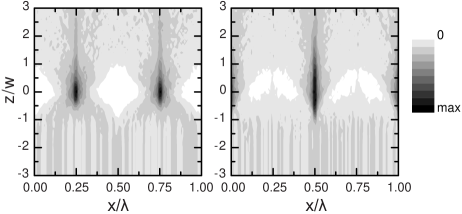
To demonstrate the difference in focusing between the negative and positive detuning, we first simulate focusing of a perfectly collimated atom beam, setting the RMS spread in transverse velocity to zero. A round laser beam with , a power of and linear polarization is taken. The detuning of the light with respect to the atomic transition is set at (2) MHz (58 ). These parameters lead to a maximum value of The results are shown in Fig. 3. Interaction with a red-detuned standing wave generates focal points, as shown on the left. The blue-detuned standing wave gives rise to focal lines, as shown on the right. For blue detuning, the atoms experience on average 0.45 dressed state-changing spontaneous emissions occur. For red detuning, the average number of emissions is 0.7, reflecting the fact that atoms are attracted to intensity maxima in this case, where the absorption rate is higher.
The strength of the lenses varies per atom. This is due primarily to the distribution over the magnetic substates of the Fe atoms; secondarily, the longitudinal velocity spread of the Fe atoms also contributes. The relatively long -range over which atom focusing occurs for the blue detuned case stands out.
3 Experimental setup
An Fe atomic beam is produced using an Al2O3 crucible with a nozzle diameter of 1 mm heated to a temperature of around 2000 K by a carbon spiral heater art16 , resulting in a typical Fe density in the source of m-3. At this temperature the Fe-beam intensity is s-1sr-1, and the average longitudinal velocity .
The 372 nm light needed to excite the 5DF5 transition is produced by a titanium-sapphire laser, frequency doubled with an LBO-crystal in a ring cavity. This laser system is locked to the transition using a hollow cathode discharge cell, described in art17 . An Acousto-Optical Modulator (AOM) is used to introduce the detuning of ) MHz between the light and the atomic resonance.
The Fe atoms are deposited on a native oxide Si[100] substrate, 650 mm downstream from the nozzle. With the 1 mm nozzle hole diameter, the divergence of the Fe beam therefore amounts to RMS and the spread in transverse velocity to RMS. The divergence is thus considerably larger than the best value obtained in our earlier experiments with transverse laser cooling of Fe art8 (). However, the divergence does not yet limit the obtained width of the deposited nanolines, which is equal to the width obtained with the lasercollimated beam art5 .
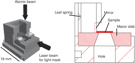
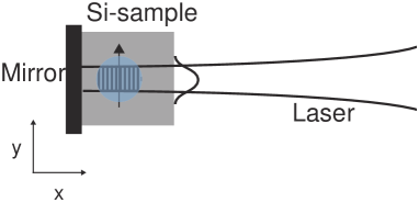
The Si samples can be 3 to 8 mm wide and 2 to 10 mm long. The Si sample is clamped on a compact sample holder (Fig. 4), on which also an mm mirror is mounted. These sample holders can easily be removed from the deposition chamber and stored in a load lock by a magnetic translator so that the alignment of sample and mirror, which have to be perpendicular to each other within 1 mrad, can be done ex vacuo. The pressure in the deposition chamber is typically mbar.
To create the standing light wave, the laser beam is focused to a waist of 50 m parallel to the atomic beam and 80 m perpendicular to the atomic beam, located at the surface of the sample holder mirror. The light is linearly polarized.
The substrate is positioned close to the center of the laser beam. Experiments have been performed with the substrate at the center of the waist, thus cutting the laser beam in half, as well as with the substrate positioned at the rear end of the laser beam waist, such that just 10% of the power in the laser beam is cut off by the substrate. Both cases are schematically drawn in Fig. 5.
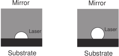
According to the simulations, the 50% cut-off configuration should lead to somewhat narrower focussed lines and results that are less sensitive to variations in laser power. However, diffraction effects, which are difficult to take into account in the calculations, are more serious than in the 10% cut-off case.
To prevent Fe from oxidizing, a Ag capping layer of approximately 5 nm is deposited using an effusive source operated at a typical temperature of 1140 K, resulting in a deposition rate of 0.15 nm/min.
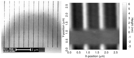
Although the height of the deposited structures can be easily measured by an AFM microscope, in order to determine the average thickness of the deposited Fe layer as well (and hence the thickness of the background layer) we need to calibrate the overall Fe deposition rate. To achieve this, we first produce structures by depositing Fe through a mechanical mask. The mask is made by e-beam lithography of a SiN membrane. Lines have been etched in the membrane with a width of about 150 nm and a period of 744 nm over an area of 250 250 m. The mask is pressed onto the substrate with a metal foil of 100 m as spacer between the bottom of the mask and the front of the substrate. Deposition through such a mask results in background-free nanolines, and thus gives a direct measurement of the total deposited layer thickness. A SEM-scan of the mask and an AFM-scan of the Fe-lines grown through the mask are shown in Fig. 6. The FWHM width of the structures is about 150 nm. From the height of the deposited structures the deposition rate is measured. The measured deposition rate varies between 3 and 7 nm/hour, depending on the exact temperature and filling of the crucible. In the evaluation of the deposited structures, the calibration of the deposition rate has been performed under conditions as close to the specific deposition experiment as possible.
4 Results
We have deposited nanoline arrays of Fe with both negative and positive detuning of the light and with substrates positioned both at 50% cut-off and at 10% cut-off. The dependence on the light intensity of the height and width of the nanolines has been investigated, as well as the ratio of line height to the average layer thickness. Since we have an AOM with a fixed RF-frequency of 150(2) MHz, our measurements are limited to blue and red detuned focusing at this frequency shift from resonance.
On each deposited sample, the height and width of the nanolines has been measured as a function of position transverse to the laser beam axis (i.e., along the -axis). Fig. 7 depicts the geometry. As the laser beam has a Gaussian profile, each -position is characterized by a different light intensity.
In Fig. 8 a 4 m AFM scan of a typical sample after deposition is shown. In 2 hours deposition time we grow structures up to heights of 6 nm. Fig. 9 shows a cross section through the scan over a range of . The distance between consecutive lines (the pitch of the modulation) is equal to =186 nm.
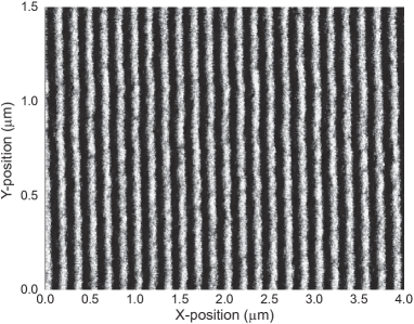
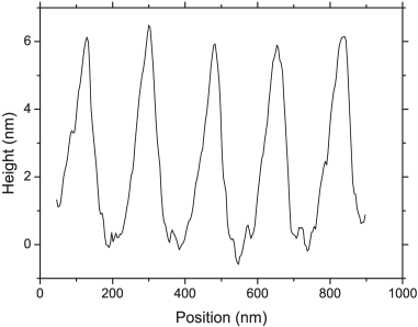
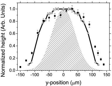
Fig. 10 shows a typical profile of the height of the nanolines as a function of transverse position. The intensity profile of the laser beam is shown as well. For high intensities, the height of the nanolines is largely independent on the light intensity both in experiment and simulation: the height profile does not follow the Gaussian shaped laser intensity profile, but it has a broad flat top. The height of the potential shown in Fig. 2 follows, in the high intensity limit, from the square-root of the intensity. Increasing the intensity will move the focus over the point towards negative -values. Since the lens, especially in the blue detuned case, has a large focal depth, the atoms remain focused at the position, even for higher intensities, resulting in the flat top of the height profile.
The results of the simulations are shown as well in Fig. 10. Both curves are normalized to the same height. The agreement between the experimental data and the results of the simulations is good when we look at the shape of the profile. At low intensities, the measurements deviate somewhat from the simulations. This may be caused by the non-Gaussian tails in the spatial profile of the laser beam used in the experiment.
Experimental data and simulation results on the width of the structures as function of the position on the substrate are shown in Fig. 11.
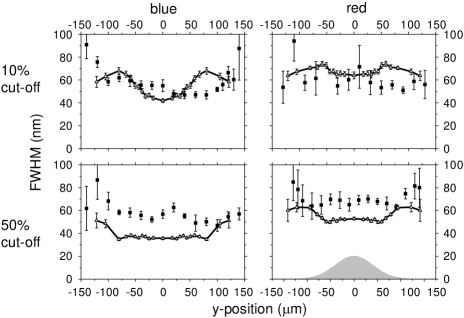
For high intensities, blue detuning results in slightly narrower lines compared to red detuning in the experiment. This difference is more pronounced in the simulations, and results from different focusing potentials (Fig. 2). The match between measured and simulated widths is better in the 10% cut-off configuration than in the 50% cut-off configuration. Diffraction of the laser beam is not included in the simulation. This may result in an underestimate of the nanoline widths in the 50% cut-off simulation.
Determining the ratio of the height of the nanolines to the average thickness of the Fe layer requires the calibration of the overall deposition rate as discussed in Section 3. Although this calibration is not very accurate, the result is that in our experiment the ratio for all experimental conditions is approximately 0.5 for the lines at maximum laser intensity (the center of the height profile as shown in Fig. 10).
| red | blue | |
|---|---|---|
| 50% cut-off | 1.25 | 1.25 |
| 10% cut-off | 0.60 | 0.70 |
To obtain the same ratio from the simulations we assume that 50% of the atoms are in the 5D4 ground state, which is the thermal occupation of the ground state at a source temperature of 2000 K. The other 50% of the 56Fe atoms, as well as the other isotopes, are not affected by the focusing light field and only contribute to the background layer. In Table 1 the ratio between simulated line heights and the average Fe layer thickness at maximum laser intensity is listed. For the 10% cut-off setting the simulated ratio is close to the experimental value. For the 50% cut-off case, the experimental ratio is much lower than the simulated ratio. This discrepancy between measurement and simulation for the 50% cut-off case is also present in the widths of the lines: The width of the simulated nanolines is smaller than the width of the deposited nanolines. This means that the quality of the deposited nanolines in the 50% cut-off case is lower than what can ideally be achieved. This may be due to the diffraction of the laser beam in the 50% cut-off case, which is not included in the simulations.
An analysis of the magnetic properties of the deposited nanolines will be published elsewhere Fabrie2009 .
5 Conclusions
By direct-write atom lithography Fe-nanolines are deposited with a pitch of 186 nm and a FWHM width of 50 nm, without the use of laser collimation techniques. Sufficient collimation is obtained by strong geometrical collimation, produced by the relatively large distance (650 mm) between Fe-source and sample compared to the 1 mm source nozzle. In this way the divergence of the atoms arriving at the sample is reduced to 0.4 mrad RMS.
Experiments and simulations are performed with the focusing standing light wave cut in half by the substrate and with a 10% cut-off by the substrate. Experiments and simulations are in good agreement with respect to the height of the nanolines. The experimental width of the nanolines corresponds well with the simulations for the 10% cut-off case. For the 50% cut-off case the measured width of the lines is slightly larger than the simulated value. Also, the measured height of the lines versus average deposited layer thickness ratio is lower than in the simulations in that case. We attribute this discrepancy to diffraction of the light beam by the substrate and small misalignments of the standing light wave.
The fact that direct-write atom lithography can be applied without the use of laser cooling techniques opens the way to many new applications. Except for a small number of elements with a strong closed-level transition in an easily accessible wavelength region, laser cooling can add a serious and sometimes insurmountable complication to atom lithography. Past efforts to apply the technique to atoms that are interesting from a technological viewpoint (e.g., gallium or indium in view of III-V semiconductor applications) have concentrated on the laser collimation as a first step. These efforts have succeeded in the challenging goal of achieving laser collimation art9 ; Kloeter2008 , but have not yet resulted in the production of nanostructures. The presented results show that, by using an high-flux beam source and relying on geometrical collimation, laser collimation can be bypassed completely.
Acknowledgements.
This work is part of the research program of the Foundation for Fundamental Research on Matter (FOM), which is financially supported by the Netherlands Organisation for Scientific Research (NWO).References
- (1) G. Timp, R.E. Behringer, and D.M. Tennant, J.E. Cunningham, Phys. Rev. Lett. 69, 1636 (1992).
- (2) J.J. McClelland, R.E. Scholten, E.C. Palm, and R.J. Celotta, Science 262, 877 (1993).
- (3) U. Drodofsky, J. Stuhler, Th. Schulze, M. Drewsen, B. Brezger, T. Pfau, and J. Mlynek, Appl. Phys. B 65, 755 (1997).
- (4) R.W. McGowan, D.M. Giltner, and S.A. Lee, Opt. Lett. 20, 2535 (1995).
- (5) R. Ohmukai, S. Urabe, and M. Watanabe, Appl. Phys. B, 77, 415-419 (2003).
- (6) E. te Sligte, B. Smeets, K. M. R. van der Stam, R. W. Herfst, P. van der Straten, H.C.W. Beijerinck, and K.A.H. van Leeuwen, Appl. Phys. Lett. 85, 4493 (2004).
- (7) G. Myszkiewicz, J. Hohlfeld, A.J. Toonen, A.F. Van Etteger, O.I. Shklyarevskii, W.L. Meerts, Th. Rasing, and E. Jurdik, Appl. Phys. Lett. 85, 3842 (2004).
- (8) B. Smeets, R.W. Herfst, L.P. Maguire, E. te Sligte, P. van der Straten, H.C.W. Beijerinck, K.A.H. van Leeuwen, Appl. Phys. B 80, 833 (2005).
- (9) S.J. Rehse, K.M. Bockel, and S.A. Lee, Phys. Rev. A 69, 063404 (2004).
- (10) H. Leinen, D. Glässner, H. Metcalf, R. Wynands, D. Haubrich, and D. Meschede, Appl. Phys. B, 70, 567 (2000).
- (11) B. Klöter, C. Weber, D. Meschede, and H. Metcalf, Phys. Rev. A 77, 033402 (2008).
- (12) T. Fujii, H. Kumgai, K. Midorikawa, and M. Obara, Opt. Lett, 25, 1457 1459 (2000).
- (13) D. Meschede and H. Metcalf, J. Phys. D: Appl. Phys., 36, R17 (2003).
- (14) J. Dalibard and C. Cohen-Tannoudji, J. Opt. Soc. Am. B 2, 1707 (1985).
- (15) R.C.M. Bosch, H.C.W. Beijerinck, P. van der Straten, and K.A.H. van Leeuwen, Eur. Phys. J. Appl. Phys., 18, 221 (2002). The atomic beam source described in this paper is used in thermal mode.
- (16) B. Smeets, R.C.M. Bosch, P. van der Straten, E. te Sligte, R.E. Scholten, H.C.W. Beijerinck, K.A.H. van Leeuwen, Appl. Phys. B 76, 815 (2003).
- (17) C.G.C.H.M. Fabrie, L.P. van Dijk, B. Smeets, T. Meijer, and K.A.H. van Leeuwen, submitted to J. Phys. D: Appl. Phys.