Present address: ] Max Planck Institute for Chemical Physics of Solids, Nöthnitzer Str. 40, 01187 Dresden, Germany. E-mail: seiro@cpfs.mpg.de Present address: ]Instituto Balseiro and Centro Atómico Bariloche, Bustillo 9500, 8400 Bariloche, Argentina. Present address: ]Department of Physics, The Hong Kong University of Science & Technology, Hong Kong.
Fingerprint of dynamical charge/spin correlations in the tunneling spectra of colossal magnetoresistive manganites
Abstract
We present temperature-dependent scanning tunneling spectroscopy measurements on La1-xCaxMnO3 () films with different degrees of biaxial strain. A depletion in normalized conductance around the Fermi level is observed both above and below the insulator-to-metal transition temperature , for weakly as well as highly-strained films. This pseudogap-like depletion globally narrows on cooling. The zero-bias conductance decreases on cooling in the insulating phase, reaches a minimum close to and increases on cooling in the metallic phase, following the trend of macroscopic conductivity. These results support a recently proposed scenario in which dynamical short-range antiferromagnetic/charge order correlations play a preeminent role in the transport properties of colossal magnetoresistive manganites [R. Yu et al., Phys. Rev. B 77, 214434 (2008)].
pacs:
71.30.+h,75.47.Lx,68.37.Ef,73.50.-hIn spite of extensive theoretical and experimental research on colossal magnetoresistive manganites, the mechanism underlying the transition from insulator to metal-like transport concomitant to ferromagnetic ordering has not yet been completely understood intro . In the paramagnetic (PM) phase, tunneling spectroscopic measurements are in agreement with the presence of a gap in the density of states: Tunneling conductance presents a depletion at low bias voltages Seiro08 ; Singh08 and the zero-bias conductance follows a thermally-activated-like behavior Ronnow06 ; Singh08 . On cooling into the ferromagnetic state the depletion does not disappear Seiro08 ; Singh08 , in apparent contrast to the macroscopic transport properties. In this work we show that for La0.7Ca0.3MnO3 (LCMO) films of different strain levels the depletion observed in both the insulating and metallic regimes is accompanied by a spectral weight redistribution on cooling through . The temperature evolution of the zero-bias conductance (ZBC) accounts for the macroscopic insulator-to-metal transition. Our results support a recent theoretical study which shows that dynamical nanoscale antiferromagnetic/charge order (AFM/CO) correlations give rise to a pseudogap in the density of states (DOS) around the chemical potential (), not only above but also below the insulator-to-metal transition temperature Yu08 .
The films studied in this work have been grown by rf sputtering on (100) SrTiO3 (STO) and (110) NdGaO3 (NGO). The growth procedure has been reported in detail in Refs. Seiro07APL ; Seiro08 . X-ray diffraction measurements confirmed structural homogeneity, single crystallinity, and the presence of a single phase. Both LCMO/STO and LCMO/NGO films were found to be under strain. Reciprocal space mapping for LCMO/STO films confirmed an in-plane parameter equal to that of the substrate and a strongly reduced out-of-plane lattice parameter ( Å) Seiro08 . The LCMO/NGO film is weakly strained ( Å) and compressed on average in the plane Seiro07APL . As estimated from Laue oscillations, the thickness of the films is well above the dead-layer thickness Bibes02 ; Mueller02 .
The resistivity () of the films was measured in a four-point configuration, with the current flowing parallel to the film plane, along one of the main pseudocubic axis. Both kind of films exhibit a transition from insulator- to metal-like behavior at a temperature lower than that of bulk compounds, as expected for films under biaxial strain Seiro07APL ; Vengalis00 ; Song02 ; Bibes02 ; Ziese03 ; Valencia03 . For LCMO/STO, =154 K while for LCMO/NGO, =235 K. The residual resistivities are 5 mcm and 0.35 mcm, respectively. By taking advantage of the shift in due to substrate-induced strain Seiro07APL ; Vengalis00 ; Song02 ; Bibes02 ; Ziese03 ; Valencia03 , we accessed the metallic and insulating phases in a wide range of temperatures.
Since three-dimensional perovskites lack an easy cleaving plane, we thoroughly cleaned the surface of the films with isopropanol in an ultrasonic bath prior to entering the sample in a variable-temperature home-made scanning tunneling microscope. This procedure has been widely applied to non-cleavable manganites Seiro08 ; Sudheendra07 ; Rossler08 . Topographs and current vs. voltage, , maps were measured as a function of temperature. Topographs were acquired at a constant current of 0.2-0.6 nA and a bias voltage of 1-3 V. Spectroscopy was measured at a fixed tip-sample separation (0.5 nA at 0.5 V bias) by recording the current when ramping the bias voltage. The tip electrode made of electrochemically etched Ir was grounded and the bias voltage was applied to the sample.
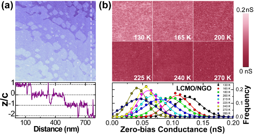
Topographs reveal flat terraces separated by growth steps multiple of the out-of-plane pseudocubic lattice parameter for both LCMO/NGO and LCMO/STO films Seiro08 ; Seiro07JMMM . In Fig. 1(a) we show a typical topograph for the 42 nm thick LCMO/NGO film. ZBC maps over an area covering a few topographic steps exhibit some dispersion of conductance values but no particular spatial pattern, as shown in Fig. 1(b) for LCMO/NGO and in Refs. Seiro07JMMM ; Seiro08Thesis for LCMO/STO. For both LCMO/NGO and LCMO/STO films the ZBC distribution is Gaussian at all temperatures, complementing our previous results at higher energies on LCMO/STO films Seiro07JMMM ; Seiro08 . Note that the ZBC level of a pixel in Fig 1(b) is not the average of ZBC values over the pixel suface, but the point value at the pixel center. If there were sub-pixel regions of very high and very low ZBC, as observed for Pr-doped LCMO films at 1.5-2 eV energies Ma05 , they should be manifest in the distribution of conductance values with a statistical weight proportional to their area fraction. The absence of a bimodal distribution of conductance values rather appears to indicate that there is no static phase separation in regions with strongly differentiated electronic properties. Assuming that a “different” phase has been missed by the discrete positioning of the tip, the surface fraction of it would be limited to roughly , casting a doubt on the role it plays in transport properties. The absence of regions with strongly differentiated tunneling spectroscopic properties (i.e. of a bimodal ZBC distribution) on LCMO films has also been reported for LCMO/NGO at Mitra05 and for cation ordered LCMO/MgO () at 115 K and 294 K Sudheendra07 .
For both strain states, not only the ZBC values but also the whole curves at any given temperature display no bimodal distribution over the field of view. As an example, Fig. 2(a) shows local LCMO/STO curves acquired over a 350 nm-long path at temperatures below and above the transition. The current vs. voltage curves in the metallic and insulating phases present a highly non-linear character and are remarkably alike. At first sight, one might be tempted to link these observations to insulating behavior (DOS). However, non-linear characteristics can appear also in metals (DOS), in particular if the DOS is non-constant in the vicinity of , or if the tunneling barrier is energy-dependent (e.g. for bias voltages that are a non-negligible fraction of the apparent workfunction barrier ). Further information on the DOS can be gained by a close inspection of the behavior of zero-bias conductance as a function of temperature.
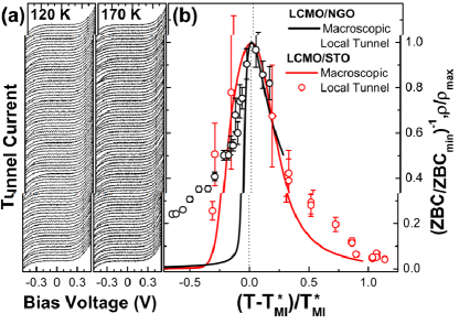
Figure 2(b) presents the temperature evolution of macroscopic resistivity and the inverse of the ZBC obtained from the spatially-averaged local curves, for both weakly and highly-strained films. We found that 1/ZBC is finite at all measured temperatures and roughly follows the behavior of macroscopic resistivity, increasing on warming in the low-temperature phase and decreasing on warming in the high-temperature phase. For a gapped DOS, a thermally-activated ZBC is expected, the activation energy yielding an estimate of the gap. In the high temperature phase, the activation energy obtained from the slope of our data vs. is comparable to the activation energy estimated from the slope of vs. , eV for LCMO/STO and eV for LCMO/NGO. However, the thermal activation here may be only apparent. The computational study in Ref. Yu08 proposes the occurrence of dynamic nanoscale AFM/CO correlations in the vicinity of the FM-AFM/CO phase boundary. If the characteristic lifetime of these correlations is shorter than the timescale of tunneling experiments, they will not be visualized in ZBC images. Nevertheless the presence of these correlations yields a finite DOS () at all temperatures for long Monte Carlo time scales in the calculation Yu08 , with a temperature dependence that follows the trend of macroscopic conductivity. This is indeed observed in our films, suggesting that the observed activated-like behavior does not come from a thermal excitation of carriers over a band gap but is due to dynamical CO/AFM correlations.
The DOS in Ref. Yu08 is not gapped above , but presents a pseudogap-like depletion in the vicinity of with a pseudogap energy scale that globally decreases on cooling. We can directly test these predictions by calculating the normalized or logarithmic conductance, , a method that attenuates the dependence on the tunneling barrier and yields a quantity proportional to the local DOS Feenstra94 . Normalized conductance (NC) curves are presented in Fig. 3 for both highly (left panel) and weakly (right panel) strained films. At high temperatures NC curves present a depletion around zero bias. This depletion survives down to low temperatures, but NC peaks (in the case of LCMO/STO) or kinks (for LCMO/NGO) become increasingly marked upon cooling. These features have been previously ascribed to the spectral signature of polarons Seiro08 ; Wei97 , the distance between the peaks being related to the polaron binding energy. In this context, a ‘polaron’ describes an object that is not just a charge coupled to a local lattice distortion, but which has a complex spin and orbital structure, rather like the AFM/CO correlations considered in Ref. Yu08 .
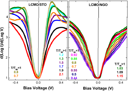
An important result of Fig. 3 is that there is neither a discontinuity nor an abrupt change in the shape of spectra across the insulator-to-metal transition. No hard gap opens on warming through but the DOS is depleted in the vicinity of at all measured temperatures. However, subtle and gradual changes in the spectral shape are observed as a function of temperature. In the insulating phase, on cooling towards the transition, ZBC decreases as peaks/kinks develop at the flanks of the depletion, indicating a spectral weight transfer from low to high energies. On further cooling, in the metallic phase spectral weight increasingly builds up at the chemical potential and the height of conductance peaks slightly decreases, see Fig. 3(a). In terms of the findings of Ref. Yu08 , these results can be interpreted as follows: In the insulating phase the AFM/CO correlation lifetime increases upon cooling, but decreases as ferromagnetic order sets in at . Although the short lifetime of the correlations hindered us to directly image them in conductance maps, they are manifest through the pseudogapped-like depletion of tunneling conductance and the temperature evolution of the ZBC. It is important to note that the calculations of Ref. Yu08 were performed in the clean limit. Quenched disorder is known to enhance the colossal magnetoresistance and extends the region of the phase diagram where it occurs Dagotto08 , but our results call for a systematic study of its effect on the AFM/CO correlations dynamics.
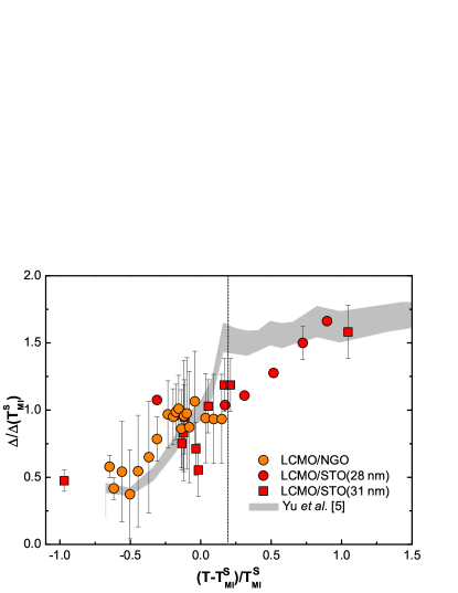
The width of the depletion or pseudogap, , was obtained for the curves in Fig. 3 as the half-distance between the two peaks (kinks) in the case of LCMO/STO(NGO) films. The pseudogap values are summarized in Fig. 4 for all samples Futinochi2 . The behavior of as a function of temperature is in qualitative agreement with the results of Ref. Yu08 , globally increasing on warming. In the vicinity of , the pseudogap energy changes its slope but further increases in the high-temperature phase.
In conclusion, we have carried out a detailed analysis of the tunnel spectra of manganite films that sheds light into the puzzling relation between the local electronic properties and macroscopic transport across the insulator-to-metal transition. Although both the insulating and metallic phases present a pseudogapped normalized conductance, spectral weight redistributes as a function of temperature in such a way that the temperature evolution of the macroscopic conductivity is tracked by the density of states at the chemical potential. A similar behavior was predicted in Ref. Yu08 , where nanoscale spin/charge correlations were found to be increasingly stable on cooling towards but their lifetime is reduced with the onset of ferromagnetic order. In addition, the predicted temperature evolution of the pseudogap energy Yu08 is consistent with the measured . This behavior is observed for highly and weakly strained films. Our results strongly support that dynamical spin/charge correlations play a preeminent role in the transport properties of colossal magnetoresistive manganites.
The authors thank Y. Rong for useful discussions and the Swiss National Science Foundation/MaNEP for financial support.
References
- (1) For a review, see for example: Y. Tokura, Colossal Magnetoresistive Oxides, Gordon and Breach Science Publishers, Amsterdam (2000), E. Dagotto, Nanoscale Phase Separation and Colossal Magnetoresistance, Springer-Verlag, Berlin (2003), T. Chatterji, Colossal Magnetoresistive Manganites, Kluwer Academic Publishers, Dordrecht/Boston/London (2004).
- (2) S. Seiro et al., Phys. Rev. B 77, 020407(R) (2008).
- (3) U. R. Singh et al, Phys. Rev. B 77, 014404 (2008).
- (4) H. M. Rønnow et al., Nature 440, 1025 (2006).
- (5) R. Yu et al., Phys. Rev. B 77, 214434 (2008).
- (6) S. Seiro, E. Koller, Y. Fasano, and Ø. Fischer, Appl. Phys. Lett. 91, 091913 (2007).
- (7) M. Bibes et al., Phys. Rev. B 66, 134416 (2002).
- (8) K.-H. Müller et al., J. Magn. Magn. Mater. 242-245, 447 (2002).
- (9) B. Vengalis et al., J. Magn. Magn. Mater. 211, 35 (2000).
- (10) J. H. Song, J.-H. Park, Y. H. Jeong, and T. Y. Koo, Physica B 312-313, 729 (2002).
- (11) M. Ziese, H. C. Semmelhack and K. H. Han, Phys. Rev. B 68, 134444 (2003).
- (12) S. Valencia, L. Balcells, B. Martínez, and J. Fontcuberta, J. Appl. Phys. 93, 8059 (2003).
- (13) L. Sudheendra et al., Phys. Rev. B 75, 172407 (2007).
- (14) S. Rößler et al., E. Phys. Lett. 83, 17009 (2008).
- (15) S. Seiro et al, J. Magn. Magn. Mater. 310, e243 (2007).
- (16) S. Seiro, PhD Thesis 3995, University of Geneva (2008).
- (17) J. X. Ma, D. T. Gillaspie, E. W. Plummer, J. Shen, Phys. Rev. Lett. 95, 237210 (2005).
- (18) J. Mitra et al, Phys. Rev. B 71, 094426 (2005).
- (19) In our experiments the apparent workfunction ranged between 1 and 1.5 eV.
- (20) R. M. Feenstra, Phys. Rev. B 50, 4561 (1994).
- (21) J. Y. T. Wei, N.-C. Yeh, R. P. Vasquez, Phys. Rev. Lett. 79, 5150 (1997).
- (22) E. Dagotto et al., J. Phys.: Condens. Matter 20, 434224 (2008).
- (23) The energy scale of the depletion in our films, comparable to the activation energy in resistivity, is well below the 1.5 eV observed by Fuchigami et al. in Phys. Rev. Lett. 102, 066104 for the reconstructed surface of a La5/8Ca3/8MnO3/Nb-STO film. This indicates that the surface of our films has not undergone this kind of reconstruction.