Magnetoresistive junctions based on epitaxial graphene and hexagonal boron nitride
Abstract
We propose monolayer epitaxial graphene and hexagonal boron nitride (-BN) as ultimate thickness covalent spacers for magnetoresistive junctions. Using a first-principles approach, we investigate the structural, magnetic and spin transport properties of such junctions based on structurally well defined interfaces with (111) fcc or (0001) hcp ferromagnetic transition metals. We find low resistance area products, strong exchange couplings across the interface, and magnetoresistance ratios exceeding 100% for certain chemical compositions. These properties can be fine tuned, making the proposed junctions attractive for nanoscale spintronics applications.
pacs:
72.25.-b, 73.43.Qt, 75.47.-m, 81.05.UwI INTRODUCTION
Graphene, a recently discovered two-dimensional form of carbon, has attracted unrivaled attention due to its unique physical properties and potential applications in electronics.Katsnelson (2007); Geim and Novoselov (2007) This nanomaterial is particularly promising for the field of spintronics, which exploits both the spin and the charge of electrons.Son et al. (2006); Tombros et al. (2007); Yazyev and Katsnelson (2008); Munoz-Rojas09 ; Yazyev and Katsnelson (2008); Yazyev09 ; Yazyev and Katsnelson (2008) One fundamental spintronic effect is the magnetoresistance, the change in electric resistance as a function of the relative orientation, either parallel or antiparallel, of the magnetization of two ferromagnetic layers separated by a nonmagnetic spacer layer.Heiliger et al. (2006a) Achieving high magnetoresistance ratios while keeping reasonably low electric resistance is crucial for many technological applications.Chappert et al. (2007) However, reaching this goal is currently hindered by material-specific restrictions such as the inability of producing well-ordered ferromagnet/spacer interfaces.Yuasa et al. (2004); Heiliger et al. (2006b)
Semimetallic graphene and its insulating counterpart, isostructural hexagonal boron nitride (-BN), are promising spacers as epitaxial monolayers of these materials can be grown by means of chemical vapor deposition (CVD) on a broad variety of metallic substrates.Oshima and Nagashima (1997); Berner et al. (2007); Coraux et al. (2008); Vázquez de Parga et al. (2008); Sutter et al. (2008); Martoccia et al. (2008) The quality of such epitaxial monolayers is very high and the covalent bonding network of both graphene and -BN is perfectly preserved upon the bonding to the substrate. Moreover, the growth of graphene and -BN on fcc(111) and hcp(0001) surfaces of ferromagnetic Co and Ni results in commensurate epitaxial layers due to the closely matching lattice constants.Oshima and Nagashima (1997) This has led to a theoretical prediction of perfect spin filtering and, thus, to extremely high magnetoresistance ratios in such junctions based on multilayer graphene (4 layers) and graphite.Karpan et al. (2007) However, the CVD growth on crystalline surfaces is self-inhibiting, that is only one epitaxial layer can be grown. The deposition of ferromagnetic nanoparticles on top of epitaxial -BN has also been demonstrated.Auwärter et al. (2002); Zhang et al. (2008) These interfaces further offer the opportunity of fine tuning their properties through the intercalation of other metals, such as Fe,Dedkov et al. (2008) CuDedkov et al. (2001) and Au.Varykhalov et al. (2008)
In this work, we suggest the use of monolayer graphene and -BN as covalently bonded spacer layers of minimal thickness in magnetoresistive junctions. Through first principles calculations we study the structural, magnetic and spin transport properties of such junctions based on first-row ferromagnetic transition metals: natural hcp and fcc Co, fcc Ni, as well as intercalated fcc Fe. We show that the proposed magnetoresistive junctions realize low electric resistances, strong interlayer exchange couplings, and magnetoresistance ratios exceeding 100% for certain chemical compositions.
This paper is organized as follows. In Sec. II we describe our computational methodology, including the first-principles approach to electronic transport. In Sec. III we report the atomic structure and electronic properties of the considered magnetoresistive junctions. Particular attention is devoted to the interlayer exchange couplings. The results of electronic transport calculations are discussed in Sec. IV. Section V concludes our work.
II COMPUTATIONAL METHODS
The electronic and atomic structure calculations were performed using the pwscf plane-wave pseudopotential code of the quantum-espresso distribution.Baroni et al. To achieve a good description of atomic structures, interlayer exchange couplings and spin transport properties, we chose the Perdew-Burke-Ernzerhof exchange-correlation density functional.Perdew et al. (1996) Ultrasoft pseudopotentials were used to describe core-valence interactions.Vanderbilt (1990) The valence wave functions and the electron density were described by plane-wave basis sets with kinetic energy cutoffs of 25 Ry and 250 Ry, respectively.Pasquarello (1992) The atomic structure of the magnetoresistive junctions considered in our work is illustrated in Fig. 1(a). Our investigation is restricted to only symmetric junctions, i.e. with the same metal on both sides of the spacer layer. Each ferromagnetic layer consisted of six atomic planes. The solutions for parallel and antiparallel relative spin orientations of these two layers were obtained by specifying appropriate initial orientations of the magnetic moments. The lateral unit cell of the studied interfaces is shown in Fig. 1(b). We considered bound configurations and determined the lowest-energy structures through the relaxation of atomic positions. For these configurations, we performed quantum transport calculations in the current perpendicular to plane configuration using the pwcond codeSmogunov et al. (2004) of the same package. The scattering region included the spacer monolayer and three adjacent monolayers of metal on both sides. We use the optimistic definition of the magnetoresistance ratio:
| (1) |
The spin-resolved quantum conductances for parallel ( for majority and minority spins, respectively) and antiparallel () configurations were calculated by integrating the corresponding -dependent transmission probabilities evaluated on a uniform grid of 6464 -points in the two-dimensional Brillouin zone.
III ATOMIC AND ELECTRONIC STRUCTURE
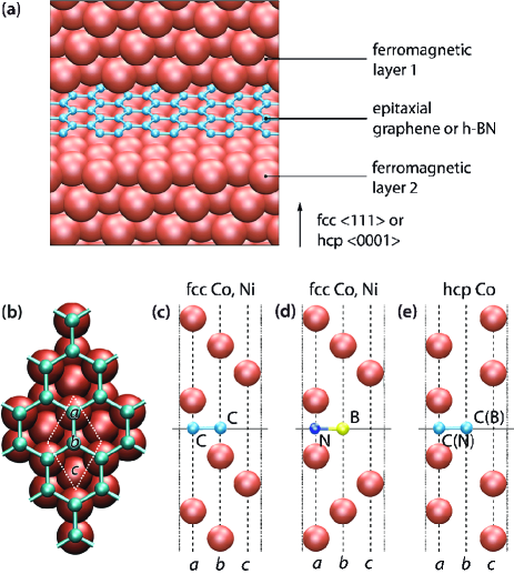
To determine the lowest energy structures of the junctions, we carried out structural relaxations for all possible stacking orders of the atomic planes in the vicinity of the spacer layer. The corresponding structures are shown in Fig. 1 for Co and Ni based junctions and summarized in Table 1 for all investigated chemical compositions. We find that both graphene (GR) and -BN bound to the transition metals (TM) display short metal-carbon and metal-nitrogen distances (2.19–2.45 Å) comparable to the sum of the corresponding covalent bond radii. The thickness of the spacer layer is thus comparable to that of a single atomic plane of the ferromagnetic metal. For the NiGRNi(fcc) junction we find a Ni–C distance of 2.19 Å, which is close to 2.18 Å calculated for the graphene chemisorbed on the Ni(111) surface (i.e. NiGR system). The latter value is in good agreement with the experimental value of 2.160.07 Å.Oshima and Nagashima (1997)
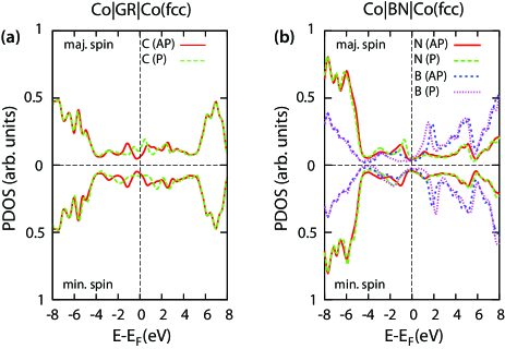
We now turn to the electronic structure of these magnetoresistive junctions. Figure 2 shows the spin-resolved projected density of states (PDOS) onto the light atoms (B, C and N) of the fcc Co junctions. One can see that the characteristic “Dirac cone” density of states of the free-standing graphene is not preserved upon the formation of the CoGRCo(fcc) interface [Fig. 2(a)]. This is consistent with the theoretically predictedKarpan et al. (2007) and experimentally observedGrüneis and Vyalikh (2008) strong hybridization between the electronic states of graphene and of the TM surface. Similarly, both B and N centered states fill the band gap of the insulating -BN [Fig. 2(b)]. In both cases, we very similarly find significant contributions of the epitaxial layer states to the density of states at the Fermi level. In the parallel (antiparallel) configuration of the graphene based junction, the induced magnetic moments on the carbon atoms in the unit cell are 0.005 (0.081 and 0.081). In the parallel configuration of the -BN junction, the induced magnetic moments of N and B atoms are 0.029 and 0.065, respectively. In the antiparallel configuration both vanish by symmetry.
| junction | stacking | MR | ||||
|---|---|---|---|---|---|---|
| order | (meV) | () | () | () | (%) | |
| FeGRFe(fcc) | 79 | 0.334 | 0.440 | 0.240 | 61 | |
| FeBNFe(fcc) | 63 | 0.256 | 0.297 | 0.111 | 149 | |
| CoGRCo(fcc) | 91 | 0.317 | 0.427 | 0.232 | 60 | |
| CoBNCo(fcc) | 46 | 0.263 | 0.268 | 0.210 | 26 | |
| NiGRNi(fcc) | 18 | 0.352 | 0.587 | 0.402 | 17 | |
| NiBNNi(fcc) | 3 | 0.207 | 0.722 | 0.299 | 55 | |
| CoGRCo(hcp) | 29 | 0.241 | 0.278 | 0.140 | 86 | |
| CoBNCo(hcp) | 44 | 0.222 | 0.241 | 0.140 | 66 |
The interlayer exchange coupling, the difference between the energies of parallel and antiparallel configurations, is a manifestation of the superexchange mechanism. It achieves rather high values [cf. Table 1] due to the ultimate thickness of the spacer layer. For Fe and Co, the antiparallel configuration is energetically favored. On the contrary, the parallel configuration is preferred for Ni. This intriguing crossover provides opportunity for fine tuning the interlayer exchange by varying the chemical composition of the ferromagnetic layers.
IV ELECTRONIC TRANSPORT
IV.1 Role of spacer material
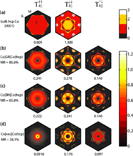
To understand the calculated quantum conductances and the resulting magnetoresistance ratios [cf. Table 1], we analyzed the -resolved transmission probabilities. First, we studied the effect of the spacer layer in hcp Co junctions which have the same lowest energy structure for both graphene and -BN [Fig. 3]. We found that both systems show strikingly similar -resolved transmission probability maps [compare Figs. 3(b) and 3(c)] and consequently quantum conductances. The and maps reveal major features of the projected hcp Co Fermi surfaces for the free-electron-like majority spin and mostly -symmetry minority spin electrons [Fig. 3(a)], which are relevant to the quantum conductances of bulk metals.Schep et al. (1998); Zwierzycki et al. (2008) The total transmission probabilities of the junctions in the parallel configurations constitute 40% and 20% of the Sharvin conductancesSharvin65 of bulk hcp Co along the (0001) direction. The quantum conductances in the antiparallel configuration are mostly determined by the overlap of and . Their values are consequently lower ( per unit cell for both spacer materials). The resulting magnetoresistance ratios are 86% and 66% for graphene and -BN junctions. Thus, in the regime of ultimate thickness the transport properties are largely independent of the electronic structure differences of the two spacer materials. The role of a single layer of covalent spacer material consists in fixing a certain stacking order at the interface and in providing a medium for the abrupt change of magnetization in the antiparallel configuration. Due to the metallic nature of the spacer layers [cf. Fig. 2] such junctions possess low resistance area products (310-15 m2) which makes them suitable for nanoscale spintronics applications such as the magnetic random access memories and spin transfer nano-oscillators. We classify the present systems as giant magnetoresistance (GMR) junctions. This contrasts to the spin transport through a vacuum gap of the same thickness which shows decaying with [Fig. 3(d)], a characteristic feature of tunneling.Belashchenko et al. (2004) The magnetoresistance ratio is about twice smaller (38%) in the case of tunneling through a vacuum gap. This allows us to conclude that in the limit of ultimate thickness the GMR effect is more efficient than the tunneling magnetoresistance.
IV.2 Role of ferromagnetic layers
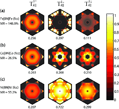
Next, we studied the dependence of transport properties on the ferromagnetic metal by considering fcc Fe, Co and Ni junctions in combination with -BN. For all three metals, the majority spin transmission in the parallel configuration, , undergoes little change along the Fe-Co-Ni series [Fig. 4]. This behavior stems from the similarity of the corresponding majority spin Fermi surfaces of the bulk metals, which are formed by partially filled bands. However, much larger differences are found for involving the minority electrons. These reflect the drastically different Fermi surfaces resulting from the interplay between and states. The increase of along the series can be attributed to the decrease of hybridization between and electrons upon the increase of band filling:Mazin (1999) in general, the free-electron-like states show higher transmission probabilities. The values are again determined by the overlap of and and tend to increase along the series. For the FeBNFe(fcc) junction we find a magnetoresistance ratio of 150%, the largest value among the compositions studied.
Further search of magnetoresistive junctions with improved characteristics may consist in exploring asymmetric junctions and the intercalation of some other chemical elements at the interfaces. We here demonstrate the second possibility. It has been suggested that the incorporation of submonolayer quantities of Cu at the TMGRn interface would reduce undesired hybridization between the states of graphene and of the metal surface at the price of substantially decreasing the magnetoresistance ratios.Karpan et al. (2007) However, we find that the decoupling of the spacer layer from the metal surface does not necessarily imply the loss of magnetoresistance. This can be achieved by intercalating the metals from the middle of the transition metals series, e.g. Mn, which show reduced binding to carbon systems.Pandey et al. (2001) Indeed, in the intercalated CoMn(1 ML)GRMn(1 ML)Co(hcp) junction the Mn–C distance increases to 2.95 Å and the interlayer exchange coupling decreases to 10 meV (to be compared with 29 meV for CoGRCo(hcp), cf. Table 1). Concurrently, the magnetoresistance ratio raises from 86% to 127%. The Mn layer is strongly spin polarized and antiferromagnetically coupled to hcp Co.
V CONCLUSIONS
In conclusion, we propose epitaxially grown monolayer graphene and -BN as ultimate thickness covalent spacers in transition metal based magnetoresistive junctions. Such junctions display well-ordered interfaces and can be produced through existing manufacturing processes. Their physical properties can be fine tuned in a broad range by varying the chemical composition. These systems show low resistance area products and typical GMR behavior with magnetoresistance ratios exceeding 100% for certain compositions. Both ferromagnetic and antiferromagnetic interlayer exchange couplings are found. These properties make the proposed junctions attractive for spintronics applications such as the magnetic random access memories and spin transfer nano-oscillators.
ACKNOWLEDGMENT
We acknowledge fruitful discussions with H. Brune, P. J. Kelly and S. Rusponi. We would like to thank A. Smogunov for his help with the pwcond code. The calculations were performed at the CSCS.
References
- Katsnelson (2007) M. I. Katsnelson, Materials Today 10, 20 (2007).
- Geim and Novoselov (2007) A. K. Geim and K. S. Novoselov, Nat. Mater. 6, 183 (2007).
- Tombros et al. (2007) N. Tombros, C. Jozsa, M. Popinciuc, H. T. Jonkman, and B. J. van Wees, Nature (London) 448, 571 (2007); N. Tombros, S. Tanabe, A. Veligura, C. Jozsa, M. Popinciuc, H. T. Jonkman, and B. J. van Wees, Phys. Rev. Lett. 101, 046601 (2008).
- Son et al. (2006) Y.-W. Son, M. L. Cohen, and S. G. Louie, Nature (London) 444, 347 (2006).
- Yazyev and Katsnelson (2008) O. V. Yazyev and M. I. Katsnelson, Phys. Rev. Lett. 100, 047209 (2008).
- (6) F. Muñoz-Rojas, J. Fernández-Rossier, and J. J. Palacios, Phys. Rev. Lett. 102, 136810 (2009).
- Yazyev and Katsnelson (2008) O. V. Yazyev and L. Helm, Phys. Rev. B 75, 125408 (2007); O. V. Yazyev, Phys. Rev. Lett. 101, 037203 (2008).
- (8) W. L. Wang, S. Meng, and E. Kaxiras, Nano Lett. 8, 241 (2008); O. V. Yazyev, W. L. Wang, S. Meng, and E. Kaxiras, Nano Lett. 8, 766 (2008); W. L. Wang, O. V. Yazyev, S. Meng, and E. Kaxiras, Phys. Rev. Lett. 102, 157201 (2009).
- Yazyev and Katsnelson (2008) O. V. Yazyev, Nano Lett. 8, 1011 (2008).
- Heiliger et al. (2006a) C. Heiliger, P. Zahn, and I. Mertig, Materials Today 9, 46 (2006a).
- Chappert et al. (2007) C. Chappert, A. Fert, and F. N. Van Dau, Nat. Mater. 6, 813 (2007).
- Yuasa et al. (2004) S. Yuasa, T. Nagahama, A. Fukushima, Y. Suzuki, and K. Ando, Nat. Mater. 3, 868 (2004).
- Heiliger et al. (2006b) C. Heiliger, P. Zahn, B. Y. Yavorsky, and I. Mertig, Phys. Rev. B 73, 214441 (2006b).
- Oshima and Nagashima (1997) C. Oshima and A. Nagashima, J. Phys.: Condens. Matter 9, 1 (1997).
- Berner et al. (2007) S. Berner, M. Corso, R. Widmer, O. Groening, R. Laskowski, P. Blaha, K. Schwarz, A. Goriachko, H. Over, S. Gsell, M. Schreck, H. Sachdev, T. Greber, and J. Osterwalder, Angew. Chem. Int. Ed. 46, 5115 (2007).
- Coraux et al. (2008) J. Coraux, A. T. N’Diaye, C. Busse, and T. Michely, Nano Lett. 8, 565 (2008).
- Vázquez de Parga et al. (2008) A. L. Vázquez de Parga, F. Calleja, B. Borca, J. M. C. G. Passeggi, J. J. Hinarejos, F. Guinea, and R. Miranda, Phys. Rev. Lett. 100, 056807 (2008).
- Sutter et al. (2008) P. W. Sutter, J.-I. Flege, and E. A. Sutter, Nat. Mater. 7, 406 (2008).
- Martoccia et al. (2008) D. Martoccia, P. R. Willmott, T. Brugger, M. Bjorck, S. Gunther, C. M. Schleputz, A. Cervellino, S. A. Pauli, B. D. Patterson, S. Marchini, J. Wintterlin, W. Moritz, and T. Greber, Phys. Rev. Lett. 101, 126102 (2008).
- Karpan et al. (2007) V. M. Karpan, G. Giovannetti, P. A. Khomyakov, M. Talanana, A. A. Starikov, M. Zwierzycki, J. van den Brink, G. Brocks, and P. J. Kelly, Phys. Rev. Lett. 99, 176602 (2007); V. M. Karpan, P. A. Khomyakov, A. A. Starikov, G. Giovannetti, M. Zwierzycki, M. Talanana, G. Brocks, J. van den Brink, and P. J. Kelly, Phys. Rev. B 78, 195419 (2008).
- Auwärter et al. (2002) W. Auwärter, M. Muntwiler, T. Greber, and J. Osterwalder, Surf. Sci. 511, 379 (2002).
- Zhang et al. (2008) J. Zhang V. Sessi, C. H. Michaelis, I. Brihuega, J. Honolka, K. Kern, R. Skomski, X. Chen, G. Rojas, and A. Enders, Phys. Rev. B 78, 165430 (2008).
- Dedkov et al. (2008) Yu. S. Dedkov, M. Fonin, U. Rudiger, and C. Laubschat, Appl. Phys. Lett. 93, 022509 (2008).
- Dedkov et al. (2001) Yu. S. Dedkov, A. M. Shikin, V. K. Adamchuk, S. L. Molodtsov, C. Laubschat, A. Bauer, and G. Kaindl, Phys. Rev. B 64, 035405 (2001).
- Varykhalov et al. (2008) A. Varykhalov, J. Sanchez-Barriga, A. M. Shikin, C. Biswas, E. Vescovo, A. Rybkin, D. Marchenko, and O. Rader, Phys. Rev. Lett. 101, 157601 (2008).
- (26) P. Giannozzi et al., http://www.quantum-espresso.org
- Perdew et al. (1996) J. P. Perdew, K. Burke, and M. Ernzerhof, Phys. Rev. Lett. 77, 3865 (1996).
- Vanderbilt (1990) D. Vanderbilt, Phys. Rev. B 41, R7892 (1990).
- Pasquarello (1992) A. Pasquarello, K. Laasonen, R. Car, C. Lee, and D. Vanderbilt, Phys. Rev. Lett. 69, 1982 (1992); K. Laasonen, A. Pasquarello, R. Car, C. Lee, and D. Vanderbilt, Phys. Rev. B 47, 10142 (1993).
- Smogunov et al. (2004) A. Smogunov, A. Dal Corso, and E. Tosatti, Phys. Rev. B 70, 045417 (2004); H. J. Choi and J. Ihm, Phys. Rev. B 59, 2267 (1999).
- Grüneis and Vyalikh (2008) A. Grüneis and D. V. Vyalikh, Phys. Rev. B 77, 193401 (2008).
- Schep et al. (1998) K. M. Schep, P. J. Kelly, and G. E. W. Bauer, Phys. Rev. B 57, 8907 (1998).
- Zwierzycki et al. (2008) M. Zwierzycki, P. A. Khomyakov, A. A. Starikov, K. Xia, M. Talanana, P. X. Xu, V. M. Karpan, I. Marushchenko, I. Turek, G. E. W. Bauer, G. Brocks, and P. J. Kelly, Phys. Status Solidi B 245, 623 (2008).
- (34) Yu. V. Sharvin, Zh. Eksp. Teor. Phys. 48, 984 (1965); Sov. Phys. JETP 21, 655 (1965).
- Belashchenko et al. (2004) K. D. Belashchenko, E. Y. Tsymbal, M. van Schilfgaarde, D. A. Stewart, I. I. Oleinik, and S. S. Jaswal, Phys. Rev. B 69, 174408 (2004).
- Mazin (1999) I. I. Mazin, Phys. Rev. Lett. 83, 1427 (1999).
- Pandey et al. (2001) R. Pandey, B. K. Rao, P. Jena, and M. A. Blanco, J. Am. Chem. Soc. 123, 3799 (2001).