Exciton polaritons in two-dimensional photonic crystals
Abstract
Experimental evidence of strong coupling between excitons confined in a quantum well and the photonic modes of a two-dimensional dielectric lattice is reported. Both resonant scattering and photoluminescence spectra at low temperature show the anticrossing of the polariton branches, fingerprint of strong coupling regime. The experiments are successfully interpreted in terms of a quantum theory of exciton-photon coupling in the investigated structure. These results show that the polariton dispersion can be tailored by properly varying the photonic crystal lattice parameter, which opens the possibility to obtain the generation of entangled photon pairs through polariton stimulated scattering.
pacs:
71.36.+c, 42.70.Qs, 78.55.Cr, 42.30.Kq, 71.35.-yThe strong coupling regime between light and matter is characterized by a reversible and coherent exchange of energy between a single material oscillator and a single mode of the electromagnetic field. A particular case is when excitons confined in a semiconductor Quantum Well (QW) are spectrally and spatially resonant with the mode of a vertical semiconductor microcavity, e.g. in structures similar to the Vertical Cavity Surface Emitting Laser VCSEL . If the coherent light-matter coupling overcomes excitonic and photonic dissipation rates, the strong coupling regime can be achieved in these structures Weisbuch ; Skolnick . As a result, exciton-photon hybrid quasiparticles named microcavity polaritons are formed.
Microcavity polaritons have bosonic statistics, fast interaction with the electromagnetic field, and strong optical nonlinearities related to their excitonic parts. These properties have been exploited to obtain a wealth of nonclassical phenomena in the solid state: coherent and macroscopically occupied matter-wave states Kasprzak ; Balili , optical spin Hall effect Leyder , and superfluidity Amo among others. Their strong optical nonlinearities have been used to demonstrate low-power parametric oscillations of matter-waves Savvidis ; Stevenson ; Tignon ; Saba : considerable interest has been devoted to polariton parametric scattering with the goal of realizing a semiconductor-based, monolithic and micron-sized source of entangled photon pairs. However, quantum correlation experiments are usually hindered by the great intensity difference between signal and idler beams, which is intrinsic to the dispersion of polariton branches in planar microcavities Karr : possible solutions have been sought by modifying the microcavity geometry Tignon ; Pillars .
Photonic crystals can be used to tune the photonic mode dispersion by suitably modifying the sample design Joannopoulos . Photonic crystals in the strong coupling regime give the unique possibility to engineer the dispersion of polariton branches. New ways to achieve phase matching for parametric scattering, e.g. to obtain signal and idler beams of comparable intensity, can thus be envisioned, opening the possibility of measuring quantum correlations between signal and idler polaritons. Early experimental evidence of polaritons in photonic crystals has been reported by using polymers sputtered on gratings Ishihara ; shimada02 . Polymers undergoing strong coupling have very strong oscillator strengths but do not show optical nonlinearities. Although theoretically proposed Gerace , polaritons in photonic crystals have never been reported in semiconductors, where nonlinearities are very high Saba . The main problem is that, in many semiconductor systems, and in particular in GaAs-based samples, patterning the QW results in a severe reduction of the exciton lifetime by nonradiative recombination at hole sidewalls Vuckovic , and consequently in the loss of strong coupling Koch .
Here we report the first experimental evidence of strong coupling between excitons confined in a semiconductor QW and the photonic modes of a two-dimensional photonic crystal. To avoid issues related to nonradiative recombination, we adopt an original design: the photonic lattice is spatially separated from the QWs so that polaritons only experience the periodic potential through their photonic part, while leaving the QW intact.
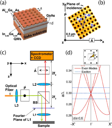
The sample, schematically shown in Fig. 1a, was grown by molecular beam epitaxy on a GaAs substrate. A 140 nm thick Al0.8Ga0.2As cladding was first deposited, followed by a 148 nm thick GaAs core with three 8 nm thick In0.05Ga0.95As QWs at its center, a second 140 nm thick Al0.8Ga0.2As cladding and finally a 100 nm GaAs top layer. The top layer was patterned by inductively coupled plasma etching Sagnes with a square lattice of circular air holes (see Fig. 1b): areas with different lattice parameters =245, 250, 255, and 260 nm were defined. The nominal etch depth is 120 nm. The periodic corrugation yields a dispersion-folding on the guided modes of the slab waveguide within the first Brillouin zone (Fig. 1d, upper panel), making them radiative around normal incidence (-point). Such folding depends on the lattice parameter, : for different lattice parameters, the resonance condition between the QW exciton and the photonic modes changes within the dispersion diagram. This is the essence of the polariton dispersion engineering discussed in the following, and it is shown in the calculated mode dispersion in Fig. 1d.
The sample was kept at low temperature in a He-cooled cold finger cryostat. The experimental set-up is outlined in Fig. 1c. To probe the elementary excitations of the system two different techniques were used: photoluminescence (PL) and resonant scattering (RS) of white light. This latter approach relies on sending a linearly polarized white light beam along the -axis (by the polarizer in Fig. 1c) and analyzing the reflected light in crossed polarization through a second polarizer along (). The photonic modes of the sample have a symmetry that can be even (i.e. having the electric field mainly polarized in the QW plane, TE-like) or odd (i.e. with the electric field mainly polarized perpendicular to the QW plane, TM-like). A crucial point in the present experiment is that the plane of incidence is tilted by with respect to the X lattice direction (Figs. 1b,c) and is not a mirror plane of the structure. While most of the reflected light keeps the polarization specified by the polarizer , when the incoming beam is resonant with a photonic/polaritonic mode a small amount of light is coupled to the opposite polarization, i.e. parallel to . Thus, the scattering signal is resonantly enhanced Williams and the modes appear as peaks over an almost vanishing background. The RS signal is a measure of the extinction of light due to its coupling with the sample and can be used to probe the dispersion of the modes in a wide spectral range: in this sense, it is analogous to the resonant Brillouin scattering technique for measuring the dispersion of exciton-polaritons in bulk semiconductors Ulbrich . PL spectra are obtained on the same set-up employing a laser pump at 1550 meV. Both the laser pump and the white light beam are focused on a 20 m-diameter spot on the sample surface by a microscope objective (L1 in Fig. 1a), that is also used to collect the emitted/reflected light. The plane of incidence is determined by the entrance slit of the spectrophotometer (parallel to in the frame of Fig. 1) and resolution in the angle of incidence () is obtained by directly imaging the Fourier plane of L1 onto the slit.

Polariton states, i.e. mixed radiation-matter quasiparticles, are expected to occur when the dimensionality of photon states is equal to (or, possibly, smaller than) that of the exciton Andreani-Varenna . Given the energies and of the uncoupled exciton and photonic modes and the respective dissipation rates and , the energies of the polariton eigenstates are simply described by Skolnick :
| (1) | ||||
where is the coupling constant between excitons and photons (half of the vacuum Rabi splitting). Equation 1 implies that polaritons anticross in reciprocal space, where the uncoupled modes would cross instead: the observation of such anticrossing is a clear signature of the strong coupling regime.
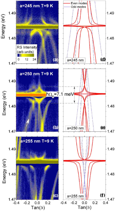
Low temperature RS measurements as a function of the incidence angle, , are shown in Figs. 2a,b,c for samples with =245, 250, and 255 nm, respectively. All spectra display an anticrossing between the dispersive modes and the exciton line at 1.485 eV, proving the occurrence of a strong coupling regime. Both the upper and lower polariton branches are clearly visible on either side of the exciton and the polariton linewidth remains well below 1 meV in all spectra; the measured Rabi splitting is meV, comparable to what has been reported for planar microcavities. Notice that, without coupling with the exciton, the modal dispersion would be linear, as discussed below. Figure 2 highlights that the original shape of polariton dispersions in such photonic crystals : for instance the diamond-like shape of the modes in Fig. 2b is completely different from the S-shaped dispersion of microcavity polaritons Skolnick . Moreover the polariton dispersion dramatically dependends on the lattice constant: changing by only 2% (5 nm) substantially reshapes the branches.
We model the system under investigation by calculating the photonic modes for the planar waveguide in the two-dimensional lattice as in Fig. 1d. Exciton-photon coupling is described by a full quantum formulation, as detailed in Ref. Gerace : the Rabi splitting in the polariton mode dispersion depends on the overlap between the guided modes of the slab waveguide and the QW exciton envelope function, as well as on the oscillator strength per unit area nota . The resulting polariton dispersions are reported in Figs. 2d,e,f, for the same lattice parameters as in Figs. 2a,b,c. Overall, the details of the polariton modes are complicated by the tilted plane of incidence () with respect to the X direction, which removes photonic mode degeneracies. Two photonic branches for each parity can be distinguished at the -point (), but only even modes strongly couple to the excitons. There is a good agreement between theory and experiment: the calculated Rabi splitting for these structures is meV and compares very well with the experimentally determined value of meV , as it can be easily seen by directly comparing Figs. 2b and e. Notice the presence of additional polariton branches in the measurements, which are not reproduced by the theory (an instance is highlighted by a white arrow in Fig. 2b). These additional modes appear only when the plane of incidence does not correspond to a high symmetry direction of the lattice (M or X) and may be related to finite lateral size of the samples: further theoretical and experimental investigation is underway to confirm this interpretation.
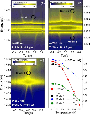
Measured PL spectra are shown in Figs. 3a,b and c. At such low temperatures, only polariton states lying a few meV from the exciton are enough populated to efficiently contribute to the PL signal, and the energy scale is consequently expanded in the figure. Polariton dispersion lines in emission are exactly equivalent to those reported in RS, confirming the occurrence of strong coupling in these samples. The exciton line at 1.485 eV is much more intense than the polariton lines. This is mainly due to two reasons: first, in the present experiment we collect the PL signal on a much wider region than the excitation spot, so that we measure also the signal coming from diffused excitons outside the patterned region. Second, only exciton states with symmetry close to the photonic mode are strongly coupled, while the majority of states remain in weak coupling with the electromagnetic field Gerace .
To evidence the difference between strong and weak coupling in our samples, PL measurements with increasing temperature () are plotted in Figs. 4a,b c for a sample with =260 nm. At T=70 K the sample is still in strong coupling, and shows the same anticrossing as at T=8 K (Figs. 4a,b). Above 80 K the Rabi splitting is progressively reduced and at T=250 K (Fig. 4c) strong coupling is lost and the photonic modes cross the exciton resonance. As an illustration, fig. 4d shows the energy variation with temperature of the exciton and of three modes chosen around the exciton at (modes 1 and 2, see black circles in Figs. 4a,b) and at low energy at (mode 3 see black circle in Fig. 4c) extracted from the spectra. Since the exciton redshift is stronger than that of the photonic modes, increasing temperature changes the detuning between exciton and modes. The exciton and mode 3 cross above 200 K, which evidences they are in weak coupling. On the other hand, modes 1 and 2 anticross at 45 K, and are thus in strong coupling. Their energies can be fitted by using Eq. 1, in which the uncoupled photonic mode, , is assumed to have the same dependence on the temperature as mode 3. This loss of strong coupling at high temperature can be understood considering the exciton dephasing rate in Eq. 1: increasing temperature means increasing until the term under square root becomes negative, i.e. excitons dephase in a time before a single Rabi oscillation can be completed.
In conclusion, we have shown the strong coupling regime of quantum-well excitons in two-dimensional photonic crystals through both resonant scattering and photoluminescence experiments at low temperature. The present results will open new directions for polariton research: the possibility of engineering phase matching is a considerable step towards achieving a compact and integrable solid-state source of entangled photon pairs. Further applications can be envisioned for polaritons in large band gap materials. Although the strong coupling regime has been already reported at room temperature in GaN Semond ; Grandjean , ZnO Morkoc and CuCl Nakayama , fabrication of high quality microcavities for these materials is often impractical due to the large number of required layers. Using planar photonic crystals, and in particular the present design that leaves the active region intact, will turn to be effective for obtaining strong coupling with high quality optical modes at room temperature.
The authors acknowledge M. Malvezzi for fruitful discussions and F. Manni for participation in the early part of the work. This work was supported by CNISM through the ”Innesco” initiative. Financial support from Fondazione Cariplo through project 2007-5259 is acknowledged.
References
- (1) K. Iga, IEEE J. Sel. Topics in Quantum Electron. 6, 1201 (2000).
- (2) C. Weisbuch, M. Nishioka, A. Ishikawa, and Y. Arakawa, Phys. Rev. Lett. 69, 3314 (1992).
- (3) M.S. Skolnick, T.A. Fisher, and D.M. Whittaker, Semicond. Sci. Technol. 13, 645 (1998).
- (4) J. Kasprzak et al., Nature 443, 409 (2006).
- (5) R. Balili et al., Science 316, 1007 (2007).
- (6) C. Leyder et al., Nature Physics 3, 628 (2007).
- (7) A. Amo, et al., Nature 457, 291 (2009); A. Amo et al., arXiv:0812.2748 (2008).
- (8) P.G. Savvidis et al., Phys. Rev. Lett. 84, 1547 (2000).
- (9) R.M. Stevenson et al., Phys. Rev. Lett. 85, 3680 (2000).
- (10) C. Diederichs et al., Nature 440, 904 (2006).
- (11) M. Saba et al., Nature 414, 731 (2001).
- (12) J.P. Karr, A. Baas, and E. Giacobino, Phys. Rev. A 69, 063807 (2004).
- (13) D. Bajoni et al., Appl. Phys. Lett. 90, 051107 (2007).
- (14) L.C. Andreani, in Electron and Photon Confinement in Semiconductor Nanostructures, edited by Deveaud, B., Quattropani, A., and Schwendimann, P. (IOS Press, Amsterdam, 2003), p. 105.
- (15) J.D. Joannopoulos, S.G. Johnson, J.N. Winn, and R.D. Meade, Photonic Crystals: Molding the Flow of Light. (Princeton University Press, Princeton, 2008).
- (16) T. Fujita, Y. Sato, T. Kuitani, and T. Ishihara, Phys. Rev. B 57, 12428 (1998).
- (17) R. Shimada, A.L. Yablonskii, S.G. Tikhodeev, and T. Ishihara, IEEE J. Quant. Electron. 38, 872 (2002).
- (18) D. Gerace, and L.C. Andreani, Phys. Rev. B 75, 235325 (2007).
- (19) D. Englund, H. Altug, and J. Vučković, Appl. Phys. Lett. 91, 071124 (2007).
- (20) T. Stroucken, R. Eichmann, L. Banyai, and S.W. Koch, J. Opt. Soc. Am. B 19, 2292 (2002).
- (21) R. Braive et al., Opt. Lett. 34, 554 (2009).
- (22) M. McCutcheon et al., Appl. Phys. Lett. 87, 221110 (2005).
- (23) R. Ulbrich, and C. Weisbuch, Phys. Rev. Lett. 38, 865 (1977).
- (24) We take cm-2, as appropriate for the heavy-hole exciton of a single, 8 nm-thick InGaAs QW [R.C. Iotti, L.C. Andreani, Phys. Rev. B 56, 3922 (1997)], and multiply it by to simulate the fabricated structure with 3 QWs in the GaAs core. The exciton linewidth is assumed to be meV, from experimental characterization. No other adjustable parameter was used in the theoretical analysis.
- (25) F. Semond et al., Appl. Phys. Lett. 87, 021102 (2005).
- (26) R. Butté et al., Phys. Rev. B 73, 033315 (2006).
- (27) R. Shimada et al., Appl. Phys. Lett. 92, 011127 (2008).
- (28) G. Oohata et al., Phys. Rev. B 78, 233304 (2008).