Spin polarization control by electric means: proposal for a spin diode
Abstract
A scheme of spin diode is proposed that uses a step-like quantum wire with Rashba spin-orbit interaction, connected to two leads with different width. It is shown that a very large vertical spin-polarized current can be generated when electrons transmit from the narrow lead to the wide lead, however, it vanishes or becomes very weak when the transport direction is reversed. This difference is revealed to arise from the different local density of electron states of the quantum wire, which is dependent on the direction of bias. The spin-polarized current in the proposed structure can be generated and manipulated by purely electric means and with strong a robustness against disorder, displaying the feasibility of this structure for a real application.
pacs:
73.21.Hb, 71.70.Ej, 72.25.DcSpin-dependent electron transport has attracted intense attention because of its potential application to spintronics,1,2 in which electron spin instead of charge degree of freedom is employed to store and communicate information. One key requirement in the development of spintronics is to be capable of generating and manipulating excess spin in nonmagnetic semiconductor by all electrical means. The Rashba spin-orbit interaction (SOI)3-5 due to the structure inversion asymmetry in heterostructures may provide a way to satisfy this goal, since its strength can be controlled by an additional gate voltage.6-7
Various spintronic devices have been put forward based on the effects of Rashba SOI. A spin field effect transistor has been suggested by Datta and Das,8 demonstrating that the electron spin rotation can be modulated by the Rashba SOI. Spin transistors which can be used as spin valves through the transmission gaps induced by the periodically SOI-modulated structure,9-10 or the control of spin lifetime in an InAs lateral transport channel11 have been studied previously. In addition, spin filters based on SOI in T-shape electron waveguide,12-16 quantum wire,17-22 wire networks,23 and quantum nanoring24 have been proposed. Recently, Zhai et al have investigated the spin transport properties of a two-terminal hornlike waveguide with Rashba SOI and found that a quite different magnitude of spin conductance can be achieved when the transport direction is reversed, which can be utilized to devise a spin current diode.25 However, only transversal spin conductance could be nonvanishing in the proposed structure because of its mirror symmetry with respect to the longitudinal axis. Further, the robustness of the spin conductance against disorder, which is essential for a real application, remains unclear. In our previous work,26 we show that a nonzero vertical spin-polarized current can also be obtained once the mirror symmetry with respect to the longitudinal direction is broken and it can survive even in the presence of strong disorder. Inspired by the above two works, we will show, in this brief report, that the spin transport properties of a Rashba step-like quantum wire can be used to design an ideal spin diode device, tolerating to a strong disorder.
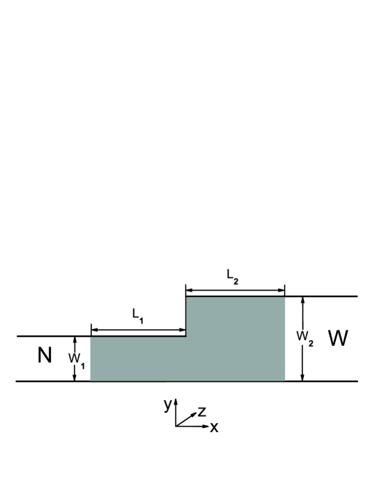
The system studied in present work is schematically depicted in Fig. 1, where a two-dimensional electron gas (2DEG) in the plane is restricted to a step-like quantum wire by a hard-wall transverse confining potential . The 2DEG is confined in a asymmetric quantum well, where the SOI is assumed to arise dominantly from the Rashba mechanism. The quantum wire consists of two regions. The narrow (wide) region has a length () and a uniform width (), connected to the narrow (wide) lead with the same width. The two connecting leads are normal-conductor electrodes without SOI since we are only interested in spin-unpolarized injection. Such kind of system can be described by discrete lattice model. The tight-binding Hamiltonian including the Rashba SOI on a square lattice is given as follow,
| (1) |
where
| (2) |
and
| (3) |
in which is the creation (annihilation) operator of electron at site with spin , is Pauli matrix, and is the on-site energy with the hopping energy , where and are the effective mass of electron and lattice constant, respectively. The SOI strength is with the Rashba constant . The Anderson disorder can be intrduced by the fluctuation of the on-site energies, which distributes randomly within the range width [ with ].
In the ballistic transport, the two-terminal spin-resolved conductance is obtained from the Landauer-Bttiker formula27
| (4) |
where with the self-energy from the narrow (wide) lead , the trace is over the spatial degrees of freedom, and is the retarded (advanced) Green function of the whole system, which can be computed by the well-known recursive Green function method.28,29
The local density of electron states (LDOS) is described as30
| (5) |
where is the spectral function, and is the electron energy. In the following calculation, the structural parameters of the wire are fixed at , , and . All the energy is normalized by the hoping energy . And the axis is chosen as the spin-quantized axis so that represents the spin-up state and denotes the spin-down state. The total charge conductance and the vertical spin polarization are defined as and , respectively.
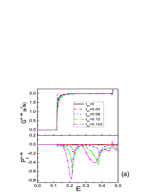
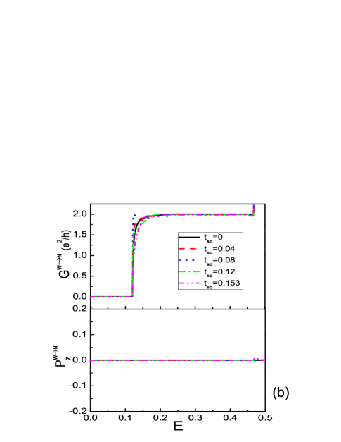
Figure 2(a) shows the total charge conductance and the vertical spin polarization as function of the electron energy for various Rashba SOI strengths when electrons travel the considered structure from the narrow lead to the wide lead (the forward biased case). A step-like structure appears in the charge conductance as the electron energy because the lowest one pair of subbands of the narrow region become propagating modes.26 Apart from the step-like structure, an oscillation also emerges in the conductance when the Rashba SOI is applied to the wire, which results from the interference between the forward and backward electron waves caused by the SOI-induced potential well. The oscillation periodicity is related to the wave vectors of the propagating modes so that the oscillation becomes apparent just above the threshold of the lowest pair of subbands where the wave vectors turn out to be smaller.31 Interestingly, a vertical spin-polarized current is generated when the outgoing lead supports two or more pairs of propagating modes, namely, . In particular, a very large spin polarization can be achieved around the thresholds of the third and fourth pairs of propagating modes of the wide region, i.e, and , respectively. Moreover, the magnitude of the spin polarization can be tuned by the Rashba SOI strength, namely, the additional gate voltage. Figure 2(b) plots the total charge conductance and the vertical spin polarization as function of the electron energy for various Rashba strengths when electrons travel the considered structure from the wide lead to the narrow lead (the backward biased case). It is worth to note that the total charge conductance is the same as that in Fig. 2(a) because of the time-reversal symmetry. However, the spin polarization in this case is zero as because there are only one pair of propagating modes in the outgoing lead32 or very small when .
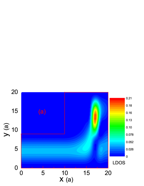
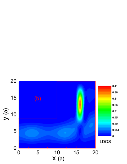
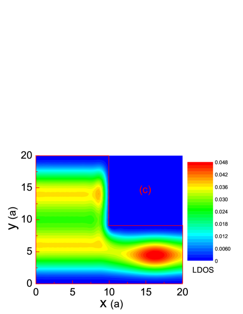
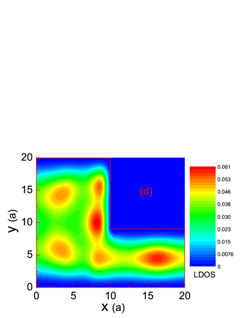
The remarkable difference in the spin polarization between the forward and backward transport directions can be utilized to devise a spin diode. The physical mechanism of this device is attributed to the structure-induced bound state in the quantum wire. The LDOS of the quantum wire in both the forward and backward biased cases is shown in Fig. 3. The electron energy is taken to be . The strength of Rashba SOI in Figs. 3(a) and 3(c), while it is set at in Figs. 3(b) and 3(d). As shown in Fig. 3(a), for the quantum wire in the forward biased case and without Rashba SOI, a regular stripe appears in the narrow region that represents one pair of propagating modes, whereas an obvious bound state is found to exist in the top of the wide region. The formation of the bound state origins from the fact that electrons are equivalent to be injected from the potential barrier area (the narrow region) to the potential well area (the wide region). As a consequence, higher-index propagating modes are preferred to be populated inside the wide region.33 The bound state in the wide region becomes more obvious when the Rashba SOI is added to the quantum wire due to the SOI-induced potential well, as seen in Fig. 3(b). This bound state couples to the continuous one through Rashba intermixing resulting in the large vertical spin-polarized current. Similarly, the LDOS of the quantum wire in the backward biased case is shown in Figs. 3(c) (without SOI) and 3(d) (with SOI). There are two regular stripes in the wide region and a regular stripe in the narrow region. It is important to mention that no obvious bound state formed in the wire in this case. Therefore, the spin polarization is very small even there are more than one pair of propagating modes in the narrow lead () or vanishes when there are only one pair of propagating modes () in the narrow lead.
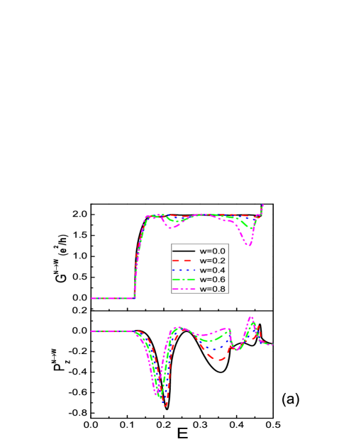
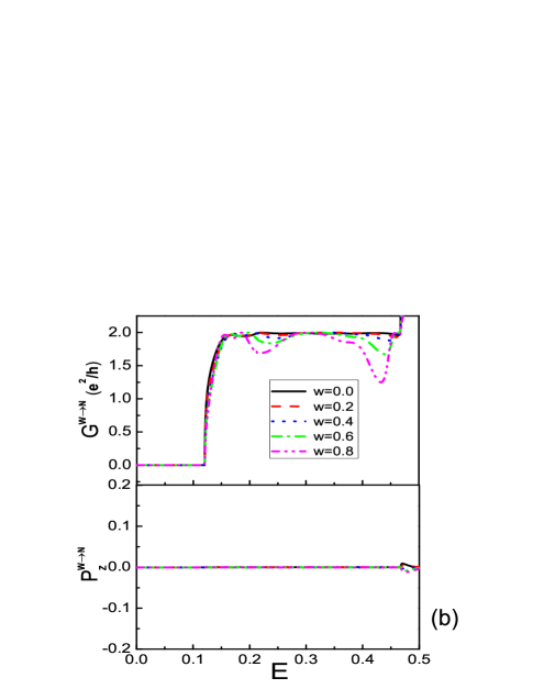
The above proposed spin diode is based upon a perfectly clean system, where no elastic or elastic scattering happens. Now we show the feasibility of this device for a real application by analyzing the robustness of the spin-polarized current against the Anderson disorder. The total charge conductance and the vertical spin polarization as function of the electron energy for (weak and strong) different disorders are illustrated in Fig. 4. The Rashba strength is set at . By comparing with the magenta (dash dot dot) line in Fig. 2, the step-like charge conductance is destroyed with the increasing of the disorder strength. However, the spin polarization around the thresholds of the third pairs of propagating modes of the wide region still larger than as [see the lower panel in Fig. 4(a)], which indicates that the spin-polarized current can still survive even in the presence of strong disorder when electrons transport in the forward direction. More surprisingly, the spin polarization almost has nothing to do with the disorder when electrons transport in the backward direction, as shown in the lower panel in Fig. 4(b).
In conclusion, a scheme for a spin diode is proposed by investigating a Rashba step-like quantum wire connected two leads with different width. A very large vertical spin polarized current can be obtained when the forward bias is applied to the structure, while it is suppressed strongly when the direction of bias is reversed, owing to the different LDOS of the wire. The spin-polarized current can be rectified by purely electric method and it is robust against disorder. Thus the proposed structure does not require the application of magnetic fields, external radiation or ferromagnetic leads, and has great potential for real applications.
This work was supported by the National Natural Science Foundation of China under Grant No. 10774112.
References
- (1) 1D. D. Awschalom, D. Loss, and N. Samarth, Semiconductor Spintronics and Quantum Computation (Springer, Berlin, 2002)
- (2) 2I. Zutic, J. Fabian, and S. Das Sarma, Rev. Mod. Phys. 76, 323 (2004).
- (3) 3E. I. Rashba, Sov. Phys. Solid State 2, 1109 (1960).
- (4) 4Y. A. Bychkov and E. I. Rashba, J. Phys. C 17, 6039 (1984).
- (5) 5G. Dresselhaus, Phys. Rev. 100, 580 (1955).
- (6) 6J. Nitta, T. Akazaki, H. Takayanagi, and T. Enoki, Phys. Rev. Lett. 78, 1335 (1997).
- (7) 7G. Engels, J. Lange, Th. Schpers, and H. Lth, Phys. Rev. B 55, R1958 (1997).
- (8) 8S. Datta and S. Das, Appl. Phys. Lett. 56, 665 (1990).
- (9) 9X. F. Wang, P. Vasilopoulos, and F. M. Peeters, Phys. Rev. B 65 165217 (2002).
- (10) 10X. F. Wang and P. Vasilopoulos, Phys. Rev. B 68 035305 (2003).
- (11) 11K. C. Hall, W. H. Lau, K. Gndodu, M. E. Flatt and T. F. Boggess, Appl. Phys. Lett. 83, 2937 (2003).
- (12) 12A. A. Kiselev and K. W. Kim, J. Appl. Phys. 94, 4001 (2003).
- (13) 13M. Yamamoto, T. Ohtsuki, and B. Kramer, Phys. Rev. B 72 115321 (2005).
- (14) 14F. Zhai and H. Q. Xu, Phys. Rev. B 76 035306 (2007).
- (15) 15S. Bellucci and P. Onorato, Phys. Rev. B 77 075303 (2008).
- (16) 16M. Yamamoto and B. Kramer, J. Appl. Phys. 103, 123703 (2008).
- (17) 17J. Ohe, M. Yamamoto, T Ohtsuki, and J. Nitta, Phys. Rev. B 72, 041308(R) (2005).
- (18) 18Q. F. Sun and X. C. Xie, Phys. Rev. B 71 155321 (2005).
- (19) 19M. Lee and C. Bruder, Phys. Rev. B 73, 085315 (2006).
- (20) 20L. G. Wang and K. Chang, J. Appl. Phys. 99, 043701 (2006).
- (21) 21Z. Y. Zhang, J. Phys: Condens. Matter 19 016209 (2006).
- (22) 22G. H. Liu and G. H. Zhou, J. Appl. Phys. 101, 063704 (2007).
- (23) 23H. X. Wang, S. J. Xiong, and S. N. Evangelou, Phys. Lett. A 356 376 (2006).
- (24) 24P. Fldi, O. Klmn, M. G. Benedict, and F. M. Peeters, Phys. Rev. B 73 155325 (2006); P. Fldi, O. Klmn, M. G. Benedict, and F. M. Peeters, Nano Lett. 8 2556 (2008). 25F. Zhai, K. Chang, and H. Q. Xu, Appl. Phys. Lett. 92 102111 (2008).
- (25) 26X. B. Xiao, X. M. Li, and Y. G. Chen, e-print arXiv:cond-mat/0906.3561 (unpublished).
- (26) 27M. Bttiker, Phys. Rev. Lett. 57 1761 (1986).
- (27) 28P. A. Lee and D. S. Fisher, Phys. Rev. Lett. 47 882 (1981).
- (28) 29T. Ando, Phys. Rev. B 44 8017 (1991); M. J. clennan,Y. Lee, and S. Datta, Phys. Rev. B 43 13846 (1991); H. U. Baranger, D. P. Divincenzo, R. A. Jalaber, and A. D. Stone, Phys. Rev. B 44 10637 (1991).
- (29) 30S. Datta, Electronic Transport in Mesoscopic Systems (Cambridge University Press, New York, 1997).
- (30) 31J. Wang, H. B. Sun, D. Y. Xing, Phys. Rev. B 69 085304 (2004).
- (31) 32F. Zhai and H. Q. Xu, Phys. Rev. Lett. 94, 246601 (2005).
- (32) 33F. Zhai and H. Q. Xu, Phys. Rev. B 76 035306 (2007).
- (33)