Strain and Electric Field Modulation of the Electronic Structure of Bilayer Graphene
Abstract
We study how the electronic structure of the bilayer graphene (BLG) is changed by electric field and strain from ab initio density-functional calculations using the LMTO and the LAPW methods. Both hexagonal and Bernal stacked structures are considered. The BLG is a zero-gap semiconductor like the isolated layer of graphene. We find that while strain alone does not produce a gap in the BLG, an electric field does so in the Bernal structure but not in the hexagonal structure. The topology of the bands leads to Dirac circles with linear dispersion in the case of the hexagonally stacked BLG due to the interpenetration of the Dirac cones, while for the Bernal stacking, the dispersion is quadratic. The size of the Dirac circle increases with the applied electric field, leading to an interesting way of controlling the Fermi surface. The external electric field is screened due to polarization charges between the layers, leading to a reduced size of the band gap and the Dirac circle. The screening is substantial in both cases and diverges for the Bernal structure for small fields as has been noted by earlier authors. As a biproduct of this work, we present the tight-binding parameters for the free-standing single layer graphene as obtained by fitting to the density-functional bands, both with and without the slope constraint for the Dirac cone.
pacs:
81.05.Uw; 73.22.-fI Introduction
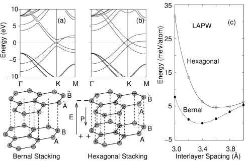
Recently bilayer graphene (BLG) has been shown to possess a band gap in the presence of an external electric field,ohta ; oostinga an effect that has important implications for transport across the graphene layers and for possible device applications. While the freestanding BLG is a zero band gap semiconductorlatil ; mccann1 like the single layer graphene (SLG), an applied electric field through an external gate induces an asymmetric potential between the graphene layers, which in turn opens a gap between the valence and the conduction bands in the Bernal structure.mccann1 ; mccann2 ; castro ; min ; nilsson It has been recently notedliu that graphene exhibits the hexagonal stacking surprisingly often, surprising because of the higher energy of the hexagonal structure. In the hexagonal structure, the two graphene layers are stacked vertically on top of one another, while in the Bernal strcuture, one layer is rotated with respect to the other as indicated in Fig. 1, so that half of the atoms are directly above the carbon atoms in the first layer, while the remaining half lie on top of the hexagon centers. The difference in symmetry between the Bernal and the hexagonal structures leads to substantial differences in the band structure, especially, in the formation of a band gap, an effect we study in this paper.
To tune the field-induced band gap of the BLGs for practical applications in nano-electronic devices, it is important to examine the factors having strong influence on its electronic structure. Electronic structure of BLG was shown to be sensitive to the interlayer spacing due to coupling between the graphene layersohta1 ; varchon . Hence, a uniaxial strain, which changes the interlayer spacing, could modulate the field induced band gapguo ; raza . The other factor that controls the gap is the screening of the electric field. An applied electric field causes unequal charge distribution among the graphene layers which in turn creates a polarized electric field in the opposite direction,min thereby reducing the effective electric field. A detail investigation through density-functional calculations is required to understand the effect of the electric field and strain on the electronic structure.
While the electronic structure of the Bernal BLG has been theoretically examined, such studies have not been performed for the hexagonal structure to our knowledge. In this paper, we report results from density-functional calculations and tight-binding models to examine the modification of electronic structure of both Bernal and hexagonal stacked BLG by electric field and strain. In the Bernal structure, the screening of the external electric field substantially reduces the band gap as shown earlier, while in the hexagonal structure the screening is not as strong, as explained from a simple tight-binding model. In the Bernal structure, where a gap can be opened up by the electric field, strain can be used in addition to modify its magnitude. We find that the gap can be increased considerably by reducing the interlayer spacing from its equilibrium value by a small amount. In the hexagonal structure, the gap cannot be opened up; however, an interesting point for this structure is that the topology of the bands leads to Dirac circles centered about the K point in the Brillouin zone with linear dispersion due to interpentration of Dirac cones. Though the electric field does not produce a gap, it increases the size of the Dirac circles leading to a novel way of controlling the Fermi surface.
Density functional calculations presented in this paper were performed using the Linear Muffin-Tin Orbital (LMTO) Method lmto and linear augmented plane wave (LAPW) method wien using the local density approximation (LDA). While the LAPW method was used to obtained the total energies and the optimized structures, the electronic structure was investigated using the LMTO method, which did not produce any substantial difference as far as the band structure is concerned. To study the field modulated band structure of the BLG, an extra potential was added in the LMTO method to the on-site energies of the carbon s and p orbitals of one individual layer. We used the periodic boundary condition normal to the BLG planes, keeping about 10 Å of vacuum between the different BLG layers and, furthermore, in the LMTO method, we included layers of empty spheres at positions compatible with the symmetry of the particular BLG structure. The symmetry compatibility was especially important for studying the screening effects at low electric fields.
II Tight-Binding parameters for a single graphene monolayer
Before we present the results for the BLG, in this section, we present the tight-binding fitting parameters for the monolayer graphene obtained by fitting with the LAPW bands. These parameters will be used in a tight banding description of the BLG.
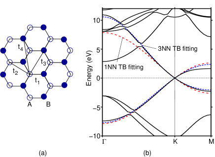
For the freestanding monolayer graphene, it is known that the formation of the Dirac cones at the Fermi surface is the outcome of the pz-pz hopping between the two inequivalent carbon atoms A and B in the unit cell. Though a simple tight-binding model involving the pz-pz interaction within the nearest neighbor (NN) coordination explains the linear band dispersion at the Dirac points K and K′, it is essential to include further neighbor hoppings if an accurate description of the band structure in the entire Brillouin zone is desired. We find that for this, al least three NN hopping integrals must be retained as indicated from the root-mean-square deviation given in Table 1 and the band structure of Fig. 2.
The TB Hamiltonian is a 2 2 matrix
| (3) |
where A and B denote the two carbon atoms in the unit cell. Retaining only the first two NN hoppings, the form of the matrix elements are
and . This can be easily generalized to further near neighbors. The symbols , , , and are the NN hopping parameters as shown in Fig. 2, ‘a’ is the C-C bond length, and the on-site energy of the carbon orbital is taken to be zero. The slope of the Dirac cone centered at the K or the K′ point, easily obtained by diagonalizing the Hamiltonian and taking the limits, is given by the expression
| (5) |
The slope at the Dirac point is about Å, as calculated from LAPW, which corresponds to the velocity of m/sec. The TB bands were fitted to the LAPW bands by keeping hopping integrals for a certain number of NNs and neglecting the hopping for further neighbors. We obtained two sets of optimized parameters. The first set of TB parameters was obatined by constraining the slope of the linear bands at the Dirac point to the LAPW value, while the second set was obtained without this constraint. For low energy properties, where the magnitude of the slope may be important, the second set of the parameters should be used. The results are shown in Fig. 2 and Table I. In our TB work of the BLG below, we have retained only the first NN interaction with the slope constraint, since this is sufficient for our purpose as we are mainly interested in states close to the band gap region.
| Range of | t1 | t2 | t3 | t4 | RMS |
|---|---|---|---|---|---|
| hopping | (eV) | deviation | |||
| Without Slope Constraint | |||||
| 1NN | -2.625 | 0.42 | |||
| 2NN | -2.910 | 0.160 | 0.22 | ||
| 3NN | -2.840 | 0.170 | -0.210 | 0.11 | |
| 4NN | -2.855 | 0.170 | -0.210 | 0.105 | 0.10 |
| With Slope Constraint | |||||
| 1NN | -2.56 | 0.46 | |||
| 2NN | -2.56 | 0.160 | 0.32 | ||
| 3NN | -2.90 | 0.175 | -0.155 | 0.12 | |
| 4NN | -2.91 | 0.170 | -0.155 | 0.02 | 0.115 |
III Bilayer Graphene in the Hexagonal structure
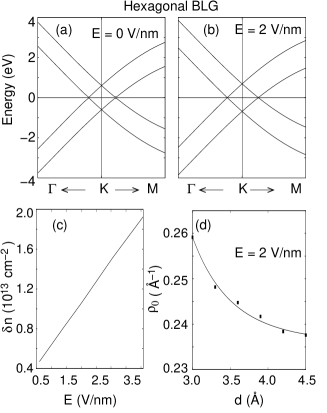
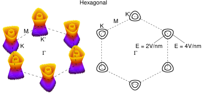
As mentioned already, recent experiments suggest that the hexagonal BLG is surprisingly commonhoriuchi in spite of its higher energy as obtained from the total energy calculation (Fig. 1 and Ref. 17) that indicate the Bernal BLG to be higher than the hexagonal BLG by 5 meV/C atom. For the equilibrium interlayer spacing (d = 3.51 Å), the band structure for the hexaoganal stacked BLG is shown in Fig. 3(a) and the topology of the bands near the Fermi surface is shown in Fig. 6. Unlike the case of the Bernal stacked BLG, here we see two interpenetrating Dirac cones, which intersect to form a circular Fermi surface, the Dirac circle.
An electric field does not change the overall feature of the band structure (see Fig. 3(b)) and in contrast to the Bernal BLG, it does not produce a band gap because of the higher symmetry situation in the hexagonal stacking. The main features of the band structure can be understood from a tight-binding (TB) model involving the nearest-neighbor - interaction of the pz orbitals in the graphene plane and the - interaction between the planes. With the four inequivalent carbon sites, one can form the Hamiltonian as in the monolayer case and in addition add the interlayer coupling term. One can then expand the Hamiltonian matrix elements for a small momentum around the Dirac point, which then becomes an excellent approximation for the band gap region. The result is
| (10) |
where is the Fermi velocity for the monolayer, is the complex momentum with respect to the Dirac point K, is the potential difference between the two layers, is the interlayer hopping integral ( as extracted from the LAPW results), and the basis set of the Hamiltonian consists of the Bloch functions made out of the carbon orbitals located at A, , , and B, respectively and in that order. The atoms are indicated in Fig. 1. The electric field potential appearing in the Hamiltonian Eq. 10 corresponds to the final screened field experienced by the electrons and not to the bare electric field which is reduced by the polarization field due to screening, so that , where is the external electric field and is the static dielectric constant.
The Hamiltonian is easily diagonalized to yield the eigenvalues
| (11) |
where
| (12) |
specifies the energy locations of the vertices of the Dirac cones. The energy dispersion is sketched in Fig. 6, which shows the two Dirac cones with linear dispersion with the vertices of the cones separated by the energy .
The radius of the circular Fermi surface, the “Dirac” circle, where the cones intersect the zero of energy, is simply Since for small fields the screened potential is proportional to the applied field, the equation indicates that increases both with the applied electric field and the interlayer hopping parameter ( increases as the interlayer separation decreases). This is a notable feature of the hexagonal BLG, viz., that we have a circular Fermi surface with zero band gap and that the radius of the circle can be modified by electric field and strain. Any doped holes or electrons will form a thin shell in the momentum space around the Dirac circle. This may lead to interesting electronic and magnetic properties in the presence of impurities.
IV Bilayer Graphene in the Bernal Structure
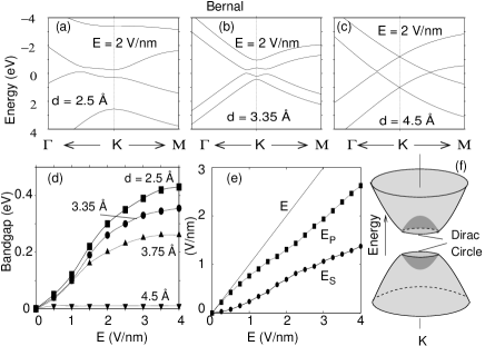
The effect of strain and electric field on the band structure of the Bernal BLG is summarized in Fig. 5. As seen from Fig. 1(a), for the Bernal BLG, there are four nearly parabolic bands near the Fermi energy and two of these touch at the Dirac point making it a zero band-gap semiconductor. However, in the presence of an electric field, these two bands split opening up a small gap (Fig. 5(b)) consistent with earlier density functional resultsguo ; raza . The magnitude of the band gap increases linearly for small electric fields and saturates for higher electric fields as seen from Fig. 5(d).
For large interlayer spacing, there is very little coupling between the two individual sheets and the bands for the single graphene sheet are reproduced (Fig. 5(d)). If the interlayer separation is large enough ( 4.5 Å), the gap vanishes irrespective of the electric field and decreasing the magnitude of increases the gap substantially. Quite interestingly, if is too small ( 2.7 Å), the band gap becomes indirect due to interactions with other orbitals in addition to pz. However, the indirect band gap may not be realized in practice because of the large strain needed, which may also lead lead to a possible deformation of the graphene sheets. For reasonable layer separations, the electric field produces a small direct gap at k points, the locus of which is nearly a circle (the “Dirac” circle) centered around the K or the K′ points in the Brillouin zone as indicated from the band structure of Fig. 5(b) and Fig. 4.
The main features of the band structure can again be explained by a nearest-neighbor TB model, analogous to the case for the hexagonal structure. The resulting Hamiltonian is
| (17) |
where the basis set of the Hamiltonian consists of the Bloch functions made out of the carbon orbitals located at A, , , and B, in that order. Diagonalization of the Hamiltonian yields the four eigenvalues
| (18) | |||||
At the K or the K′ points in the Brillouin zone, the energies of the bands are , and they disperse quadratically as seen from Fig. 5(b) such that a gap of magnitude is produced at k points in the Brillouin zone that make the “Dirac circle” of radius . The above expression clearly shows that Eg increases linearly for low fields and saturates at high fields (). This is consistent with the density-functional results for the dependence of the band gap on the external field and bilayer spacing shown in Fig. 5(d).
V Screening in the BLG
It has already been pointed out that the screening is divergent in the Bernal structure for small applied fields between the layers,mccann1 ; min which is a consequence of the band topology at low energies. In this Section, we examine the screening in the hexagonal structure and compare with the results for the Bernal structure. An applied electric field transfers electrons from one graphene layer to the other, which produces a polarization field resulting in the net screened field that the electrons see, so that we have .
We compute the screening effects in three different ways using (a) density-functional LMTO method, (b) the tight-binding model, and finally (c) from an analytic expression obtained by using the linear band dispersion. Unlike the Bernal structure, we find that the screening does not diverge in the hexagonal structure.
In the LMTO calculations, an extra potential was added to the on-site energies of the carbon orbitals of the two layers of BLG and the band structure was determined self-consistently. The screened potential can then be directly obtained from the final on-site energies of the carbon orbitals by examining the band-center energies. For this purpose, the C 2s orbital is especially useful, since it acts like a core orbital.
For the TB as well as the analytic calculation, we computed the polarization field by approximating the induced charges in the graphene layer by a uniform sheet charge density , which turns out to be an excellent approximation for computing the screening. The polarization field is then given from the Gauss’ Law in electrostatics to be , so that
| (19) |
where is the difference between the sheet carrier density of the two graphene layers and is the dielectric constant. In terms of the electric potential the above equation can be wrtitten as
| (20) |
where is the interlayer separation. One can obtain the value of from the normalized eigenfunctions of the BLG Hamiltonian.
Diagonalizing the Hamiltonian for the hexagonal BLG (Eq. 10), the eigenfunctions corresponding to the upper and the lower Dirac cones, centered at and respectively, are found to be
| (21) |
where , and the sign inside the ket indicates the upper and the lower band and denotes the upper (lower) Dirac cone. Denoting the four components of the wave function by , , , and (from top to bottom), corresponding to the appropriate Bloch functions, the surface electron density is given by
| (22) |
where Acell is the unit cell area, is the band index, the superscript 1(2) refers to the two individual layers, and the factor of two in front of the summation takes care of the electron spin.
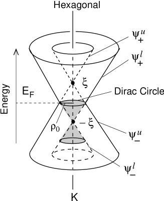
The summation in Eq. 22 need to be performed only over the shaded region in Fig. 6, since we are interested only in the difference . The remaining portions of the two occupied bands and cancel each other’s contribution at each point to this difference as can be easily verified from Eqs. (21) and (22). The net result is then
| (23) |
where the summation goes over the two bands below and the integration goes up to the radius of the Dirac circle, so that the contribution comes only from the shaded region of Fig. 6. The factor of four in Eq. 23 was inserted to account for both the spin degeneracy and the two Dirac valleys in the Brillouin zone at the K and K′ points. Using the wave functions Eq. 21, the integration is easily performed to yield
| (24) |
Now, electrons of course see the screened field, so that the net charge density difference between the layers is obtained by using the screened potential in lieu of in the expression (24). This together with Eq. 20 yields the ratio between the external potential and the screened potential, which is
| (25) |
This is plotted in Fig. 25 together with the LMTO result and the TB result. The latter was obtained by a full self-consistent calculation using the nearest-neighbor tight-binding model, from which the charge difference was computed and used in Eq. 20 to obtain the ratio of . In the LMTO results, all electrons including the carbon electrons participated in the screening, while in the analytical and TB calculation, which included the effects of only the electrons, we replaced, for simplicity, just the vacuum dielectric constant for appearing in Eq. 25.

Fig. 7 shows the calculated results for the screening for both the hexagonal and the Bernal structures. For both cases, screening increases with applied electric field, except for the divergence at low field for the Bernal structure as has been pointed out earlier. The increase of screening with increasing field is due to the fact that proportionately more carriers become involved in screening as the density-of-states for the linear bands near the Fermi energy increase as square of energy. The analytic and the TB results agree quite well, which is not surprising since the energy spectrum differs only beyond the linear region of the bands and these states don’t contribute much because they are far away from the Fermi energy. The density-functional LMTO result, on the other hand, shows larger screening because it includes all carbon electrons that participate in screening.
For the Bernal structure, the divergent screening for low fields may be explained due to the relatively flat bands at the Fermi energy (see Fig. 1 a). The effects of the two flat bands touching at the Fermi energy may be taken into account by constructing a effective Hamiltonian using perturbation theory from the full Hamiltonian of Eq. 17 and then computing the magnitude of the charge difference from the eigenfuctions. This can be done analytically and, for low fields, the result ismccann1 ; min
| (26) |
where and the cutoff momentum Å-1. This result has been plotted in Fig. 7 for the Bernal structure and it explains the calculated trend in the density-functional results.
VI Summary
In summary, we have studied the effect of the electric field and strain on the electronic structure of hexagonal and Bernal stacked bilayer graphene. While a gap opens up in the Bernal structure BLG by the application of an external electric field, the hexagonal BLG remains a zero-gap metal, but with an interesting circular Fermi surface, the Dirac circle, that can be controlled by both strain and electric field. Any doped electrons or holes will occupy a thin shell in the Brillouin zone, which leads to an interesting Fermi surface in the doped system.
This work was supported by the U. S. Department of Energy through Grant No. DE-FG02-00ER45818.
References
- (1) T. Ohta, A. Bostwick, T. Seyller, K. Horn, and E. Rotenborg, Science 313, 951 (2006).
- (2) J. B. Oostinga, H. B. Heersche, X. Liu, A. F. Morpurgo, and L. M. K. Vandersypen, Nature Mater. 7, 151 (2008).
- (3) S. Latil and L. Henrard, Phys. Rev. Lett. 97, 036803 (2006).
- (4) E. McCann and V. I. Fal’ko, Phys. Rev. Lett. 96, 086805 (2006).
- (5) E. McCann, Phys. Rev. B 74, 161403(R) (2006).
- (6) E. V. Castro, K. S. Novoselov, S. V. Morozov, N. M. R. Peres, J. M. B. Lopes dos Santos, J. Nilsson, F. Guinea, A. K. Geim, and A. H. Castro Neto, Phys. Rev. Lett. 99, 216802 (2007).
- (7) H. Min, B. Sahu, S. K. Banerjee, and A. H. MacDonald, Phys. Rev. B 75, 155115 (2007).
- (8) J. Nilsson and A. H. Castro Neto, Phys. Rev. Lett. 98, 126801 (2007).
- (9) S. Horiuchi, T. Gotou, M. Fujiwara, R. Sotoaka, M. Hirata, K. Kimoto, T. Asaka, T. Yokosawa, Y. Matsui, K. Watanabe, and M. Sekita, Jpn. J. Appl. Phys. 42, L1073 (2003).
- (10) Z. Liu, K. Suenaga, P. J. F. Harris, and S. Iijima, Phys. Rev. Lett. 102, 015501 (2009).
- (11) T. Ohta, A. Bostwick, J. L. McChesney, T. Seyller, K. Horn, and E. Rotenberg, Phys. Rev. Lett. 98, 206802 (2007).
- (12) F. Varchon, R. Feng, J. Hass, X. Li, B. N. Nguyen, C. Naud, P. Mallet, J.-Y. Veuillen, C. Berger, E. H. Conrad, and L. Magaud, Phys. Rev. Lett. 99, 126805 (2007).
- (13) Y. Guo, W. Guo, and C. Chen, Appl. Phys. Lett. 92, 243101 (2008).
- (14) H. Raza and E. C. Kan, J. Phys.: Condens. Matter 21, 102202 (2009).
- (15) O. K. Andersen and O. Jepsen, Phys. Rev. Lett. 53, 2571 (1984).
- (16) P. Blaha et al., WIEN2k, ”An Augmented Plane Wave + Local Orbitals Program for Calculating Crystal Properties” (Karlheinz Schwarz, Techn. Universitat Wien, Austria, 2001) ISBN.
- (17) S. Shallcross, S. Sharma, and O. A. Pankratov, J. Phys.: Condens. Matter 20, 454224 (2008).