Omni-directional, broadband and polarization-insensitive thin absorber in the terahertz regime
Abstract
A nearly omni-directional THz absorber for both transverse electric (TE) and transverse magnetic (TM) polarizations is proposed. Through the excitation of magnetic polariton in a metal-dielectric layer, the incident light is perfectly absorbed in a thin thickness which is about times smaller than the resonance wavelength. By simply stacking several such structural layers with different geometrical dimensions, the bandwidth of this strong absorption can be effectively enhanced due to the hybridization of magnetic polaritons in different layers.
pacs:
78.20.Ci, 77.22.Ch, 41.20.-qI Introduction
High absorption in a thin film is of critical importance in some device applications such as micro bolometers Mauskopf , thermal detectors Parsons and solar cells Rand ; Pillai , whose working spectra are from infrared to optical frequencies. Several absorbing structures have been proposed previously. For instance, a bare metallic grating can fully absorb the incident light at some well defined wavelengths Hutley ; Collin ; Tan ; Popov . However, absorption in metallic gratings usually relies on delocalized surface excitations Bliokh , which are highly sensitive to the angle of incidence. This narrow-angle absorption prevents their application to e.g. photovoltaic cells, where wide collection angles are necessary. Another widely used method is based on structured metal-dielectric interfaces, such as Dallenbach layers Reinert ; Knott and Salisbury screens Salisbury ; Engheta , which can give frequency-selective absorption of incident light. However, these types of structures often limited to a minimal thickness of one quarter wavelength. Recently, Landy et al. proposed an innovative metal-dielectric composite named metamaterial absorber to overcome this thickness limitation Landy1 ; Tao1 . Later, some efforts have been made on this metamaterial absorber to achieve polarization-insensitive absorption Landy2 or wide-angle (only in the incident plane with a fixed azimuthal angle) absorption Tao2 ; Avitzour . The above-mentioned absorbing structures have shown their great ability for light absorption. However, omni-directional absorption (i.e., wide-angle absorption for any azimuthal angle) in a thin film (much thinner than one quarter wavelength) for incident wave of both polarizations remains a challenge. Moreover, most of these designs are based on strong electromagnetic resonances to effectively absorb the incident light in a thin thickness, especially for a metamaterial absorber, and consequently the bandwidth of this resonant absorption is often narrow, typically no more than with respect to the center frequency. This narrow bandwidth feature of the resonant absorption limits the device applications of these absorbing structures.
This paper is dedicated to the design of an omni-directional and broadband thin absorber for both polarizations in terahertz frequency range ( ), where it is difficult to find naturally occurring materials with very strong absorption Williams ; Tonouchi . We numerically demonstrate that a composite structure of a cut-wire array, a lossy polymer separation layer and a metal ground film can be used as an effective absorber with a resonant absorption up to when the thickness of the separation layer is properly designed. Moreover, by simply replacing the cut-wires with crosses, nearly omni-directional absorption is achieved in this more symmetric composite structure for both TE and TM polarizations. Most importantly, we successfully demonstrate that, by stacking these layers of metallic crosses with different geometrical dimensions, several closely positioned resonant peaks are merged in the absorption spectrum due to the hybridization of the magnetic polaritons, and consequently the bandwidth is effectively enhanced.
II Wide angle absorption of a composite cut-wire structure
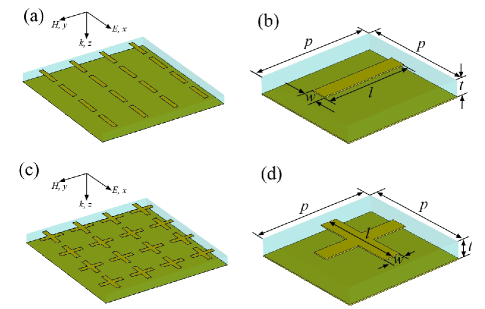
First we study a simplified composite structure which is made of a metallic cut-wire array positioned above a metallic film (with a polymer layer in between) as depicted in Fig. 1(a). A lossy polymer with dielectric is used in our numerical simulation. The thickness of the polymer layer is adjustable, the width and length of the cut-wire are and , respectively. As shown in Fig. 1(b), the length of the unit cell (i.e., the period of the cut-wire array) in both x and y directions are . In the simulation, the metallic structures were made of lossy gold with a conductivity of and a thickness of . As the thickness of the metallic film used here is much larger than the typical skin depth in the THz regime (to avoid transmission through the metallic film), the reflection is the only factor limiting the absorption. Here we consider the case when a plane wave [with electric field polarized in x direction; see Fig. 1(a)] normally impinges on the structure. By using a Finite-Integration Time Domain algorithm CST , the reflection spectra for different separation distances are calculated and shown in Fig. 2(a). In each reflection spectrum shown in Fig. 2(a), one sees a significant resonant dip where the reflection drops rapidly. To obtain a physical insight, the distributions of the z-component electric field on the cut-wire and the metallic film are shown in Fig. 2(c) and (d), respectively, for resonance A [see Fig. 2(a)] as an example. As shown in Fig. 2(c), charges of opposite signs accumulate at the two ends of the cut-wire, indicating the excitation of an electric dipole resonance on the cut-wire. This electric dipole is greatly coupled with its own image, which oscillates in anti-phase on the metallic film [see Fig. 2(d)]. Consequently, a magnetic polariton (or ”magnetic atom”) liu1 ; Li is formed, which induces a strong magnetic response (see Fig. 6(a) below) and causes a resonant dip in the reflection spectrum liu2 . The coupling strength of the electric dipoles as well as the magnetic response is mainly determined by the separation distance. By tuning the thickness of the spacer layer, we can obtain an optimal value , at which the electric and magnetic response makes the composite structure impedance-matched to the free space, and the reflection is considerably suppressed () at resonant frequency , as shown by the black curve in Fig. 2(a). of the incident wave is effectively absorbed in the composite structure with a thickness of less than . To give a further interpretation, an LC-circuit model, as shown in the inset of Fig. 2(a), is introduced to approximately describe this magnetic polariton caused resonance. Each of the two capacities is formed by the metallic film and an upper or lower half of the cut-wire. The capacitance can be described approximately by a two-plate capacitor formula Zhou . The inductance L of the structure is approximately given by (as for the case of two parallel plates). Then the resonant frequency is given by:
| (1) |
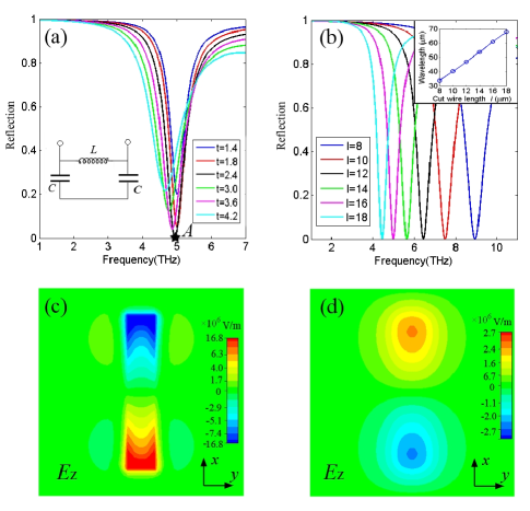
From Eq. (1), we can deduce that the resonant frequency is not sensitive to the change of separation distance . This agrees well with our simulation results (the resonant peaks are at similar frequencies), as illustrated in Fig. 2(a). The reflection spectra for different lengths of the cut-wire are also shown in Fig. 2(b). Compared with Fig. 2(a), a significant redshift of the resonant peak (with little change in amplitude) is observed when increases from to . The linear dependence of the resonant wavelength on cut-wire length is demonstrated in the inset of Fig. 2(b), as predicted by Eq. (1).
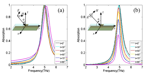
Next we study the resonant absorption behavior for the case of optimal thickness , when the incident angle increases. Figs. 3(a) and 3(b) give the absorption spectra when incident angle varies from to in TM configuration (i.e., H-field is fixed along the y direction) and TE configuration (E-field is fixed along the x direction), respectively. For the case of TM configuration, as the incident angle increases, the amplitude of the absorption peak decreases slightly but still keeps above [see Fig. 3(a)] even when , at which angle the electric field is nearly normal to the cut-wire. Thus we can conclude that the magnetic polariton, which causes the resonant absorption in the composite structure, is effectively excited by the y-component of the magnetic field, while the x-component of the electric field (which can drive the electric dipole oscillation on the cut-wire) contributes a little. Meanwhile, a blueshift of the absorption peak occurs (see Fig. 3(a)), which is relatively small ( ) for , and reach when increases to . It is not difficult to understand this blueshift for the obliquely incident light. As we know, for the normal incident case, the electric dipole of the cut-wire [see Fig. 2(a)] in each unit cell oscillates in phase. Accordingly, the attractive force of the opposite charges of the adjacent cut-wires in x direction reduces the restoring force of the charge oscillation inside the cut-wire. Compare with a single cut-wire, the resonant frequency of the cut-wire array is reduced due to this interaction between the neighboring unit cells. (Our numerical simulation has shown that this small redshift of the absorption peak will be reduced when the period increases, i.e., the interaction between the neighboring unit cells decreases.) However, as the incident angle increases for the TM configuration [see the inset of Fig. 3(a)], the dipole oscillation of the adjacent cut-wires in x direction is no longer in phase, which causes the reduction of the attractive force between these adjacent cells, and consequently the absorption peak moves slightly to a higher frequency. For the TE configuration, a distinct amplitude reduction of absorption peak is observed as the incident angle increases [see Fig. 3(b)]. However, for small incident angle , the absorption spectrum are almost overlapped with the one for normal incidence. A high absorption of at resonant frequency is still achieved when . Beyond this angle, the amplitude of the absorption peak drops quickly, as the y-component of the incident magnetic field decreases rapidly to zero and can no longer efficiently excite this magnetic polariton. Compared with the TM configuration, here the frequency shift of the absorption peak is really small (almost imperceptible), since the coupling of the adjacent unit cells in y direction is relatively small due to the larger spacing. Notably, the present simulation results demonstrate that this simplified structure can have quite wide angle absorption for both TE and TM configurations, which is similar to the composite structure (of electric inductive-capacitive resonators and a metallic film) used in Ref. Tao2 .
III Omni-directional and polarization-insensitive absorption in a composite structure of metallic crosses
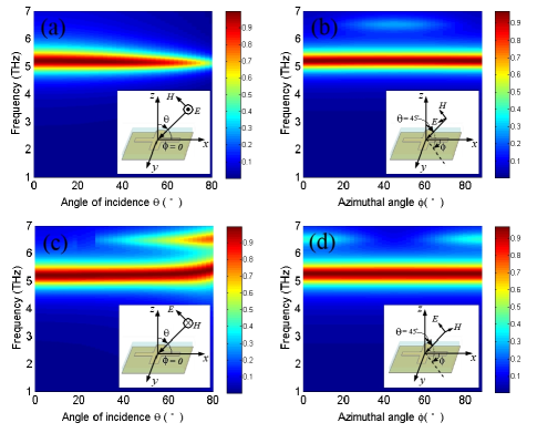
Although the resonant absorption of the composite structure of cut-wires can work over a wide range of incident angles , the effective absorption can be obtained only for a plane wave without x-component of magnetic field. However, due to the structural simplicity, the above absorber can be easily extended to a more symmetric structure in order to highly absorb the plane wave with x-component of the magnetic field. We demonstrate this by simply replacing the cut-wire array with the cross array as shown in Fig. 1(c) and (d). The unit cell for the numerical calculation is depicted in Fig. 1(d). The cross here is composed of two orthogonally intersected cut-wires of same size. The width and length of the constitutive cut-wire are the same as those used in Fig. 1, while the optimal thickness of the separation layer is adjusted to (slightly different from the previous value) in order to be impedance-matched to the free space. Fig. 4(a) and (c) show the absorption spectra as a function of the incidence-angle for TE and TM waves, respectively, when the azimuthal angle is fixed to 0. The propagation and the polarization direction of the incident wave are shown in the inset of each figure. From Fig. 4(a) and (c) one can see that the present absorber can still work over a wide range of incident angle (as for the case of the composite cut-wire structure (see Fig. 3)] for both TE and TM polarizations, because the additional constitutive cut-wire, which is normal to the electric field and parallel to the plane of magnetic field, has no resonant electromagnetic response, and consequently has little influence on the excitation of magnetic polariton. Moreover, for any fixed incident angle , the resonant absorption of this more symmetric structure is quite isotropic in the x-y plane (as the azimuthal angle varies) as illustrated in Fig. 4(b) and (d) for TE and TM waves, respectively (here we choose incident angle as an example). The insensitivity to the azimuthal angle variation is not difficult to understand. Any incident plane wave impinging on this composite structure can be decomposed into two components with the magnetic field in x-z or y-z plane. At resonant frequency, each component can effectively excite the corresponding magnetic polariton (between one constitutive cut-wire and the metallic film), and then will be greatly absorbed. Our simulation results reveal that the present composite structure of metallic crosses gives nearly omni-directional and polarization-insensitive absorption as the case in Ref. Teperik . However, compared with the absorbing structure of nanocavities in gold substrate proposed in Ref. Teperik , the present structure is much thinner (), and can be easily manufactured with standard planar micro-fabrication techniques Boltasseva .
IV Broadband absorption of a multi-layer structure
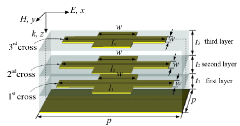
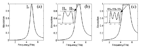
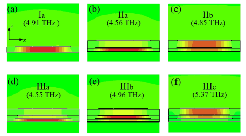
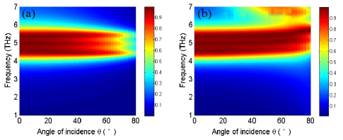
Below we try to increase the bandwidth of the absorption by using a multi-layer structure which can support several resonant modes closely positioned in the absorption spectrum. From Eq. (1), the resonant frequency of the absorption caused by the magnetic polariton is primarily determined by wire length . Thus in different layers we design crosses of slightly different lengths to ensure that the resonance frequencies of magnetic polaritons could be close to each other. Then, by tuning the polymer separation thickness of each layer, the multi-layer structure can be impedance-matched to the free space at each resonant frequency (similar to the one-layer case shown in Fig. 2(a)). In Fig. 5, we show as an example the schematic diagram of a 3-layer cross structure, which consists of three alternating layers of gold crosses and polymer separation layers, and a gold film at the bottom. The geometric parameters of each cross/ polymer layer are marked in Fig. 5. The crosses from the bottom to the top are denoted in sequence as the cross, cross, cross. In the present design for 1-, 2-, or 3-layer structure, wire width is equal (for simplicity) and fixed to for all the crosses. The other geometrical parameters for different layers of the structure are optimized and given in Table 1. The corresponding absorption spectra for normally incident plane wave with electric field in x direction (see Fig. 5) are simulated and presented in Fig. 6(a), (b), (c). For the sake of clarity, we first study the case of 2-layer structure. Different from the case of the 1-layer structure with single resonance (Ia), two closely positioned resonances with absorption up to are clearly observed in the inset of Fig. 6(b). One resonance (IIa) is at frequency , while the other resonance (IIb) is at frequency . To understand the origin of the spectral characteristics, the distributions of y-component magnetic field magnitude in plane (see Fig. 5) at the two resonances are shown in Fig. 7(b) and (c). As Fig. 7(b) shows, resonance IIa of lower frequency is primarily associated with the excitation of magnetic polariton in the first layer, which is caused by the electric dipole coupling between the 1st cross and the metallic film [like the case of 1-layer structure, see Fig. 7(a)], while only a small magnetic response can be observed in the second layer at this frequency. For resonance IIb, strong magnetic field is found in both the first and second layers as shown in Fig. 7(b), which means that the magnetic polariton of each layer contributes significantly to this resonant absorption. Thus resonance IIb can be regarded as a hybridized mode liu1 ; liu2 of two magnetic polaritons strongly coupled to each other. Due to the great contribution from the magnetic polariton of the second layer, resonance IIb shifts slightly to a higher frequency as compared with resonance IIa. Owing to these two closely positioned resonant peaks, we obtain a relatively wide frequency band (from 4.45 to 4.95 ) of absorption, where nearly perfect absorption (more than ) occurs. The full bandwidth at half maximum (FWHM) of the absorption is greatly improved to (with respect to the central frequency), which is almost two times larger than that of the 1-layer structure. Taking a step further, we demonstrate a broader bandwidth absorption in a three-layer structure in Fig. 6(c). By stacking one more layer, additional magnetic polariton is introduced to this hybridization system. Accordingly, three closely located resonances (IIIa, IIIb, IIIc) are observed at frequencies , 4.96 and 5.37 , as shown in the inset of Fig. 6(c). The corresponding distributions of y-component magnetic field magnitude on plane are also shown in Fig. 7(d), (e), (f). Each resonance is a hybridized mode contributed differently by the three magnetic polaritons of the three layers. In this 3-layer cross structure, a frequency band ( ) with nearly perfect absorption (more than ) is achieved, and the FWHM of the absorption increases to 1.9 , which is nearly of the central frequency. Meanwhile, the thickness of the 3-layer structure is still quit thin (no more than ). Importantly, the wide-angle feature of this high absorption caused by the magnetic polariton is preserved in this multi-layer structure as shown in Fig. 8(a), (b) for TE and TM waves, respectively. The absorption variation with the change of the azimuthal angle is not given here, as the stacking of layers in z-direction does not spoil the structural symmetry in the x-y plane [consequently the isotropic absorption in the x-y plane can be obtained just like the case of single layer, see Fig. 4(b), (d)]. A further broadening of the absorption bandwidth is also possible by increasing the number of stacked layers.
| 1-layer | 17 | 1.6 | 6 | ||||
|---|---|---|---|---|---|---|---|
| 2-layer | 17 | 16.5 | 0.9 | 2.2 | 6 | ||
| 3-layer | 17 | 15.4 | 15 | 0.7 | 1.1 | 2.0 | 6 |
V Conclusion
In summary, we have designed a thin THz absorber with a thickness smaller than , and achieved a high absorption which is nearly omni-directional for both TE and TM polarizations. A simplified LC model has been introduced to elucidate the resonant behavior. The wide angle nature of the resonant absorption has been carefully analyzed. Moreover, we have successfully demonstrated that the bandwidth of the absorption can be effective improved by using multi-layer structure, while the wide angle feature remains. The proposed multi-layer structure can be easily fabricated through a layer-by-layer technique Qi ; Subramania ; Chang , and allows for easy integration with various devices. This omni-directional THz absorber, which is also polarization-insensitive and broad band, has potential applications in e.g. thermal detectors and THz imaging.
Acknowledgements.
The authors would like to acknowledge the partial support of National Basic Research program (973 Program) of China under Project No.2004CB719800 and a Swedish Research Council (VR) grant on metamaterials.References
- (1) P. D. Mauskopf, J. J. Bock, H. Del Castillo, W. L. Holzapfel, and A. E. Lange, Appl. Opt. 36, 765 (1997).
- (2) A. D. Parsons and D. J. Pedder, J. Vac. Sci. Technol. A 6, 1686 (1988).
- (3) B. P. Rand, P. Peumans, and S. R. Forrest, J. Appl. Phys. 96, 7519 (2004).
- (4) S. Pillai, K. R. Catchpole, T. Trupke, and M. A. Green, J. Appl. Phys. 101, 093105 (2007).
- (5) M. C. Hutley, and D. Maystre, Opt. Commun. 19, 431 (1976).
- (6) S. Collin, F. Pardo, R. Teissier, and J. L. Pelouard, Appl. Phys. Lett. 85, 194 (2004).
- (7) W. C. Tan, J. R. Sambles, and T. W. Preist, Phys. Rev. B 61, 13177 (2000).
- (8) E. Popov, L. Tsonev, and D. Maystre, Appl. Opt. 33, 5214 (1994).
- (9) Y. P. Bliokh, J. Felsteiner, and Y. Z. Slutsker, Phys. Rev. Lett. 95, 165003 (2005).
- (10) J. Reinert, J. Psilopoulos, J. Grubert, and A. F. Jacob, Microw. Opt. Technol. Lett. 30, 254 (2001).
- (11) E. F. Knott, J. F. Schaeffer, and M. T. Tuley, in Radar Cross Section, edited by A. House, 2nd ed. (Artech House, Norwood, MA, 1993).
- (12) Salisbury, U.S. Patent No. 2,599,944 (1952).
- (13) N. Engheta, IEEE AP-S Int. Symp. Dig., 2, 392 (2002).
- (14) N. I. Landy, S. Sajuyigbe, J. J. Mock, D. R. Smith and W. J. Padilla, Phys. Rev. Lett. 100, 207402 (2008).
- (15) H. Tao, N. I. Landy, C. M. Bingham, X. Zhan, R. D. Averitt, and W. J. Padilla, Opt. Express 16, 7181 (2008).
- (16) N. I. Landy, C. M. Bingham, T. Tyler, N. Jokerst, D. R. Smith, and W. J. Paddila, Phys. Rev. B 79, 125104 (2009).
- (17) H. Tao, C. M. Bingham, A. C. Strikwerda, D. Pilon, D. Shrekenhamer, N. I. Landy, K. Fan, X. Zhang, W. J. Padilla, and R. D. Averitt, Phys. Rev. B 78, 241103 (2008).
- (18) Y. Avitzour, Y. A. Urzhumov, and G. Shvets, Phys. Rev B 79, 045131 (2009).
- (19) G. P.Williams, Rep. Prog. Phy. 69, 301-326 (2006).
- (20) M. Tonouchi, Nat. Photonics 1, 97-105 (2007).
- (21) T. V. Teperik, F. J. Garcia De Abajo, A. G. Borisov, M. Abdelsalam, P. N. Bartlett, Y. Sugawara and J. J. Baumberg, Nat. Photonics 2, 299 (2008).
- (22) All the simulations in this paper are performed using software package CST Microwave Studio, CST GmbH, Germany.
- (23) N. liu, L. Fu, S. Kaiser, H. Schweizer, and H. Giessen, Adv. Mater. 20, 3859 (2008).
- (24) N liu, H. Guo, L, Fu, S. Kaiser, H. Schweizer, and H. Giessen, Adv. Mater. 19, 3628 (2007).
- (25) T. Li, H. Liu, F. M. Wang, Z. G. Dong, S. N. Zhu, and X. Zhang, Opt. Express 14, 11155 (2006).
- (26) J. Zhou, L. Zhang, G. Tuttle, T. Koschny, and C. M. Soukoulis, Phys. Rev. B 73, 041101 (2006).
- (27) A. Boltasseva, and V. M. Shalaev, Metamaterials 2, 1-17 (2008).
- (28) M. Qi, E. Lidorikis, P. T. Rakich, S. G. Johnson, J. D. Joannopoulos, E. P. Ippen, and H. I. Smith, Nature 429, 538-542 (2004).
- (29) G. Subramania, and S. Y. Lin, Appl. Phys. Lett. 85, 5037-5039 (2004).
- (30) A. S. P. Chang, Y. Kim, M. Chen, Z. Yang, J. A. Bur, S. Lin, and K. Ho, Opt. Express 15, 8428-8437 (2007).