Corresponding author: S. Burger
URL: http://www.zib.de/Numerik/NanoOptics/
Email: burger@zib.de
Benchmark of Rigorous Methods
for Electromagnetic Field Simulations
Abstract
We have developed an interface which allows to perform rigorous electromagnetic field (EMF) simulations with the simulator JCMsuite and subsequent aerial imaging and resist simulations with the simulator Dr.LiTHO. With the combined tools we investigate the convergence of near-field and far-field results for different DUV masks. We also benchmark results obtained with the waveguide-method EMF solver included in Dr.LiTHO and with the finite-element-method EMF solver JCMsuite. We demonstrate results on convergence for dense and isolated hole arrays, for masks including diagonal structures, and for a large 3D mask pattern of lateral size 10 microns by 10 microns.
keywords:
3D rigorous EMF simulations, lithography simulations, microlithography, finite-element method, waveguide methodThis paper will be published in Proc. SPIE Vol. 7122, 71221S (2008), (Photomask Technology 2008, Hiroichi Kawahira; Larry S. Zurbrick, Eds., Society of Photo-Optical Instrumentation Engineers, 2008) and is made available as an electronic preprint with permission of SPIE. One print or electronic copy may be made for personal use only. Systematic or multiple reproduction, distribution to multiple locations via electronic or other means, duplication of any material in this paper for a fee or for commercial purposes, or modification of the content of the paper are prohibited.
1 Introduction
Support from modeling and simulation is critical to push the limits of traditional optical lithography. A specific requirement for lithography modeling and simulation is the need for very efficient electromagnetic field (EMF) solvers that allow the simulation of large 3D computational domains [1]. We have developed an interface between the lithography simulator Dr.LiTHO and the program package JCMsuite for EMF simulations. Dr.LiTHO is a comprehensive simulation environment for photolithography developed at the Fraunhofer IISB. The included EMF simulators are based on the waveguide method [2] and on the FDTD method. JCMsuite is a finite element based solver for EMF simulations developed at JCMwave and at the Zuse Institute Berlin [3, 4, 5]. Both solvers allow the rigorous simulation of relatively large 3D computational domains. The interface between the program packages enables the accuracy benchmarking of the results obtained with the EMF simulators of Dr.LiTHO and JCMsuite.
We quantitatively compare the near field results (complex diffraction coefficients) obtained with the waveguide method and with the finite element method. Then the resist images resulting from the mask near fields are computed with the fully vectorial imaging system of Dr.LiTHO. We also compare the resist images corresponding to the near field results obtained with the respective EMF solvers regarding process windows and CDs.
We investigate several application examples: (a) isolated and dense contact holes with target CD’s of 65 nm and 45 nm. (b) Z-like structures in order to get a combination of horizontal, vertical and 45-degree rotated elements which are critical from the simulation point of view, and (c) a larger more complex patterned mask area with a size of 10 microns x 10 microns. For all simulations we consider state of the art mask types and lithography settings.
2 Background
2.1 Dr.LiTHO
Dr.LiTHO is a comprehensive simulation environment for photolithography, developed at the Fraunhofer IISB.111 URL: http://www.drlitho.com Its main focus is on development and research applications. Dr.LiTHO includes models and algorithms for the simulation, evaluation, and optimization of lithographic processes using optical or EUV image projection. One of the models for the rigorous simulation of light diffraction from lithography masks is the waveguide method.
2.1.1 Waveguide Method
The basic idea of the computation of light diffraction from a lithography mask with the waveguide method is as follows: Based on the real mask geometry a slicing of the area to be simulated is performed by defining maximum sized layers which are homogeneous in the direction of light propagation (this is the so called waveguide assumption). The geometry (material distribution) of the individual layers is described by an arbitrary number of rectangles with arbitrary sizes (depending on the geometry and on the required resolution). With this mask description any geometry can be realized and a potential sampling error can be limited to the desired value. Then the material distributions and the electromagnetic fields of all layers are described by Fourier series. All Fourier series are truncated according to the number of modes which are supposed to be taken into account. The combination of this material and field descriptions with the Maxwell equations leads to an eigenvalue problem for each layer and finally to the propagating and evanescent modes inside the layers. By applying the appropriate boundary conditions all layers are coupled and the resulting reflected and transmitted plane waves at the top an bottom side of the mask are computed. Because of the periodic boundary conditions in lateral direction (x- y-plane, perpendicular to the direction of light propagation), the mask is always regarded as a periodic structure. Isolated features can be simulated by using a mask period which is large enough for the respective problem. Two dimensional (e.g. lines) and three dimensional (e.g. contact holes) computations are possible with the method. Further detailed technical and mathematical descriptions of the waveguide method including simulation examples and further information on modal methods can be found in [6, 7, 8, 9].
The computation time is proportional to . is the number of layers consisting of more than one material after the described mask slicing. is the overall number of modes used for the computation and can be expressed by . According to all investigations performed so far the following is required: for extreme ultra violet (EUV) masks and for optical masks ( is the real mask period in x- and y-direction, and is the illumination wavelength).
In the optical case (e.g. at 193 nm), the convergence is a basic problem of all electromagnetic field solvers based on modal methods like waveguide because of the significant refractive index differences between the materials. An implemented mathematical optimization reduces this problem effectively with the result of a very good convergence in this case. In contrast to that the EUV case is uncritical because the refractive indices of all materials are close to .
If larger mask areas have to be simulated the computation time of a three dimensional simulation can become too long. A simplified three dimensional waveguide computation based on a so called decomposition technique is required. This technique replaces a full three dimensional simulation by a superposition of several two dimensional and one dimensional simulations. The result is a significantly reduced computation time but compared to the spectrum/near field of a full three dimensional simulation an error must be accepted. The basic idea of the decomposition technique is to separate diffraction effects from mask edges along x- and y-direction (the x- y-plane is perpendicular to the direction of light propagation) by splitting up a full three dimensional electromagnetic field simulation into several two dimensional and one dimensional parts. The application of this method to EUV masks and ”No Hopkins” simulations (rigorous simulation of the off axis illumination of masks) requires additionally the consistent handling of off axis illumination which includes also the case of conical diffraction.
In the first step the real three dimensional (3D) mask is split up into two dimensional (2D) parts with homogenous dielectric properties with respect to the x- and y-direction. In the next step all 2D parts are computed with the waveguide method under the assumption that the dielectric properties of the mask vary only in x- and y-direction. Therefore only 2D simulations are required. Finally, the transmissions and reflectivities of the mask at all cross-over areas of the individual 2D parts are computed with the waveguide method. This is realized by 1D simulations. The resulting spectrum of the three dimensional mask is obtained by a composition of the complex spectra of the x- and y-configurations and the mask transmissions and reflectivities. For a better performance and accuracy the composition of the partial results is performed in the frequency domain. Simulation examples of waveguide with decomposition technique and comparisons with full 3D simulations can also be found in previous works [10, 2].
\psfrag{Userinput}{User Input}\psfrag{EMF}{EMF simulation}\psfrag{Imaging}{Imaging simulation}\psfrag{Resist}{Resist simulation}\psfrag{maskgeo}{Mask geometry}\psfrag{materials}{Material parameters}\psfrag{illumination}{Illumination param.}\psfrag{imaging}{Imaging parameters}\psfrag{resist}{Resist parameters}\psfrag{nearfieldfem1}{JCMsuite (FEM)}\psfrag{nearfieldfem2}{e-m near field}\psfrag{nearfieldwgm1}{Dr.LiTHO (WGM)}\psfrag{nearfieldwgm2}{e-m near field}\psfrag{aerialimage}{Aerial image}\psfrag{resistimage}{Resist image}\psfrag{resistpattern}{Resist pattern}\psfrag{}{}\includegraphics[width=390.25534pt]{figures/schema_interface_1.eps}
2.2 JCMsuite
JCMsuite is a finite-element package for accurate and fast simulations of electromagnetic problems.222URL: http://www.jcmwave.com Due to the good convergence properties of FEM it is especially well suited for the accurate simulation of nanostructures, e.g., in photomask simulations, optical metrology and integrated optics. Comparably large 3D computational domains can be handled at moderate computational effort [4, 5]. The solver has been compared and benchmarked with RCWA and FDTD-based EMF simulators for 2D [3] and 3D [4] computational domain problems.
\psfrag{CDx}{$\mbox{CD}_{\mbox{x}}$}\psfrag{CDy}{$\mbox{CD}_{\mbox{y}}$}\psfrag{px}{$\mbox{p}_{\mbox{x}}$}\psfrag{py}{$\mbox{p}_{\mbox{y}}$}\includegraphics[height=130.08731pt]{figures/schema_geo_contact_hole_1.eps}
2.2.1 Finite Element Method
Light propagation in 3D photomasks is governed by Maxwell’s equations. The finite-element method is used to find rigorous solutions to these. The method consists of the following steps:
-
•
The geometry of the computational domain is discretized with simple geometrical patches, JCMsuite uses tetrahedral or prismatoidal (3D) patches. The use of prismatoidal patches is an advantage for layered geometries, as in photomask simulations. Sidewall angles different from 90 deg are not regarded throughout this paper; however, they are easily be implemented and do not lead to additional computational effort. Geometries consisting of periodic arrangements and of isolated patterns are both treated rigorously. The computational effort for isolated problems is substantially decreased because a large-pitch, quasi-periodic model is not required [5, 11].
-
•
The function spaces in the integral representation of Maxwell’s equations are discretized using Nedelec’s edge elements, which are vectorial functions of polynomial order defined on the simple geometrical patches [12]. In the current implementation, JCMsuite uses polynomials of first () to ninth () order. In a nutshell, FEM can be explained as expanding the field corresponding to the exact solution of Maxwell’s equations in the basis given by these elements.
-
•
This expansion leads to a large sparse matrix equation (algebraic problem). To solve the algebraic problem on a standard workstation linear algebra decomposition techniques (e.g., sparse LU-factorization) are used. In cases with either large computational domains or high accuracy demands, also rigorous domain decomposition methods [13] are used and allow to handle problems with very large numbers of unknowns.
For details on the weak formulation, the choice of Bloch-periodic functional spaces, the FEM discretization, and the implementation of the adaptive PML method in JCMsuite we refer to previous works [14].
| Layout 1.1 | Layout 1.2 | Layout 1.3 | Layout 2.1 | Layout 2.2 | |
|---|---|---|---|---|---|
| [nm] | 240 | 180 | 180 | 255 | 370 |
| [nm] | 300 | 240 | 240 | 180 | 260 |
| [nm] | 900 | 1300 | |||
| [nm] | 1000 | 1450 | |||
| [nm] | 480 | 360 | 3600 | 1500 | 2000 |
| [nm] | 600 | 480 | 4800 | 1500 | 2000 |
| material stack | Mat2 | Mat1 | Mat1 | Mat1 | Mat2 |
| Material stack | Mat1 | Mat2 | Illumination | Imaging system | |||
| 1.0 | 193 nm | Magnification | |||||
| Polarization | unpolarized | NA | 1.35 | ||||
| [nm] | 80.0 | – | |||||
| Annular | 0.75 - 0.95 | Immersion: | 1.44 | ||||
| [nm] | – | 68.0 | |||||
3 Benchmark of the Waveguide Method and the Finite Element Method
We have developed an interface between the Lithography simulator Dr.LiTHO and the EMF simulator JCMsuite. As will be shown in the quantitative comparisons this combination of advanced lithography and aerial image simulation (Dr.LiTHO) with a advanced electromagnetic field simulator (JCMsuite) allows to treat demanding lithography problems fast and accurately. Figure 1 shows a schematics of the simulation flow: The user defines mask geometry, material parameters, illumination and imaging parameters and resist parameters. Then either the EMF simulator JCMsuite computes the electromagnetic near field distribution. Alternatively the near field distribution can be computed using Dr.LiTHO’s field simulator based on WGM. This allows for a quantitative comparison of the achieved results. From the near field results of either method then Dr.LiTHO’s aerial image simulator generates the aerial image or resist image. And from this by using Dr.LiTHO’s resist simulator the resist topography after development is generated [15]. For demonstrating the accuracy and capabilities of this combination we benchmark near field and far field results obtained with the two different near field simulators for several application problems.
3.1 Isolated and dense contact holes
Figure 2 shows a schematics of the simulated periodic arrays of square-shaped holes. We investigate three cases:
-
•
Layout 1.1: An attenuated phase-shift mask (MoSi) with contact holes for a target CD of 65 nm. The pattern is dense (CD : Pitch = 1 : 2).
-
•
Layout 1.2: A chromium mask with contact holes for a target CD of 45 nm. The pattern is dense (CD : Pitch = 1 : 2).
-
•
Layout 1.3: A chromium mask with contact holes for a target CD of 45 nm. The pattern is isolated (CD : Pitch = 1 : 20).
All geometry parameters and the used material stacks, illumination and imaging parameters are listed in Tables 1 and 2. Tables 3 and 4 show results of the benchmark and convergence investigations: We perform simulations using the FEM near field simulator JCMsuite and using the WGM solver Dr.LiTHO. For both solvers we use different numerical settings in order to demonstrate convergence of the results. The varied numerical parameter for the FEM solver is the polynomial degree of the used finite-element ansatz-functions. For WGM the parameter is the truncation number of the Fourier basis. We further list computation times and (for FEM) numbers of unknowns of the discrete problem. From the simulated near fields and spectra we compute the aerial images and the process windows using Dr.LiTHO’s aerial imaging simulator. From the aerial images, we compute the critical dimensions at a fixed threshold, and . This threshold is choosen such that is on target for the highest numerical resolution. Similarly, the computed process windows are centered around a fixed threshold obtained from the simulation with highest numerical resolution. To demonstrate convergence of the near field results we further list the intensities of two distinct diffraction orders in the scattering matrix, , . The complex valued scattering matrix is the input to Dr.LiTHO’s aerial imaging simulation.
| Layout 1.1 | ||||||||
| p | t [s] | N | [nm] | [nm] | [nm] | |||
| JCMsuite (FEM) | 2 | 2 | 11016 | 0.037864 | 0.174428 | 64.68 | 70.43 | 53.52 |
| 3 | 4 | 13160 | 0.044147 | 0.172952 | 64.07 | 69.83 | 47.49 | |
| 4 | 16 | 28550 | 0.045656 | 0.173134 | 64.67 | 70.71 | 56.27 | |
| 5 | 42 | 42192 | 0.045554 | 0.173092 | 64.84 | 70.63 | 57.61 | |
| 6 | 102 | 61397 | 0.045387 | 0.173101 | 64.82 | 70.65 | 57.46 | |
| 7 | 270 | 108352 | 0.045557 | 0.173121 | 64.99 | 70.86 | 59.57 | |
| 8 | 578 | 158328 | 0.045585 | 0.173120 | 65.00 | 70.86 | 59.64 | |
| Dr.LiTHO (WGM) | 1 | 0.160890 | 0.204421 | |||||
| 2 | 0.127415 | 0.174654 | ||||||
| 3 | 0.090717 | 0.177855 | ||||||
| 4 | 0.072831 | 0.171335 | ||||||
| 5 | 0.058509 | 0.175867 | ||||||
| 6 | 0.057931 | 0.173554 | ||||||
| 7 | 0.052896 | 0.173336 | ||||||
| 8 | 0.050502 | 0.173694 | ||||||
| 9 | 0.050156 | 0.173185 | ||||||
| 10 | 74 | 0.048607 | 0.173374 | 66.94 | 72.86 | 79.64 | ||
| Layout 1.2 | ||||||||
| p | t [s] | N | [nm] | [nm] | [nm] | |||
| JCMsuite (FEM) | 2 | 1 | 7803 | 0.306478 | 0.126153 | 47.49 | 40.91 | 121.00 |
| 3 | 4 | 11844 | 0.305795 | 0.125770 | 45.97 | 39.41 | 102.81 | |
| 4 | 16 | 22840 | 0.305602 | 0.125749 | 45.46 | 39.00 | 97.58 | |
| 5 | 40 | 42192 | 0.305311 | 0.125864 | 45.31 | 38.87 | 95.62 | |
| 6 | 114 | 70168 | 0.305206 | 0.125816 | 45.10 | 38.72 | 93.63 | |
| 7 | 264 | 108352 | 0.305130 | 0.125818 | 45.00 | 38.64 | 92.47 | |
| Dr.LiTHO (WGM) | 2 | 0.294604 | 0.115876 | 26.30 | 23.37 | NaN | ||
| 4 | 0.304413 | 0.124390 | 43.33 | 38.07 | 86.17 | |||
| 6 | 0.303733 | 0.125069 | 42.60 | 37.21 | 72.21 | |||
| 8 | 12 | 0.303683 | 0.125334 | 42.57 | 37.15 | 71.15 | ||
| Layout 1.3 | |||||||||
| p | t [s] | N | RAM | ||||||
| [GB] | [nm] | [nm] | [nm] | ||||||
| JCMsuite (FEM) | 2 | 4 | 11373 | 0.05 | 0.0265226 | 0.0028276 | 46.38 | 48.37 | 56.15 |
| 3 | 10 | 17244 | 0.15 | 0.0266462 | 0.0028365 | 46.30 | 48.32 | 56.09 | |
| 4 | 40 | 33240 | 0.45 | 0.0266676 | 0.0028324 | 46.32 | 48.20 | 55.29 | |
| 5 | 62 | 61392 | 1.0 | 0.0264626 | 0.0028299 | 46.12 | 47.90 | 53.85 | |
| 6 | 170 | 102088 | 2.1 | 0.0265100 | 0.0028223 | 45.36 | 47.22 | 50.45 | |
| 7 | 412 | 157632 | 3.9 | 0.0265003 | 0.0028226 | 45.00 | 46.93 | 49.01 | |
| Dr.LiTHO (WGM) | 5 | 0.0185761 | 0.0051559 | ||||||
| 10 | 0.0240660 | 0.0018821 | |||||||
| 15 | 0.0260278 | 0.0023286 | |||||||
| 20 | 0.0256536 | 0.0025602 | |||||||
| 25 | 0.0255844 | 0.0031166 | |||||||
| 30 | 0.0261552 | 0.0030079 | |||||||
| 35 | 0.0262580 | 0.0028048 | |||||||
| 40 | 0.0262528 | 0.0028277 | |||||||
| 45 | 0.0262878 | 0.0029080 | |||||||
| 50 | 0.0263020 | 0.0028480 | |||||||
| 55 | 0.0262804 | 0.0027809 | |||||||
| 60 | 0.0262583 | 0.0027705 | |||||||
| 65 | 0.0262644 | 0.0027904 | |||||||
| 70 | 0.0262812 | 0.0027847 | |||||||
| 75 | 6 | 0.01 | 0.0262767 | 0.0027663 | 49.77 | 52.11 | 72.42 | ||
Table 3 lists results for the cases of dense arrays of contact holes. For the attenuated phase shift mask, Layout 1.1, using FEM we observe convergence of the near field intensities, , , to a level of about . As can be seen from the table this corresponds to an accuracy of the aerial image CD’s of about 0.01 nm and an accuracy of the process window of about 0.1 nm defocus. Computation times vary between two seconds and 10 minutes, depending on accuracy setting. Using the waveguide method for the same example, convergence of the near field coefficients can also clearly be observed. However, at the highest used numerical setting of an accuracy level of about is reached. This results in a difference between the methods of about 2 nm in aerial image CD’s and of about 20 nm in the process window (cf., Table 3). Please note that the patterns investigated throughout this paper are not optimized for a maximum process window. Process window errors are expected to be smaller with aerial image error for optimized process windows. Computation time for the highest accuracy setting of WGM is 74 s.
For the chromium mask, Layout 1.2, we observe a similar behavior. While the highest used FEM accuracy setting reaches an accuracy of smaller 0.1 nm in CD and 1 nm in process window at moderate computational effort (about five minutes computation time on a multi-core workstation), the highest used WGM accuracy reaches an accuracy of about 2 nm in CD and 20 nm in process window at low computational effort (few seconds computation time on a standard PC).
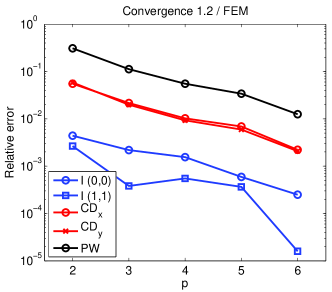
It is interesting to note that even when the differences of the investigated diffraction order intensities are only relatively small (e.g., differences only in the third significant digit) there are significant differences in the resulting aerial images and in the process windows (e.g., differences in the first or second significant digit). Figure 3 shows the convergence behavior of the FEM near field and far field results graphically.
Table 4 lists results for the case of a periodic array of contact holes with large pitch (quasi isolated case), Layout 1.3. Due to the large size of the computational domain, in this case the WGM solver is switched to the decomposition mode (see Chapter 2.1). This approach contains some approximations to the rigorous model, therefore it is expected that the results do not exactly converge to the numbers obtained with the finite element method. As can be seen from the table, the higher order near field diffraction orders converge to numbers with a few percent offset from the rigorous results. The CD’s obtained with FEM and obtained with WGM differ by about 5 nm and the process windows differ by about 20 nm.
3.2 Z-like structures
In this section we investigate structures which include 45-degree angles in the --plane. These structures are favourable from the electronic design point of view, however, they are critical for optical simulators relying on --structured meshes. Figure 4 shows a schematics of the Z-like structures. We investigate two cases for structures with minimal critical dimensions of 45 nm, resp. 65 nm (). The corresponding geometrical parameters are listed in Table 1 (Layout 2.1, 2.2).
a) \psfrag{CDx}{\tiny$\mbox{CD}_{\mbox{x}}$}\psfrag{CDy}{\small$\mbox{CD}_{\mbox{y}}$}\psfrag{px}{$\mbox{p}_{\mbox{x}}$}\psfrag{py}{$\mbox{p}_{\mbox{y}}$}\psfrag{Lx}{$\mbox{L}_{\mbox{x}}$}\psfrag{Ly}{$\mbox{L}_{\mbox{y}}$}\includegraphics[height=130.08731pt]{figures/schema_geo_z_1.eps} b) \psfrag{CDx}{\tiny$\mbox{CD}_{\mbox{x}}$}\psfrag{CDy}{\small$\mbox{CD}_{\mbox{y}}$}\psfrag{px}{$\mbox{p}_{\mbox{x}}$}\psfrag{py}{$\mbox{p}_{\mbox{y}}$}\psfrag{Lx}{$\mbox{L}_{\mbox{x}}$}\psfrag{Ly}{$\mbox{L}_{\mbox{y}}$}\includegraphics[height=130.08731pt]{figures/resist_topography.eps}
| Layout 2.1 | |||||||||
| p | t [s] | N | RAM | ||||||
| [GB] | [nm] | [nm] | [nm] | ||||||
| JCMsuite (FEM) | 2 | 6 | 33810 | 0.3 | 0.29313 | 0.07655 | 65.12 | 40.22 | 200.13 |
| 3 | 23 | 50400 | 0.7 | 0.29127 | 0.07750 | 66.07 | 38.58 | 197.27 | |
| 4 | 53 | 63700 | 1.1 | 0.29001 | 0.07652 | 60.93 | 38.18 | 174.42 | |
| 5 | 73 | 84000 | 2.0 | 0.29100 | 0.07720 | 62.57 | 39.25 | 183.98 | |
| 6 | 143 | 111720 | 3.1 | 0.29133 | 0.07743 | 63.81 | 39.00 | 188.74 | |
| 7 | 369 | 172480 | 5.9 | 0.29084 | 0.07751 | 63.75 | 38.32 | 186.88 | |
| Dr.LiTHO (WGM) | 23 | 36400 | 1.7 | 52.25 | 35.66 | 92.46 | |||
| Layout 2.2 | |||||||||
| JCMsuite (FEM) | 2 | 17 | 63798 | 0.7 | 0.05471 | 0.10008 | 82.73 | 52.88 | NaN |
| 3 | 54 | 82320 | 1.3 | 0.05544 | 0.09985 | 87.30 | 57.06 | 58.23 | |
| 4 | 172 | 127400 | 2.7 | 0.06267 | 0.09916 | 89.14 | 60.81 | 90.02 | |
| 5 | 196 | 188160 | 4.9 | 0.06583 | 0.10022 | 94.36 | 62.36 | 108.12 | |
| 6 | 227 | 156408 | 4.4 | 0.06428 | 0.10157 | 94.24 | 61.48 | 105.10 | |
| 7 | 509 | 241472 | 8.0 | 0.06302 | 0.10156 | 92.50 | 60.94 | 94.83 | |
| Dr.LiTHO (WGM) | 182 | 0.1 | 86.01 | 65.04 | 31.10 | ||||
Table 5 shows convergence results for the investigated cases of Z-like structures. Due to the larger computational domain and the more complex structure, the computational effort is larger than in the contact hole cases, Chapter 3.1. In the first case (Chromium material stack, Layout 2.1), FEM shows convergence of the CD’s with an accuracy of about 0.1-1 nm, and of the process window of about 2 nm. Computation time for the most accurate FEM result was about 5 minutes (using 8 cores of a multi-processor workstation). The full 3D waveguide method result with a trunctation number of 23 yields results with a CD difference between the methods in the 10%-range, and consequently also a large numerical difference between the process window width results. Due to the high number of Fourier modes taken into account, the computation time was several hours (using a single processor on a standard PC).
Probably due to the more involved material properties of the second example of this chapter, Layout 2.2, the convergence is less pronounced than in the first example. For FEM, CD accuracies in the range of 2 nm are reached at computation times below 10 min, and the process window width seems still not to be clearly converged to a certain region. The waveguide method (in decomposition mode) yields CD results which are different from the FEM results by about 5 nm (with different signs for - and -directions) and a process window width which is about one third of the FEM process window width.
The case of a geometry with a 45-degree angle is clearly more straight-forward for a FEM solver, because FEM does not rely on regular grids and can resolve arbitrary angles and shapes. Therefore the advantage of FEM in the comparison of the rigorous solvers (for Layout 2.1) is clear. The case is also involved for the decomposition strategy of the waveguide method, due to the mutual influence of the various decomposed regions which is partly neglected in this strategy.
Figure 4 b) shows the resist topography after etch. This resist simulation has been performed using a 80 nm resist and further undisclosed resist parameters without any optimization. This simulation result demonstrates the availability of a full lithography simulation environment for highly accurate simulations including advanced geometrical mask setups.
3.3 Larger and more complex patterned mask
a)
 b)
b)
 c)
c)
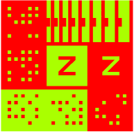
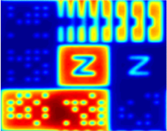
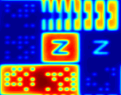
In this section we present results of simulations of a larger section of a mask. Figure 5 a) shows the layout, where red regions correspond to material and green corresponds to blank regions. The layout contains 65 nm holes and posts (1X, 260 nm in mask scale), two Z-like structures with parameters corresponding to Layout 2.2 and further test structures. Material and illumination and imaging parameters are listed in Table 2 (material stack 1).
| Layout 3 () | ||||||
|---|---|---|---|---|---|---|
| p | t [s] | N | RAM [GB] | |||
| JCMsuite (FEM) | 3 | 1490 | 1108800 | 0.6038803 | 0.0720966 | |
| 3 | 1637 | 1206000 | 30 | 0.6043494 | 0.0720739 | |
| 3 | 1967 | 1335600 | 0.6044032 | 0.0721372 | ||
| 3 | 2588 | 1617600 | 0.6043363 | 0.0719821 | ||
| 4 | 1419 | 1201200 | 0.6066360 | 0.0726171 | ||
| 4 | 1627 | 1306500 | 33 | 0.6060792 | 0.0725927 | |
| 4 | 1860 | 1446900 | 0.6056927 | 0.0724837 | ||
| 4 | 2299 | 1752400 | 47 | 0.6050683 | 0.0723238 | |
| 5 | 5037 | 2217600 | 70 | 0.6057829 | 0.0721241 | |
| 5 | 5524 | 2412000 | 76 | 0.6054997 | 0.0721632 | |
| 5 | 6182 | 2671200 | 86 | 0.6053901 | 0.0721646 | |
| 5 | 8266 | 3235200 | 108 | 0.6054001 | 0.0722620 | |
| Dr.LiTHO (WGM) | 20800 | 0.15 | 0.6067974 | 0.0717071 | ||
a)
 b)
b)
 c)
c)
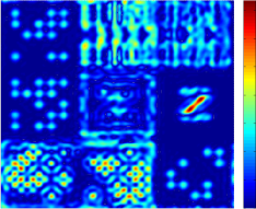
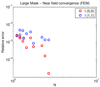
Table 6 shows the convergence of the near field results obtained with the FEM solver for different numerical parameter settings. From the data for the diffraction order intensities it can be seen that the relative error of the significant diffraction efficiencies converges well to the range of about 0.1%. Convergence with finite element degree as well as convergence with mesh refinement, resp. N, can be observed. Due to the large size of the problem we have not investigated far field convergence in detail in this case. However, the numerical settings in this case are similar to the settings in the previous chapters, i.e., we expect the accuracy also of the far field results to be of the same quality as in Sections 3.1 and 3.2 for the examples with the same material stacks. This is also supported by the apparent good convergence of the near field results. Further Table 6 shows computation time and memory consumption for WGM, for the computation yielding the result displayed in Figure 6 b). Here the domain decomposition strategy of the solver has been applied (cf. 2.1). Please note that the computational effort in computation time is comparable (JCMsuite used eight threads in parallel in this case, while Dr.LiTHO was used single-threaded) and that the computational effort in terms of memory consumption is several orders of magnitude larger for FEM.
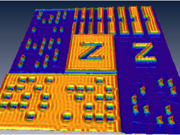
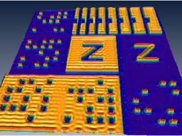
Figure 5 b,c) shows near field distributions (at the upper boundary of the mask) with source fields of different polarizations in a pseudocolor representation. Interference fringes and field singularities at metal edges and corners can be observed. Figure 6 a,b) shows corresponding aerial images, for near field computations with FEM and with WGM. The images correspond very well to each other. Plotting the differences of the fields (Figure 6 c), one observes that difference of the aerial image is not randomly distributed but localized especially around the Z features and at the 65 nm contact holes and posts. Please note the very good qualitative agreement of the aerial image computed with WGM and with FEM.
4 Conclusions
We have developed an interface between the lithography simulator Dr.LiTHO and the electromagnetic field solver JCMsuite. We have demonstrated a typical lithography simulation flow from the near field simulation to resist image formation, post-exposure bake and development. Further, FEM-based JCMsuite and a WGM-based solver from the package Dr.LiTHO have been benchmarked. Both solvers have specific advantages and resulting from that specific fields of applications. For standard lithography structures WGM is more qualified. For more complex structures and for cases where a very high accuracy is required FEM is more qualified. Therefore the combination of Dr.LiTHO and JCMsuite forms a very efficient lithography simulation environment for all fields of applications.
References
- [1] ITRS, “International technology roadmap for semiconductors,” 2007 update. http://www.itrs.net.
- [2] P. Evanschitzky, F. Shao, A. Erdmann, and D. Reibold, “Simulation of larger mask areas using the waveguide method with fast decomposition technique,” Proc. SPIE 6730, p. 67301P1, 2007.
- [3] S. Burger, R. Köhle, L. Zschiedrich, W. Gao, F. Schmidt, R. März, and C. Nölscher, “Benchmark of FEM, waveguide and FDTD algorithms for rigorous mask simulation,” in Photomask Technology, J. T. Weed and P. M. Martin, eds., 5992, pp. 378–389, Proc. SPIE, 2005.
- [4] S. Burger, R. Köhle, L. Zschiedrich, H. Nguyen, F. Schmidt, R. März, and C. Nölscher, “Rigorous simulation of 3D masks,” in Photomask Technology, P. M. Martin and R. J. Naber, eds., 6349, p. 63494Z, Proc. SPIE, 2006.
- [5] S. Burger, L. Zschiedrich, F. Schmidt, R. Köhle, B. Küchler, and C. Nölscher, “EMF simulations of isolated and periodic 3D photomask patterns,” in Photomask Technology, 6730, p. 67301W, Proc. SPIE, 2007.
- [6] P. Evanschitzky and A. Erdmann, “Fast near field simulation of optical and EUV masks using the waveguide method,” Proc. SPIE 6533, 2007.
- [7] K. D. Lucas, H. Tanabe, and A. Strojwas, “Efficient and rigorous three dimensional model for optical lithography simulation,” J. Opt. Soc. Am. A 13, p. 2187, 1996.
- [8] M. G. Moharam, D. A. Pommet, E. B. Grann, and T. K. Gaylord, “Simple implementation of the rigorous coupled-wave analysis for surface relief gratings: Enhanced transmittance matrix approach,” J. Opt. Soc. Am. A 12, p. 1077, 1995.
- [9] J. Turunen, “Form birefringence limits of Fourier expansion methods in grating theory: errata,” J. Opt. Soc. Am. A 14, p. 2313, 1997.
- [10] A. Erdmann, C. Kalus, T. Schmöller, and A. Wolter, “Efficient simulation of light diffraction from 3-dimensional EUV-masks using field decomposition techniques,” Proc. SPIE 5037, 2003.
- [11] L. Zschiedrich and F. Schmidt, “Finite element simulation of light propagation in non-periodic mask patterns,” in Photomask and Next-Generation Lithography Mask Technology XV, T. Horiuchi, ed., 7028, p. 702831, Proc. SPIE, 2008.
- [12] P. Monk, Finite Element Methods for Maxwell’s Equations, Claredon Press, Oxford, 2003.
- [13] L. Zschiedrich, S. Burger, A. Schädle, and F. Schmidt, “A rigorous finite-element domain decomposition method for electromagnetic near field simulations,” in Optical Microlithography XXI, 6924, p. 692450, Proc. SPIE, 2008.
- [14] J. Pomplun, S. Burger, L. Zschiedrich, and F. Schmidt, “Adaptive finite element method for simulation of optical nano structures,” phys. stat. sol. (b) 244, p. 3419, 2007.
- [15] T. Fühner, T. Schnattinger, G. Ardelean, and A. Erdmann, “Dr.LiTHO: a development and research lithography simulator,” Optical Microlithography XX 6520, p. 65203F, SPIE, 2007.