Strategies for optimal design for electrostatic energy storage in quantum multiwell heterostructures
Abstract
The physical principles are studied for the optimal design of a quantum multiwell heterostructure working as an electrostatic energy storage device. We performed the search for an optimal multiwell trapping potential for electrons that results in the maximum static palarizability of the system. The response of the heterostructure is modeled quantum mechanically using nonlocal linear response theory. Three main design strategies are identified, which lead to the maximization of the stored energy. We found that the efficiency of each strategy crucially depends on the temperature and the broadening of electron levels. The energy density for optimized heterostructures can exceed the nonoptimized value by a factor more than . These findings provide a basis for the development of new nanoscale capacitors with high energy density storage capabilities.
Attaining high density electromagnetic energy storage is a vital technological and scientific problem, since electricity is the most universal and scalable form of energy. In addition, the continued progress in chip design also produces demands for nanoscale capacitors with the enhanced energy density. Recently, different types of nanostructures, such as multi-walled doped carbon nanotubes nisoli or metal-dielectric interfaces interface ; nature have attracted much attention as potential building blocks for high energy density storage devices.
There is no clear understanding of the physical principles for optimal design on scales where quantum mechanical effects (e. g., like discreteness of energy levels, tunneling and nonlocality of dielectric response) start to play a significant role. A recent study NJP predicted the surprising effect that there is an optimal size for small metallic dimers resulting in maximal electromagnetic energy density between the particles. This behavior is contrary to the classical theory produces a monotonous increase of the energy density with decreasing size of a dimer. Similar simulations, but using more sophisticated ab initio techniques prl confirmed the correctness of qualitative predictions made in NJP . This confirmation provides a foundation for performing a systematic study of the principles of optimal design of nanocapacitors using the formalism developed prl2006 , thereby avoiding much more computationally expensive ab initio simulations.
The present study focuses on the static limit of the dielectric response of heterostructures. A dynamic field may result in higher energy densities due to the resonance phenomena, however, this benefit is offset by much higher losses in the dielectric, which is not acceptable for energy storage applications. In the static regime, there are still energy losses due to electron-phonon coupling, etc. Typical values for the dissipation factor (reciprocal to the quality factor) is of the order or less. In the present study we assume zero dissipation factor in the static limit.
This Letter considers a quantum multi-well heterostructure working as an electrostatic energy storage device. We assume that the heterostructure is placed between two leads, without direct contact to the leads, permitting the neglect of tunneling effects. If a constant bias is applied to the leads, the electron density in the multi-well heterostructure becomes perturbed resulting in a finite polarization of the nanostructure. The energy stored in the heterostructure depends on the dielectric function of the heterostructure, which is determined by the eigenfunctions and eigenenergies of the confined electrons. The goal of optimal design is to find a shape for the heterostructure, which maximizes the stored electrostatic energy. In the present simulations a multi-well heterostructure is modeled by the Hamiltonian , where is the electron effective trapping potential.
Since inhomogeneous systems with a few electrons can have an electromagnetic response very different from the bulk, in our simulations we use the non-local density-density response function within the coordinate-space representation :
| (1) |
where is the Fermi filling factor and the small constant describes the level broadening, and and are the eigenenergies and eigenfunctions of the Hamiltonian , and is the frequency of the external bias field. The electron eigenenergies and eigenfunctions are obtained numerically using spacial discretization of the Schrödinger equation. Eq.(Strategies for optimal design for electrostatic energy storage in quantum multiwell heterostructures) permits calculation of the induced electric field in the system within linear response theory prl2006 .
The effective trapping potential is represented as a sum of model potentials located at the positions , , which may be controlled during the material fabrication procedure: . For simplicity we assume to be the Coulomb potential of a charge with a cutoff : , for , , for . The algorithm searches for optimal parameters to maximize the stored electrostatic energy in the system , where the integration is performed over the volume of the nanostructure. The search for the optimal potential is performed using Brent’s “principal axis” optimization algorithm brent for a scalar function of several variables.
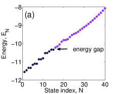
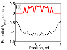
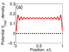
To simplify our simulations we consider a quasi-one dimensional system of length . Then is the unit of energy determined by the system, where is the electron mass. The optimization of the trapping potential is performed at the static limit of the external field , with electrons trapped in the heterostructure having wells. The cut-off parameter is chosen as , and to ensure the total neutrality of the heterostructure. Note, that in all the simulations we assume , that is equivalent . Fig.1(a) shows the eigenspectrum for a non-optimized potential, corresponding to equally spaced potential wells (Fig.1(c)). The occupied states colored in blue and unoccupied states are shown in magenta. Note, that the trapping potential is scaled down by the factor of for better visibility.
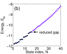
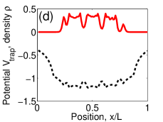
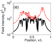
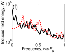
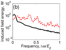
First we perform the optimization for relatively small level broadening and temperature K. The optimized heterostructure has the eigenspectrum shown in Fig.1(b), and Fig.1(d) shows the optimized trapping potential and the corresponding ground state electron density. Note, that the optimized potential has a dramatically decreased energy gap between the highest occupied and the lowest unoccupied energy levels. The initial energy gap is , and after the optimization . For the field enhancement estimate we only need the term in Eq.(Strategies for optimal design for electrostatic energy storage in quantum multiwell heterostructures) describing the transition between levels and . The decrease of the energy gap leads to an enhancement of the transition by approximately , and the corresponding field intensity (and stored energy ) by a factor of , compared to the non-optimized potential Fig.1(e). Potentially even further enhancement of the polarization may be achieved, if there are several unoccupied energy levels (i.e. a higher density of states), close to the highest occupied one.
Since the energy stored in the heterostructure is increased by approximately factor of in the static limit (see Fig.1(f)), it is clear, that the vanishing of the gap is a significant, but not the only mechanism for the field enhancement. The enhancement of the transition dipole matrix elements, including for is another mechanism. However, for narrow energy levels this mechanism gives a relatively less significant contribution of a factor of .
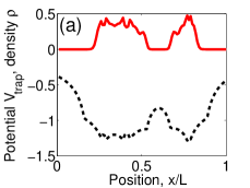
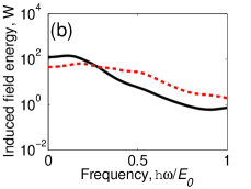
Upon increasing the level broadening the dipole mechanism becomes more significant. In Fig.2 we consider optimization of the trapping potential in a case of larger level broadening . First, for the optimized heterostructure in Fig.2(a) the electron density has the shape with two maxima, resulting in a bigger dipole response of the system. Second, for the optimized trapping potential the enhancement of the energy stored in the heterostructure Fig.2(b) is much more modest, compared to Fig.1(f). The optimized design provides improvement of the stored energy by a factor of . Third, the energy gap for the optimized potential is smaller, than in the non-optimized one (see Fig.1(a)), but it is still times larger than in Fig.1(b). Thus, the contribution due to the resonant effect and the contribution due to the enhancement of the dipole matrix elements are much closer, than in the previous example, with narrower energy levels. Note, that the optimized potential for produces significantly less polarization than the optimized potential in Fig.2(a). We conclude, that level broadening makes the previously optimized design of the heterostructure non-optimal.
We also studied the optimization of the trapping potential at K in Fig.3. Surprisingly, at the relatively high temperature (here is the Boltzmann constant), the optimization gives as the best result, corresponding to a square well potential. A reasonable explanation of this surprising result is that the square well potential gives the fastest scaling of the energy levels , producing the maximum energy gap , and as a result, the maximum population difference .
In conclusion, we have studied the principles of optimal design of heterostructures, which function as nanoscale capacitors. Three main strategies to maximize the stored electrostatic energy were identified. The first one is the minimization of the energy gap , the second is the maximization of the transition dipole matrix elements for the electrons in the heterostructure, and the third is the maximization of the population difference in the system. The effectiveness of each strategy depends the level broadening and temperature of the system, which we treated as independent parameters. Note, that the first and the third strategies are mutually exclusive.
Some caution is necessary, as the minimization the energy gap between the highest occupied and lowest unoccupied levels is equivalent to making system “more metallic”. In this case the conductivity in such system should grow in the same way as the susceptibility as a function of the energy gap , which is consistent with experimental findings interface . Since for energy storage applications one needs nanocapacitors with relatively small inner charge leakage, the scaling of the electrical conductivity and tunneling effects have to be taken into account. Another effect, which we can not take into account within linear response theory is the dielectric breakdown. The increase of the breakdown voltage is favorable for energy storage applications, since the electrostatic stored energy , where the maximum work voltage cannot exceed the breakdown limit. In general, smaller energy gap will result in a smaller critical breakdown voltage for bulk materials, however, for spatially inhomogeneous nanostructures more systematic ab initio simulations are desirable.
References
- (1) G. Chen et al. Phys. Rev. Lett 90, 257403 (2003).
- (2) S. K. Saha, M. DaSilva, Q.Hang, T. Sands and D.B. Janes, Nanotechnology, 17, 2284 (2006).
- (3) P. Banerjee, I. Perez, L. Henn-Lecordier, S. B. Lee, G. W. Rubloff, Nature Nanotechnology, 4, 292 (2009).
- (4) I. Grigorenko, A. Balatsky, S. Haas, A. F. J. Levi, New J. of Phys., 10, 043017 (2008).
- (5) K. Zhao, et al. Phys. Rev. Lett 102, 186804 (2009).
- (6) I. Grigorenko, S. Haas, A. F. J. Levi, Phys. Rev. Lett. 97, 036806 (2006).
- (7) R.P. Brent, Algorithms for minimization without derivatives, Mineola, New York, Dover, 2002; K. R. Gegenfurtner, Behav. Res. Meth. Instrum. Comput., 24, 560 (1992).