Current-induced interactions of multiple domain walls in magnetic quantum wires
Abstract
We show that an applied charge current in a magnetic nanowire containing domain walls (DWs) results in an interaction between DWs mediated by spin-dependent interferences of the scattered carriers. The energy and torque associated with this interaction show an oscillatory behaviour as a function of the mutual DWs orientations and separations, thus affecting the DWs’ arrangements and shapes. Based on the derived DWs interaction energy and torque we calculate DW dynamics and uncover potential applications of interacting DWs as a tunable nano-mechanical oscillator. We also discuss the effect of impurities on the DW interaction.
pacs:
75.60.Ch,75.75.+a,75.60.JkI Introduction
Domain walls (DWs), i.e. regions of noncollinearity separating areas of different homogenous magnetization directions, are important from a fundamental and application point of view Yamanouchi et al. (2004); Yamaguchi et al. (2004); Parkin et al. (2008). This is particularly the case at low dimensions, as in magnetic nanowires carriers turn out to couple strongly with DWs Klaeui (2008) leading to a marked influence on the wire’s transport properties, e.g. DW magnetoresistances in the range of 1000% were reported Ebels et al. (2000); Chopra and Hua (2002); Rüster et al. (2003) . As this coupling is associated with a change of the carriers’ spin, it results in a current-induced spin torque acting on the DW and consequently in a current-induced DW motion Yamanouchi et al. (2004); Yamaguchi et al. (2004). Based on these facts magnetic nanowires with a series of DWs can be utilized as a “racetrack DW memory” Parkin et al. (2008). The DWs’ motion is current-controlled; DWs separated by rather small distances are addressable thus allowing for a high memory density.
In another context it is established that strong carrier scattering and interference results in long-range interactions between impurities on metal surfaces. This interaction governs the impurities geometric arrangements and growth Lau and Kohn (1978); Bogicevic et al. (2000); Fichthorn and Scheffler (2000); Silly et al. (2004); Knorr et al. (2002); Stepanyuk et al. (2004). The question of whether and how the carriers’ spin dependent scattering mediates interactions between DWs is still outstanding and should be addressed here. Clearly, the answer is of vital importance for a high-density nanowire-based racetrack memory and adds a new twist on interference-mediated interactions. We focus on the current-induced part of the coupling between neighboring DWs in a magnetic nanowire. Based on our results we identify the following mechanism of the DWs coupling: Upon scattering from the first DW a carrier spiral spin density builds up. This acts as a spatially non-uniform torque on the second DW whose energetically stable shape and position show therefore a non-uniform dependence on the distance from the first DW. This is different from the spin-torque transfer in bulk spin valve systems Slonczewski (1996); Berger (1996); Barnaś et al. (2005) or magnetic tunnel junctions Slonczewski (1989); Theodonis et al. (2006) insofar as in our case the DWs spatial arrangement, in addition to the magnetization direction, is current controlled 111Also note, in reduced dimensions, e.g. a constrained nanowires, the propagation of the transverse component of the torque is strongly enhanced; in contrast this component is suppressed in bulk systems Stiles and Zangwill (2002).. We develop a theoretical framework to calculate the DWs current-induced effective potential and find it oscillates with the distance of DWs and their mutual polarization directions. This interaction we employ to study the DWs dynamics. As an application we propose the use of this new effect as a tunable, current-driven two-DW magnetic nano-oscillator Katine et al. (2000); Kiselev et al. (2003); Kaka et al. (2005); with a radiation emission dependent on the DWs positions in the various possible stable configurations.
II Theoretical model
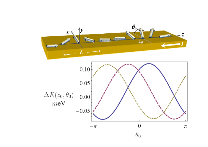
We consider a magnetic nanowire with two DWs when an electric current is transmitted through the wire (a schematic is shown in Fig. 1). When the distance between DWs is larger than the phase coherence length , DWs act as independent scatterers. For the current transmission mediates DW coupling. For definiteness, we assume that one of the DWs (located at ) is pinned, e.g. by a geometric constriction, and concentrate on the effect of the current on the second DW, initially (i.e., for ) located at . For each DW has an extension . The transverse dimensions of the wire should be smaller than the exchange length and the Fermi wave length of the carriers, a situation realizable for magnetic semiconductors. The Hamiltonian of independent carriers coupled (with a coupling constant ) to a spatially non-uniform magnetization (DWs) profile is modeled by (we use units with )
| (1) |
where and are the creation and annihilation operators of electrons with spin . Applying a local gauge transformation Korenman et al. (1977); Tatara and Fukuyama (1997); Dugaev et al. (2002) we obtain instead of the nonuniform magnetization a Zeeman splitting term and a spin-dependent spatially varying potential , which for can be treated perturbatively Korenman et al. (1977); Tatara and Fukuyama (1997); Dugaev et al. (2002, 2007) ( is the Fermi wave vector). Note, for a sharp domain wall, i.e. for , the formalism of Ref.Dugaev et al. (2003a) can be adopted. is obtained from the requirement , where is the unit vector along , . The transformed Hamiltonian reads
| (2) |
with the perturbation given by
| (3) |
and is a gauge potential. For a wire with two DWs we parametrize the magnetization profile by the angles and (cf. Fig.1)
| (4) | |||||
| (5) |
(See reference Thiavill and Nakatani (2006) and references therein.) The angle describes the relative orientation between the wall pinned at and the other situated around . We set to zero at the first wall and around the second (see Fig. 1 ). For the walls are antialigned. For DWs may merge, hence we consider the case for which we may write , where ()
| (6) | |||||
This approach is generalizable to any number of DWs, which are sufficiently far apart. As shown in Refs.Tatara and Fukuyama (1997); Dugaev et al. (2002, 2007) for a single DW, for , i.e. when hardly varies within (adiabatic DW), the terms in Eq. (6) proportional to are negligibly small and a perturbative approach is appropriate for treating the electron scattering from the DWs potential (Eq. (6)) 222In fact, as shown in Dugaev et al. (2007), this approach is justifiable even for Dugaev et al. (2007).. Assuming to be the wave function of an independent electron with energy in the wire without the DWs, we find the first-order correction due to the perturbation , i.e. due to scattering from the first DWs, as
| (7) |
The Green’s function corresponds to the unperturbed Hamiltonian with . It is diagonal in spin space with elements
| (8) |
where for lifetimes , and . Hence
| (9) |
and
| (10) |
for incoming electrons of spin up and down, respectively.
The interaction energy of the two DWs due to the single scattered state is calculated as
| (11) |
Summing up the contributions of all scattering states in the energy range between and , for an applied voltage , we obtain the current-induced coupling of the DWs as
| (12) |
where is the velocity of electrons at the Fermi level.
III Numerical examples
Magnetic semiconductors Rüster et al. (2003); Sugawara et al. (2008) are most favorable for a sizable effect, for metallic wires the 1D limit is also within reach Schäfer et al. (2008). Here we use in the numerical calculations similar parameters as in Ref.Rüster et al., 2003, i.e. nm; a mean free path of nm; an effective mass of ( is free electron mass); ; meV; meV; and . 333We note that the conditions for our theory to be applicable is that the mean free path should be larger than the distance between the DWs. A carrier wave length larger than means a complete localization (Ioffe-Regel criteria of localization), a case which is not of interest here. On the other hand, in a magnetic semiconductor, can be enhanced by lowering the acceptors density (and/or ordering them). The width of the wall may well be on the atomic size in the presence of constrictionsBruno (1999); Pietzsch et al. (2000); Ebels et al. (2000), i.e. well below the DW lengths in bulk materials. In such a situation, the DW-interaction increases due to the strongly enhanced DW scattering Araújo et al. (2006); Dugaev et al. (2006a, b, 2005). The interaction energy Figure 1 depends periodically on the DWs mutual angle and distance , which results in an oscillating motion of the DW along the axis as well as an oscillating direction of DW polarization.
Now we focus on the effect of DW scattering on the electron spin density, leading to a nonequilibrium spin accumulation and to a spin torque acting on the wall. Subsequently, we study the dynamics of the DW related to the DW coupling.
The spin-density due to the single transmitted wave of spin is
| (13) |
and the total current-induced spin density is Dugaev et al. (2003b)
| (14) |
We find that the correction to the spin density follows the magnetization profile with additional Friedel oscillations, which are a superposition of two waves with periods and . The oscillations in the spin density are smaller in magnitude than the overall spin density profile and decay with increasing .
We calculate the current-induced torque acting on the second DW at from
| (15) |
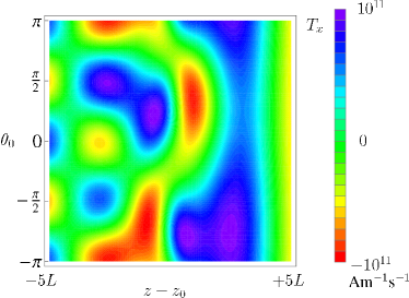
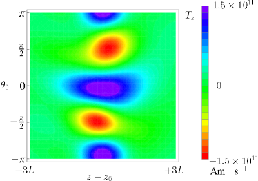
where , is the Landé factor and is the Bohr magneton. We assumed a thin nanowire with a cross section of nm2 as in Ref. Rüster et al. (2003). In Eq. (15) is the correction to the electron spin density due to scattering. The calculated torque on the second DW is shown in Figs. 2 and 3, where and Am-1 were usedSugawara et al. (2008). The correction to the spin torque shows that the force upon the DW depends strongly on their relative polarizations.
To inspect the current-induced dynamics of the DW at , we evaluate the accumulated spin density that acts on the DW at . The DW magnetization dynamics are then modeled using the Landau-Lifshitz equation 444The inclusion of Gilbert damping is straightforward and has only a minor effect for the case of weak damping.
| (16) |
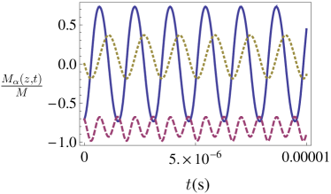
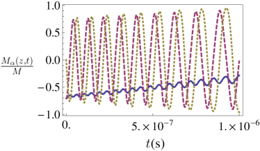
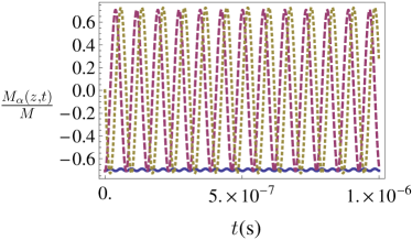
As an initial condition we assume that the magnetization profile in the wire without electric current is described by Eq. (5). The results for the time dependence of the magnetization are shown in Fig. 4 for the centre of the DW, . We should note that the relative orientation of the walls at the start of motion does play a role in the type of motion we see. Here we present it for an arbitrary configuration. As we move away from the centre of the DW, the relative orientation becomes increasingly irrelevant. At the motion is the same regardless of the value of .
Analyzing different magnetization components, we find their motions have different frequencies and a different form. No lateral movement or permanent distortion of the DW is observed, we see only oscillations. At the edge of the DW wall there are small rotations of the magnetization, regardless of the initial conditions. If we move far from the DW then all the dynamics of the magnetization vanish.
This is in contrast to the case where we do not include the first domain wall. In this case there is no motion near the centre of the domain wall at all. Furthermore the oscillations in the magnetization towards the edge of the domain wall are much slower (by several orders of magnitude) than exhibited here.
Extending our analysis to include the effect of magnetic anisotropy we write
| (17) |
We take the anisotropy constant , and therefore the -axis as a hard magnetization axis. Figure 5 shows the effects of anisotropy on the domain wall motion. The anisotropy dampens motion in the x-direction, thus exacerbating the y and z oscillations. This is also in contrast to the case where we ignore the first domain wall. In this case, although the anisotropy does introduce motion around the centre of the domain wall it does not involve a decaying -component, see Fig. 6.
IV Summary
A current through a magnetic nanowire containing DWs results in a DW interaction mediated by the scattered charge carriers. We developed a method for calculating the interaction energy and the consequences of this new coupling mechanism. The DWs interaction energy oscillates as a function of the DWs mutual orientation and distance. This has immediate consequences on how DWs rearrange upon applying a bias voltage and on the fundamental limit of the DWs packing density. In fact, different parts of the DW oscillate at different rates and in different ways: becoming more regular, smaller, and quicker away from the DW centre. The nonequilibrium DWs oscillations around the energy minima generates radiation with a frequency dependent on the applied bias voltage, DW length and scattering strength. These parameters are externally tunable for utilizing the interacting DWs as a versatile radiation source. For an experimental realization magnetic semiconductors Ohno (1998); Sugawara et al. (2008); Rüster et al. (2003); Koike et al. (2005); Fukumara et al. (2005); Holleitner et al. (2005) are favorable, our results are in the range already achievable Rüster et al. (2003). Extension to the metallic case is straightforward, though DW lengths may not be easily fabricated on the required scale. In this case the results remain qualitatively similar. Furthermore anisotropy will completely dampen any DW oscillations as motion in a plane becomes much harder due to the much larger magnetization size, Am-1 for Fe.
In our numerical simulations we used parameters of a magnetic semiconductor with relatively large electron wavelength, , and much longer mean free path . The latter can be realized in case of small density of impurities and defects. However, magnetic semiconductors like GaMnAs are usually strongly disordered, and instead of a strong inequality one may find . In this case, the phase of the current-induced spin density wave at a distance will be affected by impurities, and, therefore, one can expect that the disorder-averaged interaction between two DWs at a distance is suppressed by the factor . However, we should stress that the real interaction between two DWs depends only on a given realization of the disorder and therefore is not damped by the impurities. This effect is analogous to the nondamping of the RKKY interaction between magnetic impurities in disordered metalsZyuzin and Spivak (1986); Bulaevskii and Panyukov (1986). The detailed analysis of this phenomenon is beyond the scope of this paper.
Acknowledgments
This work is supported by DFG under SPP 1165, the FCT under PTDC/FIS/70843/2006 in Portugal, and by the Polish MNiSW as a research project in years 2007 – 2010.
References
- Yamanouchi et al. (2004) M. Yamanouchi, D. Chiba, F. Matsukura, and H. Ohno, Nature 428, 539 (2004).
- Yamaguchi et al. (2004) A. Yamaguchi, T. Ono, S. Nasu, K. Miyake, K. Mibu, and T. Shinjo, Phys. Rev. Lett. 92, 077205 (2004).
- Parkin et al. (2008) S. Parkin, M. Hayashi, and L. Thomas, Science 320, 190 (2008).
- Klaeui (2008) M. Klaeui, J. Phys. Condens. Matter 20, 313001 (2008).
- Ebels et al. (2000) U. Ebels, A. Radulescu, Y. Henry, L. Piraux, , and K. Ounadjela, Phys. Rev. Lett. 84, 983 (2000).
- Chopra and Hua (2002) H. Chopra and S. Hua, Phys. Rev. B 66, 020403 (2002).
- Rüster et al. (2003) C. Rüster, T. Borzenko, C. Gould, G. Schmidt, L. Molenkamp, X. Liu, T. Wojtowicz, J. Furdyna, Z. Yu, and M. Flatté, Phys. Rev. Lett. 91, 216602 (2003).
- Lau and Kohn (1978) K. Lau and W. Kohn, Surf. Sci. 75, 69 (1978).
- Bogicevic et al. (2000) A. Bogicevic, S. Ovesson, P. Hyldgaard, B. Lundqvist, H. Brune, and D. Jennison, Phys. Rev. Lett. 85, 1910 (2000).
- Fichthorn and Scheffler (2000) K. Fichthorn and M. Scheffler, Phys. Rev. Lett. 84, 5371 (2000).
- Silly et al. (2004) F. Silly, M. Pivetta, M. Ternes, F. Patthey, J. Pelz, and W. Schneider, Phys. Rev. Lett. 92, 016101 (2004).
- Knorr et al. (2002) N. Knorr, H. Brune, M. Epple, A. Hirstein, M. Schneider, and K. Kern, Phys. Rev. B 65, 115420 (2002).
- Stepanyuk et al. (2004) V. Stepanyuk, L. Niebergall, R. Longo, W. Hergert, and P. Bruno, Phys. Rev. B 70, 075414 (2004).
- Slonczewski (1996) J. Slonczewski, J. Magn. Magn. Mater. L1, 159 (1996).
- Berger (1996) L. Berger, Phys. Rev. B 54, 9353 (1996).
- Barnaś et al. (2005) J. Barnaś, A. Fert, M. Gmitra, I. Weymann, and V. Dugaev, Phys. Rev. B 72, 024426 (2005).
- Slonczewski (1989) J. Slonczewski, Phys. Rev. B 39, 6995 (1989).
- Theodonis et al. (2006) I. Theodonis, N. Kioussis, A. Kalitsov, M. Chshiev, and W. Butler, Phys. Rev. Lett. 97, 237205 (2006).
- Katine et al. (2000) J. Katine, F. Albert, R. Buhrman, E. Myers, and D. Ralph, Phys. Rev. Lett. 84, 3149 (2000).
- Kiselev et al. (2003) S. Kiselev, J. Sankey, I. Krivorotova, N. Emley, R. Schoelkopf, R. Buhrman, and D. Ralph, Nature 425, 380 (2003).
- Kaka et al. (2005) S. Kaka, M. Pufall, W. Rippard, T. Silva, S. Russek, and J. Katine, Nature 437, 389 (2005).
- Korenman et al. (1977) V. Korenman, J. Murray, and R. Prange, PRB 16, 4032 (1977).
- Tatara and Fukuyama (1997) G. Tatara and H. Fukuyama, PRL 78, 3773 (1997).
- Dugaev et al. (2002) V. Dugaev, J. Barnaś, A. Łusakowski, and L. Turski, Phys. Rev. B 65, 224419 (2002).
- Dugaev et al. (2007) V. Dugaev, V. Vieira, P. Sacramento, J. Barnaś, M. Araújo, and J. Berakdar, Int. J. Mod. Phys. 21, 1659 (2007).
- Dugaev et al. (2003a) V. Dugaev, J. Berakdar, and J. Barnaś, Phys. Rev. B 86, 104434 (2003a).
- Thiavill and Nakatani (2006) A. Thiavill and Y. Nakatani, Spin Dynamics in Confined Magnetic Structures III, Topics in Appl. Physics, vol. 101 (Springer-Verlag, Berlin, 2006).
- Sugawara et al. (2008) A. Sugawara, H. Kasai, A. Tonomura, P. Brown, R. Campion, K. Edmonds, B. Gallagher, J. Zeman, and T. Jungwirth, Phys. Rev. Lett. 100, 0477202 (2008).
- Schäfer et al. (2008) J. Schäfer, C. Blumenstein, S. Meyer, M. Wisniewski, and R. Claessen, Phys. Rev. Lett. 101, 236802 (2008).
- Bruno (1999) P. Bruno, Phys. Rev. Lett. 83, 2425 (1999).
- Pietzsch et al. (2000) O. Pietzsch, A. Kubetzka, M. Bode, and R. Wiesendanger, Phys. Rev. Lett. 84, 5212 (2000).
- Araújo et al. (2006) M. Araújo, V. Dugaev, V. Vieira, J. Berakdar, and J. Barnaś, Phys. Rev. B 74, 224429 (2006).
- Dugaev et al. (2006a) V. Dugaev, V. Vieira, P. Sacramento, J. Barnaś, M. Araújo, and J. Berakdar, Phys. Rev. B 74, 054403 (2006a).
- Dugaev et al. (2006b) V. Dugaev, J. Berakdar, and J. Barnaś, Phys. Rev. Lett. 96, 047208 (2006b).
- Dugaev et al. (2005) V. Dugaev, J. Barnaś, and J. Berakdar, Phys. Rev. B 71, 024430 (2005).
- Dugaev et al. (2003b) V. Dugaev, J. Barnaś, and J. Berakdar, J. Phys. A 36, 9263 (2003b).
- Ohno (1998) H. Ohno, Science 281, 951 (1998).
- Koike et al. (2005) T. Koike, , K. Hamaya, N. Funakoshi, Y. Takemura, Y. Kitamoto, and H. Munekata, IEEE Transactions on Magnetics 41, 2742 (2005).
- Fukumara et al. (2005) T. Fukumara, H. Toyosaki, and Y. Yamada, Semiconductor Science and Technology 20, 103 (2005).
- Holleitner et al. (2005) A. Holleitner, H. Knotz, R. Myers, A. Gossard, and D. Awschalom, Journal of Applied Physics 97, 10D314 (2005).
- Zyuzin and Spivak (1986) A. Y. Zyuzin and B. Z. Spivak, JETP Letters 43, 234 (1986).
- Bulaevskii and Panyukov (1986) L. N. Bulaevskii and S. V. Panyukov, JETP Letters 43, 240 (1986).
- Stiles and Zangwill (2002) M. Stiles and A. Zangwill, Phys. Rev. B 66, 014407 (2002).