Double-gated graphene-based devices
Abstract
We discuss transport through double gated single and few layer graphene devices. This kind of device configuration has been used to investigate the modulation of the energy band structure through the application of an external perpendicular electric field, a unique property of few layer graphene systems. Here we discuss technological details that are important for the fabrication of top gated structures, based on electron-gun evaporation of SiO2. We perform a statistical study that demonstrates how –contrary to expectations– the breakdown field of electron-gun evaporated thin SiO2 films is comparable to that of thermally grown oxide layers. We find that a high breakdown field can be achieved in evaporated SiO2 only if the oxide deposition is directly followed by the metallization of the top electrodes, without exposure to air of the SiO2 layer.
1 Introduction
The ability to isolate and embed single- and multi-layer graphene
in double gated structures is paving the way to reveal unique
electronic properties of these systems
[1, 2, 3, 4, 5, 6, 7, 8, 9, 10, 11, 12, 13].
The ability to change the voltages applied to a nano-fabricated top
gate and to the back-gate offers the possibility to gain local
control of the charge density and of imposing locally a
perpendicular electric field. This device configuration was used
recently to show how the band structure of graphene-based materials
can be tuned continuously [8, 12]. In particular,
bilayer graphene exhibits an electric field induced insulating state
due to the opening of a gap between valence and conduction band
[8], and in trilayers, which are semi-metals, the band-overlap can be increased
substantially [12]. Cleverly designed top gates on a
graphene single layer have also been used successfully for
engineering p-n junctions
[1, 2, 3, 5, 6, 7],
necessary for the investigation of Klein tunneling
[1, 3, 4], and to attempt the
fabrication of controlled quantum dots [15, 16]. Key to the
fabrication of top gated structures is the ability to deposit good
quality thin gate oxides, with high breakdown field and low
leakage current.
Here, after reviewing the relevance of double gated devices on the
electric field modulation of the band structure of double and triple
layer graphene, we discuss in some details technological aspects
related to the properties of the SiO2 layers used as gate
insulators. In particular, we discuss how we can routinely achieve
high breakdown fields in electron-gun evaporated thin SiO2 films
(15 nm), comparable to the breakdown fields of thermally grown
SiO2, which is surprising given that SiO2 deposited by
evaporation was long believed to be a poor quality insulator. To
unveil the reasons behind the good insulating quality of our
evaporated SiO2 films, we conducted a statistical study of
leakage current and breakdown voltage in capacitors, where two
metallic electrodes are separated by a SiO2 layer fabricated in
different ways. We demonstrate that if SiO2 and top gate metal
electrodes are deposited subsequently without exposing the SiO2
to air, the electrical performance of electron-gun evaporated
SiO2 is comparable to that of thermally grown SiO2. In
contrast, exposure to air of the SiO2 layer before deposition of
the counter-electrode leads to much worse insulating
characteristics. Our findings indicate that extrinsic degradation
–probably due to the absorption of humidity- has limited in the
past the insulating quality of electron-gun evaporated SiO2.
2 Device and fabrication
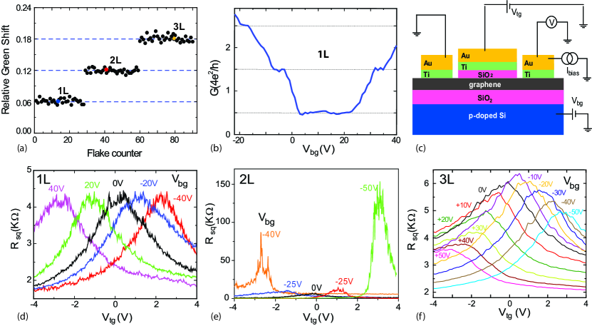
Single and few layer graphene flakes used for the device
fabrication were obtained by micro-mechanical cleavage of natural
graphite crystals, and by their subsequent transfer onto a highly
doped Silicon substrate (acting as a gate) covered by a nm
thick thermally grown SiO2 layer. The thickness of the graphene
layers can be simply identified by analyzing the shift in
intensity in the RGB green channel relative to the substrate (i.e.
Relative Green Shift)
[8, 12, 14, 17, 18].
A plot of the relative green shift, as extracted from optical
microscope images of various samples taken with a digital camera,
exhibits plateaus corresponding to the discrete thickness values -see Fig. 1a. Subsequent
transport measurements (quantum Hall effect, resistance dependence
on a perpendicular electric field, etc.) confirm the validity of
this optical method (Fig. 1b).
The fabrication of nanostructures is accomplished by conventional
electron-beam lithography. Metallic contacts and top gates were
deposited by electron-gun evaporation, respectively of Ti/Au
(nm thick with a back ground pressure of torr) for
contacts and SiO2/Ti/Au (nm thick with a back ground
pressure of torr) for top gates, followed by lift-off.
We took special care to fabricate all the ohmic contacts within 60
nm from the edges of the top gated areas, so that two probe
resistance measurements are dominated by the resistance of the
double gated region[19]. All transport measurements in
double gated devices (see Fig. 1c) were made using a
lock-in technique (excitation frequency: Hz), in the linear
transport
regime, at temperatures ranging from 300 mK up to 150K.
To understand why, contrary to expectations, we manage to achieve
high breakdown field in thin, electron-beam evaporated SiO2
films, we conducted a macroscopic study of the breakdown characteristics on two types of
capacitor test structures. The first -which we refer to as
type A- is characterized by subsequent evaporation of
SiO2/Ti/Au without breaking the vacuum in between the deposition
of the different materials. For the second -type B
SiO2- we exposed the device to ambient for one hour after the
SiO2 deposition, before evaporating the Ti/Au counter electrode.
The breakdown test measurements were made with a Keithley-2400
source-meter on more than 130 different capacitors (with three
different surface areas: , and ).
3 Transport experiments in double gated few layer graphene devices
The measurement configuration used for double gated devices is shown
in Fig. 1c. A finite voltage applied to either one of
the gates (back or top gate) changes the position of the Fermi level
in the corresponding gated region of the graphene layer, by an
amount corresponding to the induced charge density. In addition, by
biasing the two gate electrodes with opposite polarity, a large
external electric field applied perpendicular to the layer is
generated, which is equal to
( is the total SiO2 thickness). In this device
configuration, we can monitor the evolution of the in plane
transport properties for each
few layer graphene device as a function of .
Fig. 1d, e and f show the typical behavior of the
square resistance measured respectively in double gated single (d),
double (e) and triple (f) layer graphene, when sweeping the top gate,
while keeping the back gate at a fixed potential. It is apparent that
the overall electric field dependence of is markedly distinct
for graphene layers of different thickness. In all cases, the resistance exhibits a maximum
() whose value and position in gate voltage depend on
the voltage applied to the gate on which a fixed potential is
applied during the measurement. At V/m we find that for
single and bilayer graphene , close to
a conductance per square of , as expected, indicating that
the fabrication of top gate structures does not damage significantly
the material (for trilayers the square resistance is somewhat lower,
owing to the presence of an overlap between valence and conduction
band). Increasing the external electric field induces a well defined
-and different- response for the square resistance of layers of different
thickness. Respectively, in a single layer
is not affected by a finite ; in bilayers at low temperature
increases from to very large values ( K); in trilayers decreases with increasing
. These experimental findings, confirmed in a number of
different samples (3 single layers, over 10 double and 10 triple
layers) provide a clear indication that each few layer graphene is a
unique material system, with distinct electronic properties.
Transport measurements over a wide range of temperatures (from
up to ) underline the unique electronic properties of
these few layer graphene devices. In bilayer graphene the larger
, the more pronounced is the temperature dependence of
, see Fig. 2a and b. At V/m,
is only weakly temperature dependent (as it is
typical of zero-gap semiconductors), and at V/m the
observed behavior is the one typical of an insulating state. On the
contrary, trilayer graphene devices display a decrease of
when lowering the temperature, stemming for the
semimetallic nature of the constituent material.
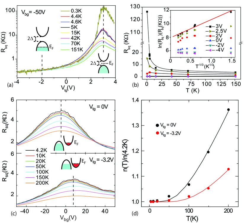
At a more quantitative level we find that in bilayer
graphene is well described by , with
K at the maximum applied external electric field
(see inset in Fig. 2b). This temperature dependence
is indicative of variable-range hopping in a two dimensional
material where an energy gap has opened, and where disorder causes
the presence of sub-gap states ( is related to this subgap density of states[8])
-making it difficult to estimate from transport experiments.
Indeed, in a disorder free bilayer graphene, at
a gap () opens in the band structure and
the density of states in the gapped region is zero. In this ideal
case, when the Fermi level is in the middle of the gapped region the value of
at a finite temperature is
entirely determined by thermally activated charge carriers ().
Therefore, can be accurately determined from a plot of
versus . On the other hand, in real devices the presence of
disorder creates a finite density of states in the the band gap of bilayer
graphene. Now charge carriers can conduct via variable-range hopping at . In this case
is a
function of the density of states at the Fermi level and not any more simply a function of .
The fact that a gap opens in the band structure of bilayer graphene at
finite is evident from the
temperature dependence of as a function of charge density.
In particular, when the Fermi level lays deep into the conduction and/or valence
band, a temperature independent is expected.
However, when the Fermi level is shifted across the energy gap region
should display an insulating temperature dependent behavior. Experimentally
this is achieved by measuring at a fixed value of
either of the gates (e.g. ) and for different voltage
applied on the other gate (e.g. ) (see Fig 2a and b). The cross over from band transport
to variable hopping range in the gap occurs at the edge of the valence and conduction band (see Fig. 2b).
Similar previous transport experiments in double gated bilayer [8]
reported an energy scale of 1-10mV associated with the insulating state induced by .
This energy scale seen in transport
is much smaller than the energy gap recently probed in optical spectroscopy experiments
( at [22]). Possibly the finite sub-gap density of states
induced by the disorder is at the origin
of the small energy scale measured in transport experiments,
however the specific mechanism responsible for these experimental observations remains an open question.
The temperature dependence of the resistance in trilayer graphene is
opposite to the one observed in bilayers, and it reveals that this
material system is a semimetal with a finite overlap () between conduction and valence band. This band overlap
can be estimated within a two band model
[12, 20, 21], where the number of thermally
excited carriers increases with temperature according to (
effective mass and equal to twice the layer spacing).
Measurements at finite show that
decreases when increasing external electric field ( goes from 32 meV to
52 meV in the measurements of Fig. 2d).
These experiments demonstrate that a perpendicular electric field
applied on few layer graphene is a valuable tool to change the band
structure of these materials. Double gated structures lead to the
discovery of the only known electric field tunable insulator, i.e.
bilayer graphene, and of the only known electric field tunable
semimetal, i.e. trilayer graphene.
4 Evaporated Silicon oxide as top gate dielectric
The opening of a sizeable band gap in bilayer graphene, and large changes in the band
overlap of graphene trilayers require the application of large external electric fields
to these material systems. It is the breakdown field of the gate-dielectric that imposes a
limit to the maximum value of experimentally accessible in double gated structures. To
optimize this aspect of the devices, we conducted a systematic study
of the breakdown electric field of SiO2 gate oxide for devices
with different areas, fabricated under different conditions. Here
we discuss the details of this investigation. From our statistical analysis
we conclude that what is crucial is not the SiO2 deposition
method, but the details in the metallization of top gate electrodes
afterwards, which affect the final quality of the oxide gate dielectric.
We compare capacitor devices fabricated following two different
procedures for one of the oxide dielectric/metal electrode
interfaces. In particular, the devices were
fabricated on a Si/SiO2 substrate (identical to the one used for
the graphene devices previously described) on which we deposit a
Ti/Au (5/20 nm) film -common electrode for the
capacitors. In devices of type A, the SiO2 deposition
and top electrode (Ti/Au 5/20 nm) metallization processes were
carried without breaking the vacuum. On the contrary in devices of
type B, the SiO2 gate dielectric was exposed to air
for one hour prior to the deposition of the top electrode metals. The SiO2 deposition
was carried out typically at torr back ground pressures. We did not observe
a dependence of the insultating properties of the SiO2 dielectric,
breakdown field and leakage current over the background pressure range from to torr.
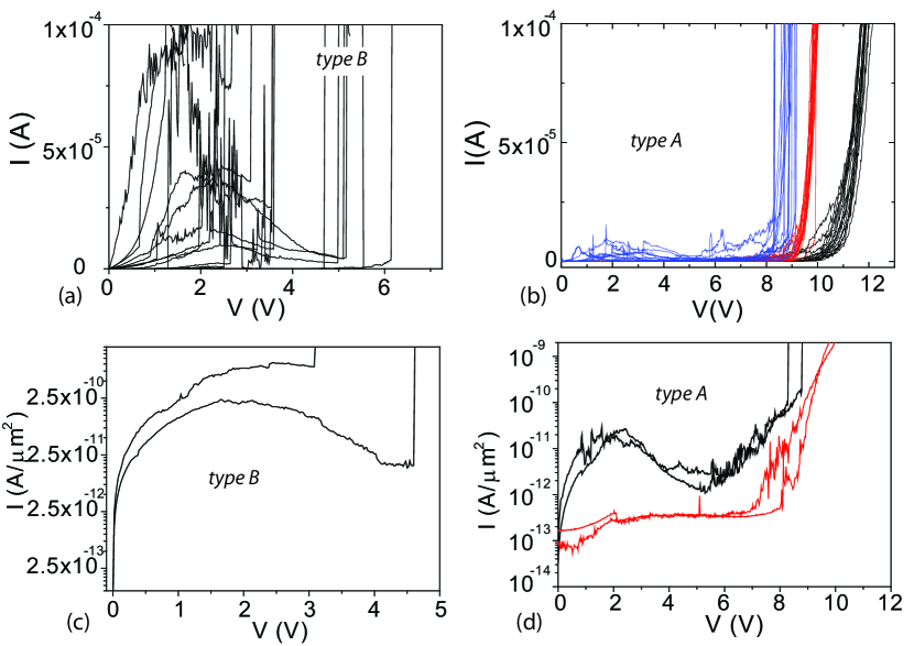
Fig. 3a and b show various traces, measured in
ambient condition, for type A and type B devices.
A first clear difference between the two types of devices is the
magnitude of the leakage current, visible by plotting the
curves both in linear and logarithmic scale, see Fig.
3. For a surface area of , we
find for the best
type B devices which is one order of magnitude larger
than that measured in the worst type A devices (the
difference for typical devices are much larger than one order of
magnitude). This extremely different level of leakage current
already indicates that the exposure of SiO2 to air previous to
the deposition of top metals has a large negative influence on the
insulating performance
of the oxide.
The characteristics further show that for a fixed surface area
(), the breakdown voltage for
type A is typically in the range whereas
type B devices breakdown anywhere in the range
. The differences in the failure of device types are
best summarized in the histogram plots of -see Fig.
4a. For type B we find a large spread
in the distribution of , in contrast to the narrow
distribution characteristic of type A devices.
Furthermore, the comparison of for type A
devices with different surface areas shows that increases
slightly with decreasing the device area, possibly indicating that
the properties of SiO2 in type A close to breakdown
are determined by small defects present in the film with rather
small probability. However, we cannot rule out that the differences
between the different sample populations originate from small
differences (2-3 nm) in the thickness of the SiO2 layers. Note,
in fact, that the leakage currents of these devices at low bias
have only small sample-to-sample fluctuations, suggesting that the
SiO2 layers in type A devices are very
uniform.
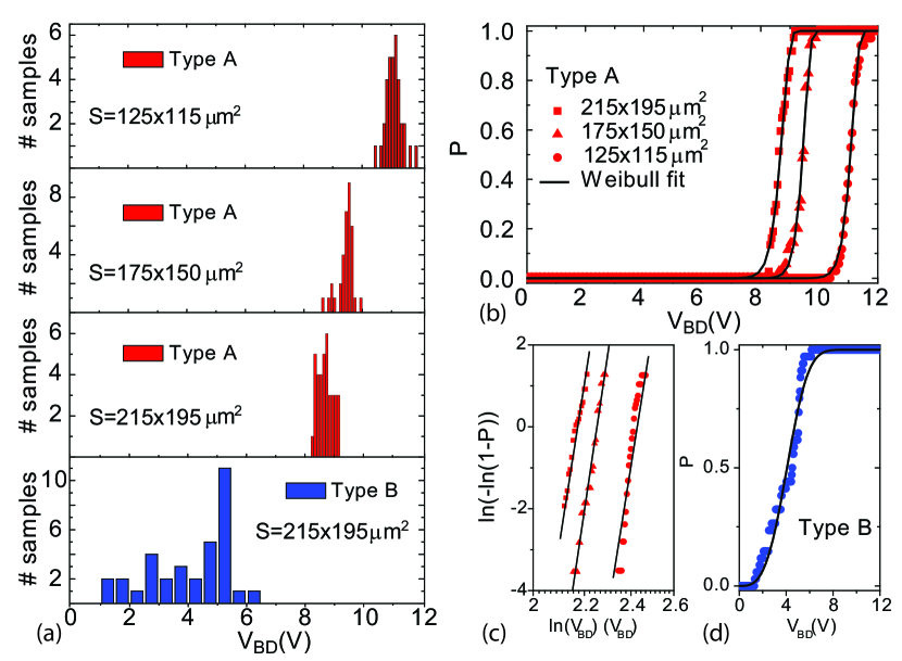
To try to quantify better our observations and analyze the role
played by the specific fabrication technique and surface areas on
the device performance (e.g. breakdown field), we adopt a failure
analysis methodology [24]. In what follows we provide a
statistical description of the breakdown probability introducing the
cumulative probability (P) as the probability of a device to
breakdown at a given voltage. From failure methodology, we notice
that possibly the most flexible distribution for the failure of a
population of samples, is the Weibull distribution
[24, 25]
( capacitor surface area, reference surface area,
and are the Weibull parameters). The parameter , also
known as Weibull shape parameter, determines the shape of the
probability density function -i.e. higher indicates
distributions with low dispersion of . is
the Weibull scale parameter, whose only effect is to scale the distribution
(the larger , the more ”stretched” the
distribution). Depending on the value of the Weibull parameters,
this distribution mimics the behavior of other statistical
distributions such as the normal and the exponential. Given a sample population, the Weibull parameters provide a
quantitative measure of the failure probability. Both and are strongly
affected by the failure mechanism which can eventually be identified
when comparing the Weibull parameters for different sample
populations. For instance, a value of that does not depend on
the capacitor surface area -i.e., the variance does not change with the
surface area-, means that the microscopic mechanism of breakdown is common
to all the samples, independent of the specific area [25].
The good agreement between a fit to the Weibull distribution of the
cumulative probability for each different surface area and device
types shows that the data of each different device population is
well described by the Weibull distribution. To evaluate whether a
single Weibull scaling law can explain breakdown results for all the
different surfaces, we notice that -for type A- we can fit
all the cumulative probability distributions with the same value
, see Fig. 4b. This is made apparent by
plotting as
a function of for data sets corresponding to different
surface areas. Fig. 4b and c show clearly that all
the data are lined up on parallel linear slopes (i.e., is
the same in all these cases). This finding implies that the
breakdown mechanism is the same for all studied surface areas. Note
that varies slightly with surface area, and that, as
mentioned above, we cannot exclude that the origin of these
variations is a small difference in the thickness of the SiO2
layers for the different device populations
(a difference of 2-3 nm would suffice to explain this observation).
We notice that -estimated from the fit in Fig.
4b and c- is comparable to values found for thermally
grown thin SiO2 films, and it is compatible with failure of the
devices due to surface roughness [23] probably being
transferred to the dielectric film from the Ti/Au substrate. This quantitative analysis make it possible to state
that electron-beam evaporated SiO2, directly coated by a metallic layer without exposure to air has an essentially identical quality to that of thermally grown oxide. A
similar analysis of for type B devices, gives a
-i.e. a much higher dispersion of breakdown field (see Fig.
4d). This small value for in type
B devices quantifies the much larger statistical
spread of the oxide properties in these devices. Since the only difference between type A and
B devices is the fabrication step of the SiO2/Ti
interface, we conclude that exposure of the SiO2 to air is indeed the cause for the poor insulating qualities.
Indeed it is well known that SiO2 is an hygroscopic material, that easily absorbs humidity in air.
The humidity absorbed can affect the composition of the entire layer providing paths for
the leakage current, and creating weak spots at which breakdown occurs already at low voltage.
5 Conclusions
In conclusion we have briefly reviewed transport in double gated bilayer and trilayer graphene devices. Motivated by the need for large electric fields, we have conducted a statistical study of the breakdown field for over 100 top gated structures fabricated in different conditions and with different surface areas. Adopting a failure analysis based on the Weibull distribution, we show that the most reliable top gates are obtained when depositing in SiO2/Ti/Au without breaking the vacuum. Electron-beam SiO2 layers evaporated in these ways have insulating characteristics as good as those of thermally grown SiO2 layers.
5.1 Acknowledgments
S. Russo acknowledges financial support from Stichting voor
Fundamenteel Onderzoek der Materie (FOM). M.F. Craciun acknowledges
financial support from the Japan Society for the Promotion of
Science, grant P07372. M. Yamamoto acknowledges Grant-in-Aid for
Young Scientists A (no. 20684011) and Exploratory Research for
Advanced Technology Japan Science and Technology Agency
(080300000477). S. Tarucha acknowledges financial support from the
Grant-in-Aid for Scientific Research S (no. 19104007), B (no.
18340081) and Japan Science and Technology Agency Core Research for
Evolutional Science and Technology. A.F. Morpurgo acknowledges
financial support from the Swiss National Science Foundation (grant
200021-121569) and from FOM.
References
- [1] Young A F and Kim P 2009 Nature Phys. 5 222
- [2] Meric I, Han M Y, Young A F, Ozyilmaz B, Kim P and Shepard K L 2008 Nature Nanotech. 3 654
- [3] Stander N, Huard B and Goldhaber-Gordon D 2009 Phys. Rev. Lett. 102 026807
- [4] Katsnelson M I, Novoselov K S and Geim A K 2006 Nature Phys. 2 620
- [5] Williams J R, DiCarlo L and Marcus C M 2007 Science 317 638
- [6] Huard B, Sulpizio J A, Stander N, Todd K, Yang B and Goldhaber-Gordon D 2007 Phys. Rev. Lett. 98 236803
- [7] Ozyilmaz B, Jarillo-Herrero P, Efetov D, Abanin D A , Levitov L S and Kim P 2007 Phys. Rev. Lett. 99 166804
- [8] Oostinga J B, Heersche H B, Liu X, Morpurgo A F and Vandersypen L M K 2008 Nature Mater. 7 151
- [9] Castro E V, Novoselov K S, Morozov S V, Peres N M R, Lopes dos Santos J M B, Nilsson J, Guinea F, Geim A K and Castro Neto A H 2007 Phys. Rev. Lett. 99 216802
- [10] Ohta T, Bostwick A, Seyller T, Horn K and Rotenberg E 2006 Science 313 951
- [11] McCann E 2006 Phys. Rev. B 74 161403
- [12] Craciun M F, Russo S, Yamamoto M, Oostinga J B, Morpurgo A F and Tarucha S 2009 Nature Nanotech. 4 383
- [13] Koshino M and McCann E 2009 Phys. Rev. B 79 125443
- [14] Blake P, Novoselov K S, Castro Neto A H, Jiang D, Yang R, Booth T J, Geim A K and Hill E W 2007 Appl. Phys. Lett. 91 063124
- [15] Todd K, Chou H T, Amasha S and Goldhaber-Gordon D 2009 Nano Lett. 9(1) 416
- [16] Liu X, Oostinga J B, Morpurgo A F, Vandersypen L M K 2008 arXiv:0812.4038
- [17] Abergel D S L, Russell A and Falko V A 2007 Appl. Phys. Lett. 91 063125
- [18] Ni Z H, Wang H M, Kasim J, Fan H M, Yu T, Wu Y H, Feng Y P and Shen Z X 2007 Nano Letters 7 2758
- [19] These measurements on double gated devices were mainly carried out in a two terminal configuration. Measurements in a four terminal configuration confirmed that the influence of contact resistance present in two terminal devices did not influence significantly the results (see Supplementary online Information of Ref.[12] and Russo S, Craciun M F, Yamamoto M, Morpurgo A F M and Tarucha S 2009 arXiv:0901.0485)
- [20] Klein C A 1964 J. Appl. Phys. 35 2947
- [21] Novoselov K S, Geim A K, Morozov S V, Jiang D, Zhang Y, Dubonos S V, Grigorieva I V and Firsov A A 2004 Science 306 666
- [22] Zhang Y, Tang T T, Girit C, Hao Z, Martin M C, Zettl A, Crommie M F, Shen Y R, Wang F Nature 2009 459, 820-823
- [23] Wolters D R and Verwey J F 1986 Instabilities in Silicon Devices Amsterdam (Elsevier)
- [24] Lawless J F 1982 Statistical models and methods for lifetime data New York (John Willey and Sons)
- [25] Sirea C, Blonkowski S, Gordonb M J and Baron T 2007 Appl. Phys. Lett. 91 242905