Energy distributions of field emitted electrons from carbon nanosheets: manifestation of the quantum size effect
Abstract
We emphasize the importance of experiments with voltage dependent field emission energy distribution analysis in carbon nanosheets. Our analysis shows the crucial influence of the band structure on the energy distribution of field emitted electrons in few-layer graphene. In addition to the main peak we found characteristic sub-peaks in the energy distribution. Their positions strongly depend on the number of layers and the inter-layer interaction. The discovery of these peaks in field emission experiments from carbon nanosheets would be a clear manifestation of the quantum size effect in these new materials.
pacs:
79.70.+q, 81.05.Uw, 73.43.CdRecently, freestanding carbon nanosheets (CNSs) have been synthesized on a variety of substrates by radio frequency plasma enhanced chemical vapor deposition wang1 ; wang2 . The sheets are consisting of several graphene layers and stand roughly vertical to the substrate. It has been found that CNSs have good field emission characteristics with promising applications in vacuum microelectronic devices fecns1 ; fecns2 ; fecns3 ; Malesevic . High emission total current at low threshold field enables using CNSs as an effective cold cathode material.
Until now only the current-voltage characterization was used in studies of CNSs. At the same time, voltage dependent field emission energy distribution (V-FEED) analysis is known as a powerful experimental method to interrogate the field emission. As compared to classical I-V characterization, V-FEED analysis can provide more information related to both inherent properties of the emitter and to the basic tunneling process Gadzuk . In particular, in single-walled carbon nanotubes (CNTs) the FEED has shown characteristic peaks originated from the stationary waves in the cylindrical part of the nanotube tubes . Their number and sharpness were found to increase with the length of the tubes. Notice that short periodic variations were also observed in the thickness-dependent field emission current from ultrathin metal films (UMF) stark1 . The calculated electron energy distribution curve characteristic of UMF was found to have ”steps” which correspond with the quantized ”normal” energies stark2 . The resonant-tunneling peaks with specific microscopic tunneling mechanisms were also observed in field emission from nanostructured semiconductor cathodes Johnson . A different example of the quantum size effect in CNTs, which originates from the intrinsic properties of the energy band structure, was revealed in field emission liang . It is reasonable to expect manifestation of quantum size effects in subnanometer CNSs.
In this Letter, we calculate the FEED of electrons from CNSs. For this purpose, we take into account the energy band structure of few-layer carbon systems resulting from the tight-binding approach. Both the field emission current (FEC) and the FEED are calculated by using the independent channel method suggested recently in Ref. Katkov . Our analysis clearly shows that the FEC only measurements give incomplete information. We found that the FEED enables determination of the number of layers in few-layer graphene as well as direct verification of the high sensitivity of the band structure to the number of layers in few-layer graphene reported recently in Ref. Latil .
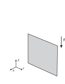
Let us consider the graphene layer in the presence of the external electric field directed along the -axis (see Fig.1).
The emitted current density takes the following form:
| (1) |
where is the electric charge, the Planck constant, the energy, p momentum, the Fermi-Dirac distribution function, the transmission probability of an electron through a potential barrier, and the group velocity. The integrals are over the first Brillouin zone with account taken of the positivity of .
For a two-dimensional (2D) structure, one can use the relation . Moreover, when a graphene sheet has the finite size in the -direction, is quantized. Therefore, the current density in Eq. (1) can be written as
| (2) |
where the Fermi energy is chosen to be zero. Limits and come from the explicit form of the band structure.
We suggest that the transmission probability is given by the WKB approximation in the form Gadzuk
| (3) |
where , , is the work function, the dielectric constant, the electron mass. The function describes a deviation of the barrier from the triangle form due to image effects and can be approximated as (see Ref. Haw ).
The band structure of graphene multilayers has been obtained within the tight-binding approach in Ref. t-b . Besides, an approximation to the dispersion relation can be found from Slonzewski-Weiss-McClure (SWMcC) model for graphite with Bernal stacking SW ; McClure . SWMcC model describes the wave-vector dependence of electron energy in the vicinity of the edge of the Brillouin zone (see Fig.2).

The electron energy spectrum is obtained from the equation
| (4) |
where
| (5) |
and
| (6) |
with , , being the wavevector projection onto the direction , the modulus of the wavevector in the -plain, the angle between and the direction , the distance between nearest neighbour layers, the lattice constant, the momentum in the -plain, and the Fermi velocity. Parameters describe interactions between atoms and is the energy difference between two sublattices in each graphene layer. In Ref. DrH graphite parameters were estimated as and The spectrum of few-layer graphene can be obtained from Eq. (4) by replacing by
| (7) |
where is the number of layers. For graphene bilayer and so that Eq. (4) with account taken of Eq. (7) gives the result of Ref. Mikitik while for (only differs from zero) it reproduces the known tight-binding spectrum of graphene.
As a first approximation one can neglect all interactions except between the nearest-neighbor atoms in the same layer and between A-type atoms between adjacent layers (which are on top of each other), i.e. all parameters except for and are putted to be zero. Then the spectra of multilayers can be approximated by
| (8) |
where .
The FEC and the FEED () are connected by (see, e.g., Ref. Gadzuk )
| (9) |
The explicit form of for few-layer graphene can be found from Eq. (2). Indeed, for layers of a large (infinite) size the sum in Eq. (2) can be replaced by the integral and, correspondingly, one has to use and instead of and . In our case, these -dependent functions can be easily calculated from Eq. (8). Finally, we have to change the order of integration in Eq. (2). The result is
| (10) |
where , , and is the Heaviside step function.
For graphene monolayer one gets
| (11) |
Within the Fowler-Nordheim (FN) approximation (weak fields and low temperatures) the FEC is found to be
| (12) |
where and with (see Ref. Haw ). For bilayer, the FEED is obtained as
| (13) |
and, correspondingly,
| (14) |
where is the MacDonald function. Notice that only the first term in Eq. (13) is significant at weak fields. When the interlayer interaction is weak () Eq.(14) passes into Eq.(12). For large one gets
| (15) |
Thus, we obtain a standard FN exponent while the preexponential factor becomes proportional to instead of for the FN theory. Fig. 3 shows the FEED for different numbers of graphene layers.

Let us now take into account all possible interactions. For this purpose, we use the whole set of SWMcC parameters and put . The numerical results are presented in Fig. 4.

It should be stressed that for and the calculated FEEDs are not sensitive to other interaction constants and curves are found to be identical to those shown in Fig. 3. When increases little shifts of the minima relative to the Fermi energy are obtained. As is clearly seen, for FEEDs have characteristic sub-peaks. The number of peaks and their positions strongly depend on the number of layers and the interaction constants, first of all, . There is a pronounced depression in FEED at the Fermi energy which would be typical for 3D gapless semiconductors.
Fig. 5 gives a clear illustration of our results.

At room temperatures, the Fermi-Dirac distribution function restricts the FEED above the Fermi energy, so that the electron emission from the valence band dominates. The transmission probability decays exponentially with decreasing . Therefore, at fixed one can estimate the energy range of emitted electrons as
| (16) |
In accordance with Fig. 5 the number of emitting channels at the energy is defined as where the brackets indicate integer part. Generally, where is the density of emitting channels. In CNSs is large enough and . In our case, at so that (see Fig. 3). Interestingly that taken into account Eq. (8) one can easily calculate and, correspondingly, for any without integrations. The shape of the FEED in Figs. 3 and 4 directly depends on the density of emission channels. When riches the top of the next branch of the spectrum this branch becomes ”switched-on” thus resulting in a distinctive point in the FEED. Evidently, the closer a position of the branch to the less pronounced is an additional peak in .
An important difference from the emission of single-walled carbon nanotubes should be mentioned. The diameters of CNTs are very small thus resulting in a set of discrete channels. For metallic CNTs there also exists at least one emitting channel at . However, as distinct from CNSs the density tends to a constant value at and, correspondingly, the FEED exhibits behavior typical for conventional metallic emitters without any minimum near the Fermi energy. On the contrary, in semiconducting CNTs the FEED has a characteristic gap at the Fermi energy (cf. Ref. liang2 ).
Similar arguments are valid for the emission from the conduction band where, however, the limiting role of the Fermi-Dirac distribution is of decisive importance. When the temperature grows, the electrons from the conduction band become involved in the emission. As is seen in Fig. 6, the regime of the so-called thermal field emission occurs at high temperatures of emitters.

Notice that there is a rather symmetrical behavior of curves in both bands, which is valid for all considered few-layer structures. Fig. 7 shows an influence of the thermal field emission on the behavior of emission current in the FN coordinates.

The curves are found to be practically identical for any . At high temperatures one can see marked deviations from the standard FN plot in the region of weak fields. Notice that similar deviations were observed in experiments with as-received CNSs (see Fig. 9 in Ref. fecns1 ).
In conclusion, we have calculated the FEED for few-layer graphene films and found the presence of characteristic sub-peaks originated from involving in the emission process additional branches in the energy spectrum of layered structures. Since the peak positions are directly determined by the number of layers the discovery of such peaks in the FEED would be a clear manifestation of the quantum size effect. Therefore, the experimental studies of the FEED for CNSs are very relevant. Furthermore, the FEED analysis gives a new experimental tool to estimate the inter-layer interaction constants (along with Raman scattering in Ref. Malard and photoemission methods in Ref. Ohta ) and provides important information on the concrete types of emitting CNSs as well as allows one to identify the number of layers in emitting CNSs. For example, the absence of sub-peaks would indicate that the emission occurs from monolayer graphene. In addition, the emitter temperature is taken into account in the FEED via the Fermi-Dirac distribution function and can be determined by the half-width and the relative height of shapes in the conduction band. Finally, using an approach suggested in Ref. tfem1 one can measure the resistivity of CNSs.
This work has been supported by the Russian Foundation for Basic Research under grant No. 08-02-01027.
References
- (1) J. J. Wang et al., Appl. Phys. Lett. 85, 1265 (2004).
- (2) J. J. Wang et al., Carbon 42, 2867 (2004).
- (3) M. Bagge-Hansen et al., J. Appl. Phys. 103, 014311 (2008).
- (4) Kun Hou et al., Appl. Phys. Lett. 92, 133112 (2008).
- (5) Goki Eda et al., Appl. Phys. Lett. 93, 233502 (2008).
- (6) A. Malesevic et al., J. Appl. Phys. 104, 084301 (2008).
- (7) J. W. Gadzuk and E.W. Plummer, Rev. Mod. Phys. 45, 487 (1973).
- (8) A. Mayer, N. M. Miskovsky, and P. H. Cutler, J. Phys.: Condens. Matter 15, R177 (2003).
- (9) D. Stark and P. Zwicknagl, J. Appl. Phys. 21, 397406 (1980).
- (10) J. K. Wysockia and D. Stark, Surf. Sci. 247, 402 (1991).
- (11) S. Johnson, U. Zülicke, and A. Markwitz, J. Appl. Phys. 101, 123712 (2007).
- (12) S.-D. Liang et al., Appl. Phys. Lett. 85, 813 (2004).
- (13) V. L. Katkov and V. A. Osipov, J.Phys.: Condens. Matter 20, 035204 (2008).
- (14) S. Latil and L. Henrard, Phys. Rev. Lett. 97, 036803 (2006).
- (15) P. W. Hawkes and E. Kasper, Principles of Electron Optic, (Academic Press, London, 1989), Vol. 2.
- (16) B. Partoens and F. M.Peeters, Phys. Rev. B 74, 075404 (2006).
- (17) J. C. Slonzewski and P. R. Weiss, Phys. Rev. B 109, 272 (1958).
- (18) J. W. McClure, Phys. Rev. B 108, 612 (1957).
- (19) M. S. Dresselhaus and G. Dresselhaus, Adv. Phys. 30, 139 (1981).
- (20) G. P. Mikitik and Yu. V. Sharlai, Phys. Rev. B 77, 113407 (2008).
- (21) S.-D. Liang et al., Phys. Rev. B 73, 245301 (2006).
- (22) L. M. Malard et al., Phys. Rev. B 76, 201401(R) (2007).
- (23) T. Ohta et al., Phys. Rev. Lett. 98, 206802 (2007).
- (24) S. T. Purcell et al., Phys. Rev. Lett. 88, 105502 (2002).