Quantum charge transport in Mo6S3I6 molecular wire circuits
Abstract
Charge transport measurements on flexible Mo6S3I6 (MoSI) nanowires with different diameters in highly imperfect 2-terminal circuits reveal systematic power law behaviour of the conductivity as a function of temperature and voltage. On the basis of measurements on a number of circuits we conclude that the behaviour in thin wires can be most convincingly described by tunneling through Tomonaga-Luttinger liquid (TLL) segments of MoSI wire, which is in some cases modified by environmental Coulomb blockade (ECB). The latter are proposed to arise from deformations or imperfections of the MoSI wires, which - in combination with their recognitive terminal sulfur-based connectivity properties - might be useful for creating sub-nanometer scale interconnects as well as non-linear elements for molecular electronics.
I Introduction
While the transport properties of one-dimensional systems have been of great interest from the point of view of fundamental physics for some timeTLL , recently, further interest in the transport properties of nano-scale one-dimensional systems was aroused because of their importance for the development of molecular electronics, where diverse molecular devices (switches, memory elements, sensors) all need to be self-assembled together with electrically conducting molecular-scale wires. To be of practical use, the connectors need to have reliable contacts and also be able to withstand mechanical deformations while retaining their conducting properties. Till now there has been no recognized material which could be used for this purpose, and this has seriously impeded progress in the development of large scale molecular electronics in recent years.
In this paper we investigate the transport properties of Mo6S3I6 molecular wiresMihailovic , which have been recently shown to be very promising flexible molecular-scale conductors. Mo6S3I6 wires are air-stable one-dimensional inorganic cluster polymers (see Fig.1), which are unique in that they enable covalent bonding to gold surfaces and organic molecules via sulphur atoms at the ends of each molecular wirePloscaru . Single molecular wires were also recently shown to self-assemble gold particles into critical scale-free networks Strle . Such molecular wires may expect their electron transport properties to be governed by quantum properties on the microscopic level. Thus, to make further progress in molecular electronics with MoSI connectors, we must first investigate and understand their molecular scale electronic transport properties. Earlier experimental work has shown metallic signatures, such as a low-frequency Drude response in the optical conductivityVengust , but relatively low room temperature conductivities S/m, which decrease with decreasing temperatureUplaznik . Recently Venkataraman, Hong and Kim Kim described electron transport measurements in multichannel Li2Mo6Se6 nanowires with diameters in the range 7.2 to 12 nm in terms of a Tomonaga-Luttinger liquid (TLL) in contact with Fermi liquid (FL) electrodes. In another related material NbSe3, nanowires ranging between 30 and 300 nm in diameter have been observed to display similar power-law behaviour, albeit over a rather limited range of temperatureSlot . The extreme one-dimensional nature of the MoSI wires suggests that signatures of TLL behaviour might also be observed in thick multi-strand bundles, and not only in very thin wires. On the other hand, we may expect that the electronic transport properties in MoSI wires might depart from ideal TLL behaviour because of the deformable nature of the S bridges which link together the Mo6 clusters into 1D chains Vilfan .
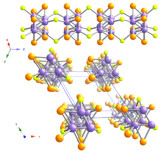
In this paper we present a systematic study of MoSI wires of different diameter from 4 nm to 1000 nm, examining the -dependence, diameter dependence and current-voltage characteristics at different temperatures. We are particularly interested in the behaviour of realistic circuit configurations, with irregular wire geometries. The intrinsic flexibility of the MoSI wires, arising from their accordion-like structure Meden ; Nicolosistructure means that they bend easily to conform to surface contours. We have therefore focused on dielectrophoretically deposited thin wires over contacts in which the wires conform to the surface relief.
Considering the possible transport mechanisms, we confine ourselves to the common ones discussed in literatureKim ; Slot , namely TLL tunnelingTLL , environmental Coulomb blockade ECB (ECB) and variable range hopping (VRH) in the presence of Coulomb charging effects VRH :
1. The and dependence for tunneling into a 1D TL liquid via Fermi-liquid metal contacts is given by:
| (1) |
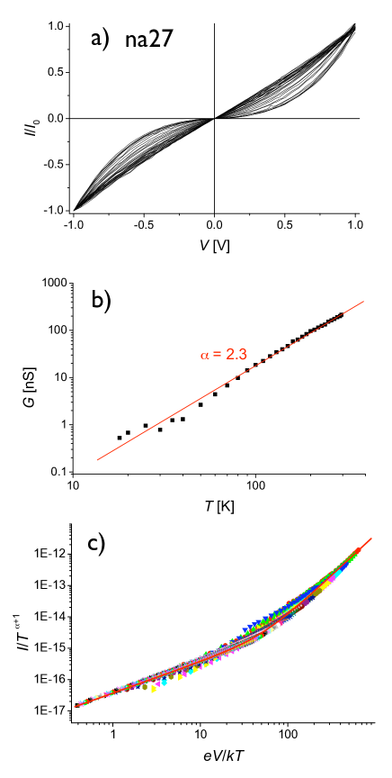
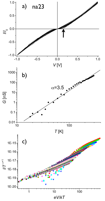
where and the Luttinger parameter . is a fitting parameter that accounts for the voltage drop over the circuit Bockrath ; Kim . A collapsed diagram of the underlying transport characteristic is obtained by plotting against , where is the slope of zero voltage conductivity against temperature . is the exponent for the high voltage limit () arising from the power law behavior .
2. Unfortunately ECB models cannot be solved analytically for the general case, but the asymptotic behavior is very characteristic. The experimentally obtainable low-temperature behaviour is given by:
| (2) |
where is the charging energy, , G is the frequency-independent conductance, and is the tunneling resistance.ECB For low voltages and temperatures the current follows a power law behavior . For high voltages (but low temperatures),
| (3) |
which gives a linear dependence at high V, so the derivative is expected to approach an asymptotic constant value of . ECB ; Uplaznik It also gives a non-zero intercept for given by the charging energy .
3. For the variable range hopping mode, a plot of (for low voltage) against yields curves which become linear with the correct hopping exponent . The fits to the data typically give a large error in the exponents, so to extract the best value of , fits to the data are tested statistically by calculating Pearson’s correlation coefficients.
Rather than choosing a few measurements which obey one or another type of behaviour, we present here a summary of a number of experiments, to try and understand the different types of behaviour that can arise in nanoscale circuits with MoSI wires.

II Experimental details
The thin wires were prepared according to the method reported by Nicolosi et al Nicolosi by repeated dispersion and dilution. The dispersion procedure separates the wires into two distinct categories: thin wires, with diameters nm and thick multichannel bundles with nmNicolosi . In the ultrasonic bath processing procedure, the defective wires break up into shorter segments, leaving less defective long thin wires in solution. The individual strands within the thin wires may thus be expected to have significantly fewer imperfections than within the thick bundles, which may result in different electron transport behaviour in thick and thin wires. This should be evident in the room temperature conductivity () as well as the -dependence and systematics.
The wires were dielectrically deposited typically over nickel electrodes prepared by electron beam lithography (EBL) by placing a drop of solution over the electrodes and applying a 50Hz AC electric field to the electrodes. The entire circuits were then annealed in vacuum at 700 C for an hour. The circuits after annealing are shown in Figure 2. Typical resistances of the nanowires at room temperature were between 100k and 100M. Care was taken to ensure good thermal contact of the sample with the cryostat cold finger.
III Experimental results and analysis
Thin wires
Two thin wire circuits labeled na27 and na23 (shown in Fig. 2) illustrate the most common type of behaviour observed in a number of measured circuits with diameters ranging from to 15 nm. The room-temperature conductivity for na27 and na23 was 3710 S/m and 11900 S/m respectively. Their characteristics at temperatures between 18 K and 300K are shown in Figs.3a) and 4a) and exhibit qualitatively different behaviour. In the case of sample na27, the I-V curves show characteristic inverted S-shaped curves whose curvature is strongly T-dependent. In contrast, circuit na23 shows a clear J-like shape characteristic. (Other circuits we have measured show behaviour in between these two extremes MUThesis ). The -dependence of the conductance at is shown in Figs. 3b) and 4b). The line is a fit to a power law where and respectively. The data follow the power law fit reasonably well, but do not give a perfect fit over the entire range of T. Plotting the entire data set against according to the TLL prediction, for na27 we see that the data collapse quite well onto a single curve (Fig. 3c), where is obtained from the fit. The behaviour of na23 is very different to na27. It gives no such TLL collapse (Fig. 4c), indicating clear departure from TLL predictions. (Overall, approximately half our circuits showed the TLL collapse.)
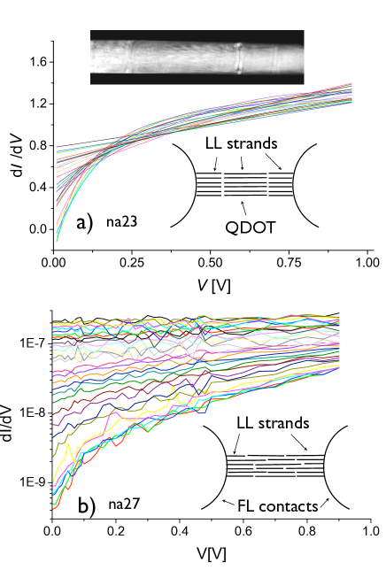
Attempting to fit the ECB model to the data, we would expect the slope to cross over from at low voltages to at high voltages. Correspondingly, the derivative should show a systematic -independent cross-over from to 0 corresponding to the low and high voltage limits respectively. We plot vs. , in Figs. 5 a) and b) respectively for na23 and na27. Circuit na27 shows a rather small variation of with V over the entire range of and (note the small values on the log scale on the axis), quite unlike the ECB model predictions. In contrast, na23 shows a systematic variation with , which for low temperatures is not far from what is expected on the basis of ECB theory: at low , (within experimental error), but clearly saturating at high .
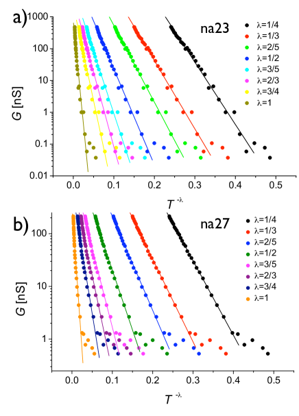
For completeness, attempting to fit the data to the VRH model, we first plotted (for low voltage) against for different =1/4 to 1, according to the VRH model (Fig.6). Making a statistical evaluation using Pearson’s correlation test, we find that the best fit is with for na27 and for na23. Such small values of within VRH models would imply the dominance of 3D hopping processes, which is not expected. (We shall discuss the implications later).
Thick bundles
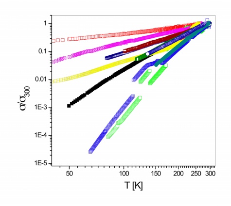
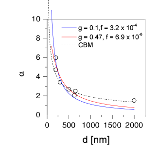
A ubiquitous feature of the thick wire bundles () is their linear I-V characteristic from 18K to 300K Uplaznik . The room temperature conductivity is typically 3 orders of magnitude smaller than for the thin wires, around 1-10 S/m. This is taken as a clear indication that only a small fraction of the molecular strands in the bundle contribute to the transport. Confirming earlier preliminary measurements, the T-dependence was not very well described by a 1D VRH modelUplaznik . The new systematic data on many circuits now confirms this. The dependence of the conductivity is shown in Figure 7 for a number of bundles of different diameter. Surprisingly, the data for the different bundles all appear to follow power-law behaviour quite well. Moreover, a systematic trend is observed, whereby the larger diameters have a smaller exponent , an indication that the numbers of conducting channels scales with diameterTLL (Figure 8).
IV Discussion
The present set of experiments shows a rather wide range of behaviour, suggesting caution in trying to interpret the data by any single model. Discussing the simple VRH model first, our fits give 3D exponents, which is clearly inconsistent with the nature of the system investigated here and is dismissed from further discussion. The calculation of Fogler et al. VRH considered a quasi-1D wire with a finite density of impurities modeled by a series of weakly coupled quantum dots. They predict power law behaviour of the current for both T and V, as at high and at low with . The model holds for a large number of parallel statistically independent conduction channels, where power laws are not obscured by the fluctuations of G. This case is fulfilled here for thick wires, with bundle diameters between 100 nm and 1 might have to conducting channels. However, the prediction that is not fulfilled here for either the thin or the thick multichannel bundles, suggesting that this model may not be applicable for describing MoSI circuits.
In circuit na 27 the TLL prediction can be confirmed with some degree of confidence by the collapsed plot of vs. . For tunneling from a Fermi liquid into a perfect TLL without defects, the model prediction is that . Imperfections, such as deformations and kinks or stoichiometric defects break up the wire into TLL segments, which introduces TLL-TLL tunneling between these segmentsKim , for which the predicted ratio changes to . The measured value for na27 is . A similar circuit with a wire diameter of 5 nm (na12, not shown) gives a near-identical collapse as na27 with .
The exponent for a -channel wire is given by TLL theoryMG as:
| (4) |
where is the electron-electron interaction parameter. The number of conducting channels in a nanowire of diameter can be written as , where is the lattice constant, and is the fraction of molecular wires which actually carry current without interruption. For circuit na27, using , , and channels (for nm), we calculate . This is slightly larger than the value 0.15 obtained by Venkataraman et al for Li2Mo6Se6 nanowires. Other wires which we have measured have between 2 and 3.5, giving a range of . Comparing this with estimated from materials parameters, we can use the expression from the Coulomb charge screening modelMG , where m/s is the Fermi velocity calculated by DFT calculations, is the resistance quantum and the single wire capacitance per unit length is . Using for the Si oxide layer of thickness nm, we obtain . In this estimate, the DFT value of is likely to be overestimated, which may account for a large part of the discrepancy between the values obtained directly from the measurements. It has also been noted previously that the static Coulomb screening model overestimates Kim .
The data in Figure 8 for the thick wires can be fit using the expression (4). A range of values of can be obtained from the fits to the present data, with corresponding filling factors . Values outside this range of cannot be made to fit the data. However, since the characteristics are ubiquitously linear, for the thick wires, this in itself cannot be taken as proof for TLL behaviour.
The low value of in thick wires is assumed to be related to imperfections on the wires. It suggests that the transport along the wires is dominated by tunneling between TLL segments. In fact the resistance of both thick and thin wires is typically of the same order of magnitude, which suggests that in the thick bundles only a very small number of wires are uninterrupted, or that only strands on the outside of the bundle are conducting, with the inner strands being unreachable due to the extremely small perpendicular inter-molecular hopping rates within each wire.
Turning to the case of na23, which shows clear characteristics of ECB behaviour, the intercept of the curve at gives V and consequently F. Comparing this QDOT capacitance with an estimate of C for a single wire over a Si ground plane with a 600 nm SiO2 insulating layer and length nm between contacts, we have , for na23. Depending on what we assume for the QDOT shape, its size appears to be some fraction () of the distance between the electrodes.
Considering the possible origin of the ECB behaviour and the observed departures from the predicted TLL characteristics, we can imagine imperfections and breaks of continuity in the wires of diverse origin. The most obvious and unavoidable effect arises from the deformation of the nanowires adapting to the relief of the contacts (Figure 2). Their inherent flexibility allows for a substantial deformation, which is accompanied by significant changes in electronic structure near the Fermi energy Vilfan ; Tomanek . We can thus envisage that the deformations can lead to breaks in the continuity of individual channels, and as a result the formation of a QDOT in between the breaks. In this case the ECB capacitance would scale with the distance between electrodes. Another effect, which might be important arises from the intrinsic tendency of the wires to form discontinuities in the structure, as shown in the HRTEM image in Figure 5 a). Clear stripes are sometimes observed across the wire bundles, which arise from from stacking faults which appear during the growth process. Indeed such compositional ordering has been recently theoretically predictedYang . HRTEM diffraction analysis shows that the structure of the wire is identical on both sides of the fault, but clearly continuity is broken at these points. Sections in between the faults may thus act as QDOTs, leading to the ECB behaviour we observe. Considering that the distance between faults may be a few tens of nanometers, the comparison of QDOT capacitance with the static capacitance calculated in the previous paragraph suggests this effect may also be important.
V Conclusion
One of our objectives has been to determine how imperfect, bent and deformed MoSI wires might behave in molecular-scale circuits such as may form upon self-assemblyStrle . It is clear from the present experiments that quantum transport dominates their behaviour. The TLL model with its characteristic data collapse of the characteristics at different temperatures appears to hold well for a significant proportion of the thin wire circuits. At the same time clear signatures of the ECB predicted J-shaped curves are also occasionally observed. Discontinuities in the wires either as a result of bending, and/or structural stacking faults within the wire are believed to cause the formation of QDOTs, which lead to the occasional occurrence of ECB behaviour. The diameter of the present MoSI wire bundles is small enough to allow covalent S bonding to individual moleculesPloscaru , so for the construction of molecular scale circuits, where thin and relatively short wires are of interest, they may potentially revolutionize molecular electronics. A point of interest is the possibility of making variable sizes of QDOTs with MoSI wires by stretching them over appropriately sized regular topological features to produce arrays of QDOTs. The other possibility of creating single QDOTs by using the tip of an atomic force microscope, was already recently demonstrated Abdou .
We wish to thank D.Vengust for providing samples of MoSI nanowires and J.Strle for proof reading the manuscript.
References
- (1) J. Voit, Reports on Progress in Physics 58, 977 (1995) and references within.
- (2) D.Vrbanic et al., Nanotechnology 15, 635 (2004), for a review, see: D.Mihailovic, Rep. Materials Science 54, 309 (2009)
- (3) I.M. Ploscaru, S. Jenko Kokalj, M. Uplaznik, D. Vengust, D. Turk, A. Mrzel, D. Mihailovic, Nanoletters, 7, 1445 (2007).
- (4) J.Strle, D.Vengust and D.Mihailovic, Nano Letters 9, 1091 (2009)
- (5) D. Vengust, F. Pfuner, L. Degiorgi, I. Vilfan, V. Nicolosi, J.N. Coleman, D. Mihailovic, D.D., Physical Review. B: Condensed Matter, 76, 075106 (2007)
- (6) M. Uplaznik, B. Bercic, J. Strle, M.I. Ploscaru, D. Dvorsek, P. Kusar, M. Devetak, D. Vengust, B. Podobnik, D. Mihailovic, Nanotechnology, 17, 5142 (2006), B.Bercic et al Appl. Phys. Lett. 88 173103 (2006)
- (7) L. Venkataraman, Yeon Suk Hong, P.Kim, Phys. Rev. Lett., 82, 4918 (1999).
- (8) E. Slot, M.A. Holst, H.S.J. van der Zant, S.V. Zaitsev-Zlotov, Physical Review Letters, 93, 176602 (2004).
- (9) I. Vilfan, D. Mihailovic, Physical Review B, 74 235411 (2006)
- (10) Nicolosi et al., Adv Mater 19, 543 (2007)
- (11) T.Meden et al, Nanotechnology 16, 1578 (2005)
- (12) M.C. Bockrath, H. David, J. Lu, A. Rinzler, R.E. Smalley, L. Balents, P/I/ McEuen, Phys. Rev. Lett., Nature, 397, 596 (1999).
- (13) H. Grabert, M.H. Devoret, NATO ASI Series B, 294, (1992)
- (14) V. Nicolosi, D. Vrbanic, A. Mrzel, J. McCauley, S O’Flaherty, C. McGuinness, G. Compagnini, D. Mihailovic, W.J. Blau, J.N. Coleman, The Journal of Physical Chemistry. B, 109 7124 (2005)
- (15) M.M Fogler, S. Teber, B.I. Shklovskii, Physical Review. B, 35 035413 (2004)
- (16) K.Matveev and L.Glazman, Phys.Rev.Lett. 70, 990, (1993)
- (17) M.Uplaznik, PhD Thesis, Univ. of Ljubljana (2009)
- (18) A.Hassanien et al., Physica E 29, 684 (2005), H.W.Ch.Postma et al, Science 293, 76, (2001)
- (19) Popov et al. Phys. Rev. Lett. (2007) 99 085503 (2007)
- (20) T.Yang, S.Berber and D.Tomanek, Phys. Rev. B 77,7 (2008)