Silicon surface with giant spin-splitting
Abstract
We demonstrate the induction of a giant Rashba-type spin-splitting on a semiconducting substrate by means of a Bi trimer adlayer on a Si(111) wafer. The in-plane inversion symmetry is broken so that the in-plane potential gradient induces a giant spin-splitting with a Rashba energy of about 140 meV, which is more than an order of magnitude larger than what has previously been reported for any semiconductor heterostructure. The separation of the electronic states is larger than their lifetime broadening, which has been directly observed with angular resolved photoemission spectroscopy. The experimental results are confirmed by relativistic first-principles calculations. We envision important implications for basic phenomena as well as for the semiconductor based technology.
Exploiting the electron spin for information processing is one of the leading goals in the rapidly growing field of spintronics. At its heart lies the Rashba-Bychkov (RB) type spin-splitting, where the spin-orbit interaction lifts the spin degeneracy in a symmetry broken environment Rashba . Many device proposals make use of this concept Sinova ; Datta ; Ohe ; Koga with some interesting proofs of principle Kato ; Wolf . The materials of choice are semiconductor heterostructures, albeit the size of the spin-splitting is typically very small. A large spin-splitting is desirable as it would, for example, decrease the precession time of the spin in a spin transistor Datta so that it is smaller than the spin relaxation time. Furthermore, a separation of the spin-split states beyond their lifetime broadening is an important criterion for distinguishing between the intrinsic and extrinsic spin Hall effect Sinova ; Wunderlich ; Bernevig . The different influences on the intrinsic spin Hall conductivity, such as disorder and elastic/inelastic lifetime, are still under debate Wang ; Yang .
Recently, a giant spin-splitting has been demonstrated for noble metal based surface alloys Ast ; Ast1 ; Ast2 ; Pacile , where heavy elements with a strong atomic spin-orbit coupling are incorporated into the surface. These systems, however, are not suitable for the field of spintronics because of the presence of spin-degenerate bands at the Fermi level originating from the metallic substrate. One possible alternative is to grow thin films with spin-split bands onto a semiconducting substrate Frantzeskakis ; He ; Hirahara . However, due to confinement effects a multitude of quantum well states arise, which potentially influence the transport properties of the system. It is, therefore, desirable to transfer the concept of the giant spin-splitting directly onto a semiconductor surface.
Here we show that a monolayer of Bi trimers on a Si(111) surface forms a two-dimensional (2D) electronic structure with a giant spin-splitting much larger than what has been observed so far at the interfaces of semiconductor heterostructures. The effect can be traced to a strong contribution of an in-plane potential gradient due to an inherent structural inversion asymmetry (RB model). While the structure of this system has been studied both theoretically as well as experimentally Miwa ; Wan ; Shioda , the electronic structure, in particular a possible spin-splitting of the electronic states, has remained a controversial issue Kinoshita ; Kim1 . We demonstrate unequivocally that Bi induces a giant spin-splitting at the silicon surface. Furthermore, the spin-splitting is observed to be larger than the lifetime broadening, so that the Bi/Si(111) system is a prime candidate for spintronics applications or studying the intrinsic spin Hall effect. In addition, the silicon substrate allows for excellent compatibility with existing silicon-based semiconductor electronics.
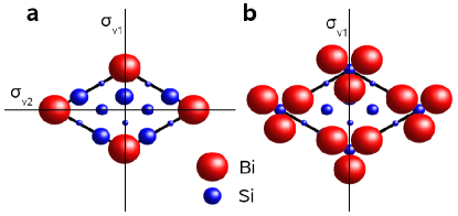
A single layer of Bi on Si(111) grows in a monomer as well as a trimer configuration, both of which show a ()R30∘ reconstruction Miwa ; Wan ; Shioda . A structural model is shown in Fig. 1 for the monomer phase (a) and the trimer phase (b). Both the monomers and the trimers are centered on top of second layer Si atoms ( lattice sites) forming a symmorphic space group based on the point group . The Si substrate breaks the in-plane inversion symmetry for both the monomer and the trimer phase. Looking at the isolated Bi adlayer alone, the trimer formation introduces a reduction of the symmetry because the mirror plane is missing. The mirror plane holds for both the monomer and the trimer phase as well as for the combination of adlayer and Si substrate. From these simple symmetry considerations we conclude that the Bi trimer phase is the least symmetric structure and, hence, should lead to the bigger spin-splitting. We, therefore, only consider the trimer phase. Its preparation was verified with quantitative low-energy electron diffraction measurements EPAPS .
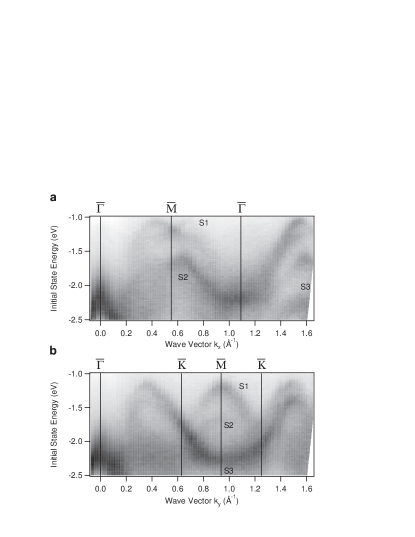
The experimental band structure measured with angular resolved photoemission spectroscopy (ARPES) along the two high symmetry directions of the surface Brillouin zone (SBZ) and is displayed in Fig. 2 (a) and (b), respectively EPAPS . The intense feature near at an energy of about eV can be attributed to the silicon bulk. The other features (S1, S2, S3) in Fig. 2(a) originate from the 2D electronic structure of the surface. S1 is most intense at the -point at an initial state energy of about eV. This band splits in two components when moving away from the high symmetry point , which is a strong indication of a RB-type spin-splitting. S2 is located at about eV at the second -point and disperses upwards towards the -points. The third state S3 shows the highest intensity at the second -point at an energy of about eV. This band moves downwards in energy towards the second -point. The bandwidth of S3 is smaller than the one for S2. These three 2D states are also visible along the -direction as shown in Fig. 2 (b). S1 appears as a parabolic band with negative effective mass with a band maximum located at about eV at the -point. Along the direction no splitting of this band has been observed. S2 is located around eV at , but only with a very weak intensity. The most intense feature along the -direction is the S3 2D state with a band minimum at about eV at the -point and an upwards dispersion towards the neighboring -points.
A possible spin-splitting in the Bi/Si(111) system is an unresolved issue in the literature. While Kinoshita et al. Kinoshita consider a splitting in the three 2D states related to a strong spin-orbit interaction of the Bi atoms, it has been dismissed by Kim et al. Kim1 . In the following, we will show from the experimental data as well as spin-resolved band structure calculations that the band structure shows a giant spin-splitting of the electronic states due to the RB effect.
Spin-degeneracy is a consequence of both time reversal and spatial inversion symmetry. If the latter is broken spin-degeneracy can be lifted by the spin-orbit interaction (RB model) EPAPS . In addition, if the inversion symmetry is also broken in the plane of the two-dimensional electron gas, the contribution from an in-plane gradient can strongly enhance the spin-splitting Ast1 . The characteristic parameters quantifying the strength of the splitting are the momentum offset , the coupling constant in the Hamiltonian (Rashba parameter), as well as the Rashba energy . They are related by and . Here is the effective mass.
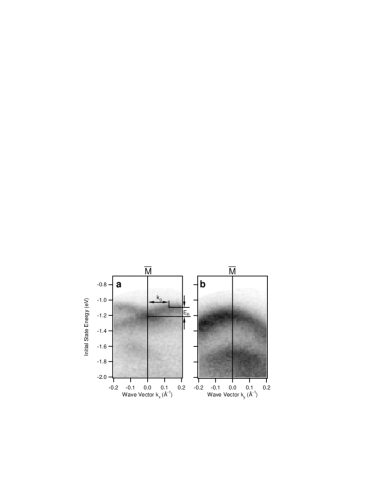
A close up of the band structure near the -point is shown in Fig. 3. The bands along (Fig. 3(a)) near 1.2 eV clearly show the characteristic dispersion of a RB type spin-splitting with the band crossing at the -point and the shift of the maxima away from it. From the data we extract the momentum offset Å-1, an effective mass of ( free electron mass) as well as the Rashba energy meV. From these values we can calculate the Rashba parameter =1.37 eVÅ. The spin-splitting is well resolved in the data. The average line width for the spin-split states at the band maximum (Å-1) is 195 meV, which accounts for intrinsic lifetime as well as interactions and scattering. The separation of the states is about 220 meV.
The spin-splitting at the -point in Fig. 3(a) is strongest along the -direction. Along the -direction in Fig. 3(b) the spin-splitting at the -point is much weaker and cannot be resolved in the experiment. This peculiar band topology can be related to the symmetry properties of the -point. As the -point is located on the border of the first SBZ it has a reduced symmetry as compared to the -point. Despite the symmetry breaking of the Bi trimers, the mirror symmetry (see Fig. 1) holds so that for the dispersion along the -direction the spin-splitting is greatly reduced, i. e. it can not be observed in the data.
To support our interpretation of the observed spin-splitting, we conducted spin-resolved first principles band structure calculations, which were performed in close analogy to our previous calculations on the RB effect Ast1 . The surface geometry of the trimer structure is determined from first principles using the Vienna Ab-initio Simulation Package (VASP) which provides precise total energies and forces Kresse96 . The Bi trimers (milkstool structure) are relaxed outward by from the ideal positions (100% corresponds to the Si bulk interlayer distances, lattice constant ). The subsurface relaxations are small () and neglected in the Korringa-Kohn-Rostoker (KKR) calculations. The in-plane displacement of the Bi trimer atoms is , with indicating Bi on-top of first layer Si atoms and coinciding Bi-trimer atoms on sites. The subsequent KKR and relativistic layer-KKR calculations use the structural data from VASP as input. The spectral density is obtained from the imaginary part of the site-dependent Green function. Resolved with respect to spin orientation (index ) and angular momentum, it allows a detailed analysis of the electronic structure. The difference reveals the characteristic spin splitting of RB-split bands.
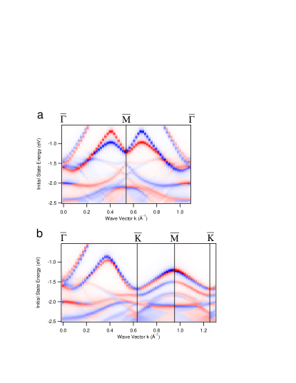
The results of the band structure calculations are shown in Fig. 4 for the -direction in (a) and for the -direction in (b). The intensity scale shows the total spectral density () of the states multiplied by the sign of the spin-polarization sgn() perpendicular to the high symmetry line, i. e. blue and red colors correspond to opposite spin-polarizations. The calculations reproduce all the main features of the measured band structure. In particular, the splitting of the S1 band around the -point along the -direction is well documented. As can be seen in figure 4 the two branches of the split S1 band clearly show opposite spin-polarization, i. e. a giant spin-splitting in the electronic structure of Bi/Si(111).
The spin-splitting is strongly anisotropic around . The peculiar band topology, which was observed in the experiment is clearly reproduced in the calculations. This can again be attributed to the lower symmetry of wave vectors within () or perpendicular () to a mirror plane of the system. It is conceived that this feature results from the ‘trimerization’ of the three Bi sites in the 2D unit cell; calculations with a reduced (i. e. larger distance between Bi trimer atoms) indicate an even smaller splitting along . Furthermore, the calculations show that about 83% of the spin-split states at the -point are localized in the Bi adlayer and about 16% in the first Si layer. One can thus speculate that the spin-splitting is particularly influenced by the Bi adlayer and that trimerization symmetry breaking increases the effect of the in-plane potential gradient.
The giant spin-splitting in the Bi/Si(111) trimer system has a similar origin as in the Bi/Ag(111) surface alloy: An inversion symmetry breaking in the plane of the surface leads to a strong contribution from an in-plane potential gradient, which substantially enhances the spin-splitting. In both systems the threefold symmetry of the underlying substrate breaks the in-plane inversion symmetry. However, considering only the topmost layer, the trimer formation in Bi/Si(111) also leads to a breaking of the in-plane inversion symmetry (see Fig. 1), which is not the case for the Bi/Ag(111) surface alloy.
Comparing the spin-splitting of the Bi/Si(111) electronic structure to semiconductor heterostructures, we find that in the latter the spin-splitting is substantially smaller. For example, for an inverted InGaAs/InAlAs heterostructure a Rashba constant of eVÅ has been measured Nitta . With an effective mass of , a Rashba energy of eV can be calculated. For HgTe quantum wells a Rashba constant eVÅ has been found Schultz . However, here the spin-splitting has been identified to be proportional to instead of a linear dependence Zhang . For the Bi/Si(111) system, the Rashba energy meV as well as the Rashba parameter eVÅ are much bigger. From the momentum offset Å-1 we can calculate that a phase shift of the spin precession angle can be obtained after a length of only nm. In the InGaAs/InAlAs heterostructure a length of 400 nm has been estimated. While these figures show the excellent potential of the Bi/Si(111) system, additional measurements giving insight into the transport properties, such as Shubnikov-de Haas oscillations, are necessary to further elaborate the suitability of this system for spintronics applications. Corresponding experiments are in progress.
We have shown that the trimer phase of Bi on Si(111) shows a giant spin-splitting. The experimental results reveal the characteristic band dispersion of a RB-type spin-splitting with a peculiar band topology at the point. They are confirmed by first principles band structure calculations. The splitting is caused by the spin-orbit interaction induced RB effect in combination with a strong contribution from the in-plane gradient due to the reduced symmetry of the trimer structure and the substrate. Furthermore, this spin-splitting is of the same order of magnitude as the one reported for Bi/Ag(111) and orders of magnitude lager than a typical spin-splitting reported for semiconductor heterostructures. In this way, we have transferred the concept of giant spin-splitting onto a semiconducting substrate. This gives excellent perspectives for the use of this concept in the field of spintronics. In particular, the silicon substrate makes this system compatible with existing semiconductor technology. On the fundamental side such systems are interesting for, e. g., the spin Hall effect. Since the energy separation of the spin-split states (220 meV) is larger than the lifetime broadening (195 meV), it may be easier to distinguish the extrinsic and intrinsic spin Hall effects.
References
- (1) Y. A. Bychkov and E. I. Rashba Sov. Phys. JETP Lett. 39, 78 (1984)
- (2) J. Sinova, D. Culcer, Q. Niu, N. A. Sinitsyn, T. Jungwirth and A. H. MacDonald Phys. Rev. Lett. 92, 126603 (2004)
- (3) S. Datta and B. Das Appl. Phys. Lett. 56, 665 (1990)
- (4) J.-I. Ohe, M. Yamamoto, T. Ohtsuki and J. Nitta Phys. Rev. B 72, 041308(R) (2005)
- (5) T. Koga, J. Nitta, H. Takayanagi, and S. Datta Phys. Rev. Lett. 88, 126601 (2002)
- (6) Y. Kato, R. C. Myers, A. C. Gossard, and D. D. Awschalom, Nature 427, 50 (2004)
- (7) S. A. Wolf, D. D. Awschalom, R. A. Buhrman, J. M. Daughton, S. von Molnár, M. L. Roukes et al. Science 294, 1488 (2001)
- (8) J. Wunderlich, B. Kaestner, J. Sinova, and T. Jungwirth, Phys. Rev. Lett. 94, 047204 (2005).
- (9) B. A. Bernevig, S.-C. Zhang, Phys. Rev. Lett. 95, 016801 (2005).
- (10) P. Wang and Y. Q. Li, J. Phys.: Condens. Matter 28, 215206 (2008) and references therein.
- (11) W. Yang, K. Chang, and S. C. Zhang, Phys. Rev. Lett. 100, 056602 (2008) and references therein.
- (12) C. R. Ast, D. Pacilé, M. Falub, L. Moreschini, M. Papagno, G. Wittich, P. Wahl, R. Vogelgesang, M. Grioni, K. Kern, cond-mat/0509509 (2005).
- (13) C. R. Ast, J. Henk, A. Ernst, L. Moreschini, M. C. Falub, D. Pacilé, P. Bruno, K. Kern and M. Grioni Phys. Rev. Lett. 98, 186807 (2007)
- (14) C. R. Ast, G. Wittich, P. Wahl, R. Vogelgesang, D. Pacilé, M. C. Falub, L. Moreschini, M. Papagno, M. Grioni and K. Kern Phys. Rev. B 75, 201401(R) (2007)
- (15) D. Pacilé, C. R. Ast, M. Papagno, C. Da Silva, L. Moreschini, M. Falub, A. P. Seitsonen, and M. Grioni, Phys. Rev. B 73, 245429 (2006).
- (16) E. Frantzeskakis, S. Pons, H. Mirhosseini, J. Henk, C. R. Ast, and M. Grioni, Phys. Rev. Lett. 101, 196805 (2008).
- (17) K. He, T. Hirahara, T. Okuda, S. Hasegawa, A. Kakizaki, and I. Matsuda, Phys. Rev. Lett. 101, 107604 (2008).
- (18) T. Hirahara, T. Nagao, I. Matsuda, G. Bihlmayer, E. V. Chulkov, Yu. M. Koroteev, P. M. Echenique, M. Saito, and S. Hasegawa, Phys. Rev. Lett. 97, 146803 (2006).
- (19) R. H. Miwa, T. M. Schmidt and G. P. Srivastava J. Phys.: Condens. Matter 15, 2441 (2003)
- (20) K. J. Wan, T. Guo, W. K. Ford and J. C. Hermanson Surf. Sci. 261, 69 (1992)
- (21) R. Shioda, A. Kawazu, A. A. Baski, C. F. Quate, and J. Nogami, Phys. Rev. B 48, 4895 (1993)
- (22) see EPAPS Supporting Information
- (23) T. Kinoshita, S. Kono and H. Nagayoshi J. Phys. Soc. Jpn. 56, 2511 (1987)
- (24) Y. Kim, J. S. Kim, C. C. Hwang, S. P. Shrestha, K. S. An, and C. Y. Park J. Kor. Phys. Soc. 39, 1032 (2001)
- (25) G. Kresse and J. Furthmüller, Phys. Rev. B 54, 11169 (1996)
- (26) J. Nitta, T. Akazaki, H. Takayanagi, and T. Enoki, Phys. Rev. Lett. 78, 1335 (1997)
- (27) M. Schultz, F. Heinrichs, U. Merkt, T. Colin, T. Skauli, and S. Løvold, Semicond. Sci. Technol. 11, 1168 (1996)
- (28) X. C. Zhang, A. Pfeuffer-Jeschke, K. Ortner, V. Hock, H. Buhmann, C. R. Becker, and G. Landwehr, Phys. Rev. B 63, 245305 (2001)
Supporting Information
Sample preparation
The sample preparation as well as the measurements were conducted in ultra high vacuum (UHV) with a base pressure of mbar. The n-doped Si(111) substrate was annealed at 1100∘C by direct current heating for 10 minutes and cooled down slowly to 800∘C over a time interval of 10 minutes until a sharp (77) low energy electron diffraction (LEED) pattern was observed. One monolayer (ML) of Bismuth was deposited at a substrate temperature of 470∘C using a commercial electron beam evaporator to form an adlayer of trimers. The substrate temperature was measured with an optical pyrometer. After Bi-deposition LEED measurements showed a ()R30∘ reconstruction.
Quantitative LEED measurements
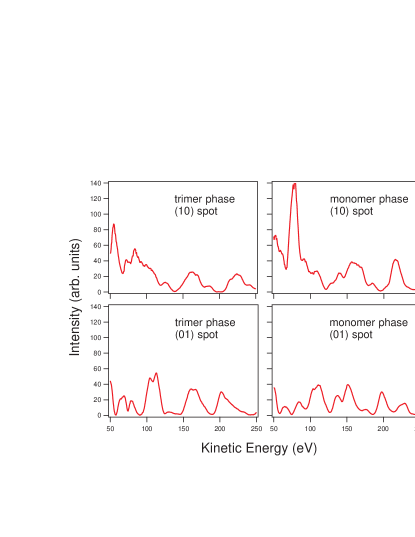
As both the monomer phase at 1/3 ML Bi coverage and the trimer phase at 1 ML Bi coverage show the same ()R30∘ reconstruction we used quantitative LEED measurements to distinguish between the two phases. We measured the integrated intensity of the (10) and (01) spots as a function of electron energy and compared them to calculations done by Wan et al. Wan . The measured data was averaged over three equivalent spots and smoothed. The result is shown in figure 5. The agreement between measured and calculated spectra is quite convincing, allowing an unambiguous identification and preparation of the trimer phase.
STM measurements
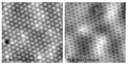
In figure 6 two (1010)nm2 topographic STM images are shown. In (a) the monomer phase is of the Bi/Si(111) structure is shown at a bias voltage of 1.55 V and a tunneling current of 0.2 nA is shown. In (b) the trimer phase is shown at a bias voltage of 0.95 V. The tunneling current was 0.2 nA as well.
Band structure measurements
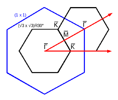
Angle-resolved photoemission spectroscopy (ARPES) measurements were done with a hemispherical SPECS HSA3500 electron analyzer with an energy resolution of 10meV. The images were recorded with a step size of 1∘ in angular direction. We used monochromatized He I radiation with an energy of 21.2 eV for the ARPES measurements. The sample was kept at 90 K during the measurements. We measured the band structure along the two high symmetry directions and of the surface Brillouin zone (SBZ) associated with the ()R30∘ reconstruction (see Fig. 7).
The zero for the initial state energy in the measured data was set to the Fermi level. We chose an n-doped Si substrate because the position of the Fermi level is close to the conduction band. This allows states within the bulk band gap to be easily accessible by photoemission spectroscopy. From the recorded data we subtracted a Shirley background and normalized every energy distribution curve (EDC) of the image to the same integrated intensity.
Rashba-Bychkov model
Spin-degeneracy is a consequence of both time reversal and spatial inversion symmetry. If the latter is broken spin-degeneracy can be lifted by the spin-orbit interaction. For a free electron gas in two dimensions the spin-orbit coupling Hamiltonian in the Rashba-Bychkov (RB) model is given by the following equation Rashba :
where the coupling constant is called Rashba parameter, are the Pauli matrices, is the in-plane momentum and is a unit vector normal to the plane of the two dimensional electron gas (2DEG). The resulting energy dispersion is:
with the effective mass , the offset in parallel momentum and the band extremum at . The RB Hamiltonian lifts the spin-degeneracy and introduces an offset in parallel momentum of the nearly free electron parabola. At high symmetry points the bands are degenerate due to time inversion symmetry. As a result the band dispersion of a RB split band has a very characteristic shape. The Rashba parameter in the most straight forward formulation of the RB Hamiltonian is proportional to the potential gradient perpendicular to the plane of the 2DEG. An additional contribution from an in-plane gradient can strongly enhance the spin-splitting.
From the photoemission data the Rashba energy (the energy difference between the crossing point of the two parabolas and the band extremum), the offset of the two parabolas in parallel momentum and the effective mass can be determined. These parameters are related to an effective Rashba-parameter via
| (1) |
This effective Rashba parameter contains all the different contributions to the spin-splitting, i. e. the potential gradient in the plane of as well as perpendicular to the surface and the atomic spin-orbit coupling from the atoms involved. The Rashba parameter determined from equation (1) should be understood as a characteristic parameter for comparison with other systems.
References
- (1) K. J. Wan, T. Guo, W. K. Ford and J. C. Hermanson Surf. Sci. 261, 69 (1992)
- (2) Y. A. Bychkov and E. I. Rashba Sov. Phys. JETP Lett. 39, 78 (1984)