Quantum Confinement and Phase Transition in PbS nanowire
Abstract
We report first principles density functional calculations of electronic structures and energy bandgaps () in PbS nanowires (NW). The is tuned by varying the diameter of the NW - revealing the role of quantum confinement. The compressive radial strain (CS) on the NW is shown to be responsible for semiconducting to metallic phase transition. The conduction band (CB) of the NW, which has significant contribution from the excited 3d-orbital of S, is found to be more sensitive to the CS with the CB minimum shifting towards and eventually crossing the Fermi energy with increasing CS. The origin of the observed phase transition in a recent experiment is attributed to the CS on the PbS nanowire.
pacs:
73.63.-b, 85.65+h, 73.50.Fq, 71.10.-wI INTRODUCTION
One dimensional nanowires have become the foremost candidates in building nano transistor, optoelectronic devices, nano sensors, nano electrodes and logic circuits logic-gate ; Zhong ; nano-circuit ; virus ; science ; Markreed . One of the key features that dictate their suitability in these applications is their tunable electronic structure property and hence their energy band gap. In recent years, II-VI PbS hetero nanowire (NW) structures have drawn considerable interest for their potential applications in optical switches switch ; photovoltic and solar cells solarcell ; solarcell1 . Controlled synthesis of PbS nanowires with diameters ranging from 1.2 nm to 10 nm have been reported somo ; prb ; nanolett . This presents exciting opportunities to explore the tunable electronic structure property of this material in the strong quantum confinement regimeprl1 ; tapered ; InP ; Jena ; Molyb ; PbSe ; PbSnTe ; Iop . PbS in the bulk phase has a cubic close packed (CCP) structure with a near infrared direct band gap of 0.41 eV at the L point bulk . Current photo luminescence study reveals wide band gap for PbS nanowires due to a higher degree of quantum confinement somo . Furthermore, PbS nanowires of diameter 1.2 nm grown in Na-4 Mica channels have been found to exhibit semiconducting to metallic phase transition at 300 K prb . The thermal expansion mismatch at PbS and Na-4 Mica interface producing 3 GPa pressure on the nanowire, has been suggested as the cause for this phase transition.
Despite these progresses made in the last few years in controlled synthesis of PbS nanowires, no theoretical calculations have been reported on these systems to understand the quantum confinement effect and the origin of the observed phase transition phenomenon. In this letter, we have made the first attempt to elucidate the tunable confinement effect in PbS nanowire as well as the origin of the phase transition from electronic structure calculations. We have used the first principles density functional theory to study the variation of the energy band gap () with the diameter of PbS nanowire. By varying the diameter(d) of the nanowire from 1.17 nm to 3.64 nm, the is found to change from 1.524 eV to 0.955 eV; this is substantially higher than the of 0.4 eV observed for the bulk PbS - clearly revealing the role of the quantum confinement. The reduced Pb-S bond length in the 1.17 nm diameter NW as compared to that in the 3.64 nm wire leading to a more confined charge density is found to be responsible for the observed increase in the with the decrease of ‘d’ of the wire. The compressive radial strain (CS) is found to have a profound effect on the electronic properties of the NW. A semiconducting to metallic phase transition is observed when the PbS nanowire is exposed to a particular CS. The inward radial strain changing strength of the p-d hybridization between the Pb and S atoms is accountable for the metallic behavior in the strained nanowire. Thus we have identified that the observed phase transition is due to the compressive lattice strain, which may have been caused by the thermal expansion mismatch at the PbS and Na-4 Mica interface as suggested by the experiment prb . Besides, the evolution of with radial strain offers a tantalizing route to tune the electronic and optical properties of these nanowires. The strained nanowire is found to exhibit indirect band gap behavior while the unstrained nanowire has a near direct band gap property. The calculated radial Young’s modulus and the pressure for phase transition in a representative nanowire of d 1.98 nm are found to be 857 GPa and 102.8 GPa respectively.
The rest of the paper is organized as follows. In Sec. II, a brief description of the computaional procedure is given. Results and discussions are presented in Sec. III followed by a brief summary in Sec. IV.
II COMPUTATIONAL PROCEDURE
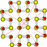
As atomic level structural details of the PbS NWs are not available a priori, we used the CCP PbS structure as the guiding point and constructed the 1D nanowire in the observed [200] growth direction. We selected two layers from the bulk structure with twelve Pb atoms and twelve S atoms and placed them in a tetragonal unit cell with guess lattice parameter along the z-axis to construct the unit cell of the NW. To avoid interaction between the NW and its image in the x and y- directions, we have taken a relatively large lattice parameter of 1.89 nm along those two directions. Subsequently, the NW structure is optimized. The optimum value of is found to be 0.60 nm. The same procedure is used to obtain the equilibrium NW structure for other three NWs of d 1.98 nm, 2.80 nm, and 3.64 nm, containing 64, 120 and 192 atoms in the unit cell respectively. The optimum value (0.60 nm) is found to be insensitive to the diameter of the NW. The lattice parameter for the PbS nanowire of diameter 100 nm reported from a recent experiment pbsexpt is 0.597 nm, which is in excellent agreement with our calculated value of 0.60 nm. The average distance between two Pb atoms or two S atoms located at two corners of the optimized unit cell (shown in Fig. 1 by the dotted line) is calculated, and the Covalent radii of Pb and S are added appropriately to the average distance to estimate the diameter of the NW. We have used the plane wave basis functions and periodic density functional approach within the generalized gradient approximation (GGA) for the exchange-correlation. The valence-core interaction is described by the projector-augmented wave (PAW) approach. Computations are carried out using Vienna ab-initio simulation (VASP) code vasp . To determine the optimized structure, we have used a (4 irreducible k-points) k-point grid within the Monkhorst-Pack (MP) scheme to sample the Brillouin zone. To check the accuracy and convergence of our results, we have also performed structural optimizations of the NW by using and k-point grids within the MP scheme. The relative difference in Cohesive Energy by increasing the irreducible k-points from 4 to 6 is found to be 0.001 while the relative difference in band gap energy is 0.01 . We consider the structure to be optimized when the force on an individual atom is eV/. The convergence criterion for the energy during the self-consistent calculation is taken to be eV. The energy cut off for the plane wave basis is 280 eV.
III RESULTS AND DISCUSSIONS
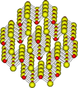
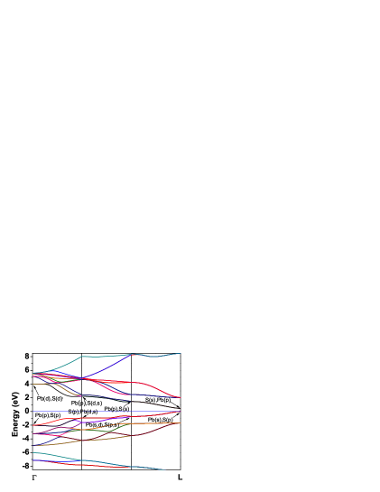
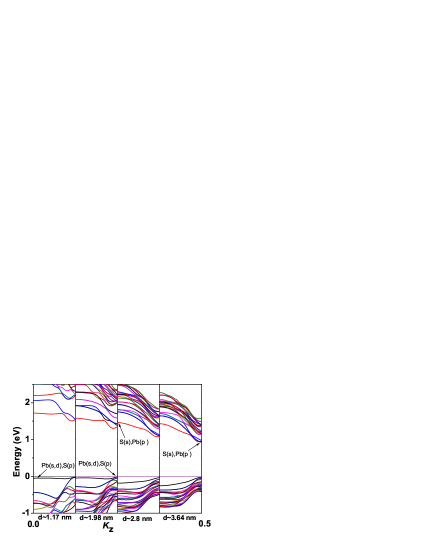
First, we have performed energy band structure calculations for the PbS bulk structure to calibrate our computational approach. We have used k-point grid within the MP sceme to sample the brillouin zone (BZ). The energy band diagram is summarized in Fig. 2(a). One can notice from Fig. 2(a) that the PbS in the bulk phase is a direct band gap semiconductor. The optimum lattice parameter is 5.98 . At the L-point the is found to be 0.44 eV. This is in very good agreement with the 0.41 eV for reported from the experiment bulk . It should be noted that the use of k-point sampling within the MP sceme to sample the BZ yields a gap of 0.42 eV at the L-point, suggesting that convergence in is achieved in our calculation with respect to the number of k-points, adding further confidence in our results. As discussed in the previous section, nanowires of different diameters are engineered along the observed [200] growth direction and optimized.The cross sectional view of the optimized unit cell structure from a representative nanowire of diameter 1.98 nm is shown in Fig. 1(a). Fig. 1(b) shows the side view of four unit cells in [200] direction. First, we comment on the stability. To infer the stability of the NW, we have calculated the cohesive energy per atom () for each NW, which is summarized in Table 1. One notes from Table 1 that the maximum difference in between the bulk and the NW is 0.1 eV; this suggests that the stability of the NWs are comparable to that of the bulk. As expected, the difference in between PbS nanowire and bulk PbS decreases as the diameter of the nanowire increases. The difference in between NW of diameter 3.64 nm and bulk PbS is only 0.04 eV. Second, (Table 1) is found to decrease as the diameter of the NW increases. For a NW of diameter 1.17 nm, the energy band gap is found to be 1.524 eV, which decreases to 0.955 eV for a NW with diameter 3.64 nm. More importantly, we found a monotonic decrease in the energy band gap with an increase in diameter. To develop an atomic level understanding of the observed change in , we analyzed the nearest neighbors’ bond length between Pb and S atoms within the x-y plane. As the diameter decreases, the average nearest neighbor distance, l, between Pb and S is found to decrease (Table 1), resulting in a more confined charge density. This higher degree of quantum confinement for a smaller diameter NW is resulting in an increase in its band gap.
| d(nm) | l (nm) | (eV) | |
|---|---|---|---|
| 1.17 | 0.283 | 4.316 | 1.524 |
| 1.98 | 0.286 | 4.356 | 1.299 |
| 2.8 | 0.289 | 4.375 | 1.098 |
| 3.64 | 0.295 | 4.380 | 0.955 |
| Bulk | 0.299 | 4.426 | 0.44 |
To show the diameter dependence of the energy bands, we have plotted the Kohn-Sham energy bands for all four NWs in Fig. 2(b). For larger diameter NW, the minimum energy point in the conduction band (CBM) and the maximum energy point in the valence band (VBM) appear at the same k point. This confirms their direct band gap property as observed in bulk PbS. But when the diameter decreases, the CBM shifts towards the -point, resulting in an indirect band gap behavior. Furthermore, as expected, the degeneracy in the energy bands is lifted as the diameter decreases. The conduction band is found to be more sensitive to the decrease in diameter. It should be noted that, very recently, a similar diameter dependence feature is found in tapered silicon nanowires tapered . The wavefunction for the conduction band near the X-point is found to be S(s)-Pb(p) hybridized for the NW with larger diameter. However, as the diameter decreases, the virtual 3d orbital of the S contributes to the conduction band resulting in an indirect band gap feature.
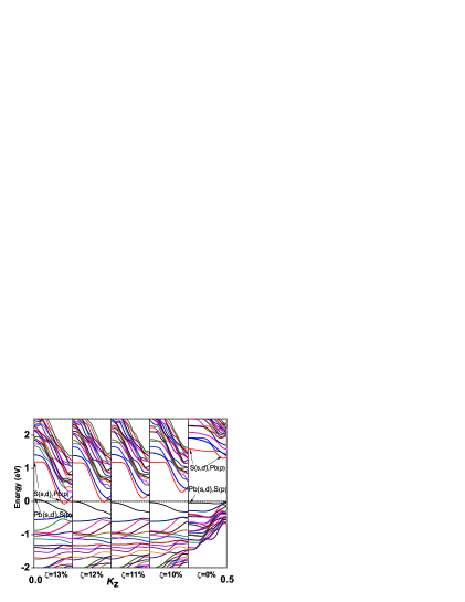
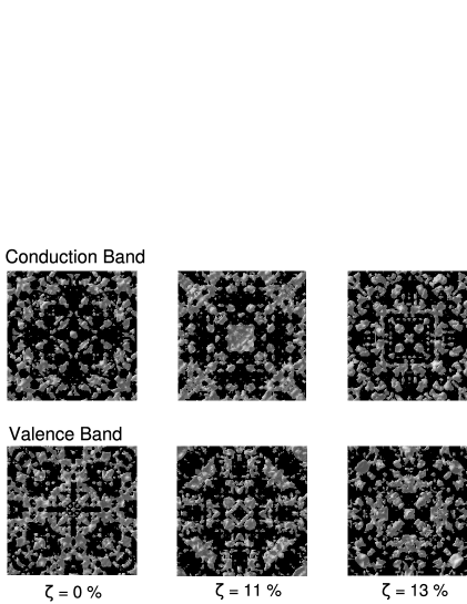
Now we turn our discussions toward the strain induced phase transition of the nanowire. To replicate the effect of radial pressure on the nanowire, we have applied uniform compressive radial strain on a representative NW of diameter 1.98 nm. The NW is allowed to relax in the [200] growth direction under radial strain. The radial strain, , is defined as: , where ; and are the radii of the nanowire with and without the radial strain respectively. The energy band diagrams under different are presented in Fig. 3(a). One can clearly notice the semiconducting to metallic phase transition at . The conduction band, which has a contribution from the excited 3d orbital of S, is found to be more sensitive to the compressive radial strain (CS) with the CBM shifting towards and eventually crossing the Fermi energy with increasing CS. The contribution from the 3d orbital of S at the CBM develops a bonding character in the part of the CB wavefunction resulting in the reduction of its energy under CS. A similar effect of shifting the conduction band under compressive strain is noted in bulk Si strain . The valence band, which is almost dispersionless, develops 0.4 eV dispersion width under compressive radial strain. We have also plotted the wavefunction for the valence and conduction bands at the -point for three different s in Fig. 3(b). A distinct change in the wavefunction due to the change in the hybridization strength between Pb and S under CS is clearly evident from Fig. 3(b). For the NW with d 1.17 nm, the semiconducting to metallic phase transition occurs at about =13 .
To calculate the amount of pressure required for the phase transition, we have plotted the relative deformation potential energy (E ) as a function of in Fig. 4 for the NW of diameter 1.98 nm. The excellent parabolic behavior of E from Fig. 4 allows us to use Hooke’s law to determine the radial Young’s modulus, , which is defined as: . is the length of the unit cell (0.6 nm) at . From the second derivative of the deformation potential E, we have calculated the as 1.9692 eV. Subsequently, the is obtained by using the undeformed radius =0.988 nm. The is found to be 857 GPa. To calculate the amount of pressure () required for the semiconducting to metallic phase transition (), we follow the simple relation that yields 102.8 GPa for the value of P. For the NW of d 1.17 nm, using the same , the P is found to be 111.4 GPa. These values are found to be higher than the reported pressure (3 GPa) for the phase transition estimated using the bulk modulus (127 GPa) of PbS prb . The substantial difference between experiment and theory can be attributed to the lower bulk modulus value prb used to estimate in the experiment. The use of the bulk modulus 127 GPa for prb in our calculation would yield =15.2 GPa for d 1.98 nm, and = 16.5 GPa for d 1.17 nm. These are about five times greater than the experimentally obtained . In addition, the calculation reported here is for uniform, pristine, and defect free PbS NWs, unlike the experimental case, where the PbS NWs are grown within the Na-4 Mica channels in different directions.
It is well known that the energy bandgap obtained from the ground state Kohn-Sham approach does not represent the actual quasiparticle gap measured in the experiment. Thus, it is important to discuss whether the many-body correlation effect, which has been found to be significant for small diameter NW, affects the obtained from GGA based DFT. It has been shown in Si-nanowire that the energy gap obtained using local density approximation (LDA) is significantly smaller than the observed value, which can be corrected by using self-energy correction within the GW approximation prl3 . However, a recent Configuration Interaction (CI) based study in Si nanocrystal suggests that excited state correction method does not make notable difference as compared to the GGA based DFT Nayak . In addition, numerous studies have also confirmed the usefulness of DFT in predicting the trend of energy band gap in nanowires Singh ; strain ; modification . Thus, the trends in that we have observed in PbS nanowire is not expected to change.

IV SUMMARY
In summary, using the density functional approach we have probed for the first time the variation of energy band gap in PbS nanowire with its diameter. We are able to tune the of the PbS nanowire from 0.955 eV to 1.524 eV by varying the diameter from 3.64 nm to 1.17 nm. This is substantially higher than the near infrared direct band gap of 0.41 eV observed for the bulk PbS. The compressive radial strain on the NWs is found to have a significant effect on their electronic properties. A semiconducting to metallic phase transition occurs at = 12 for a representative NW of d 1.98 nm. In addition, we have also observed the strained NW to have an indirect band gap behavior in contrast to the near direct band gap property of the NW. The conduction band of the NW, which has a significant contribution from the excited 3d-orbital of S, is found to be more sensitive to the compressive radial strain. The contribution from the 3d-orbital of S at the conduction band minimum develops a bonding characteristic in the part of the CB wavefuntion, resulting in an energy reduction under CS with the CBM shifting towards and eventually crossing the Fermi energy. Thus, unambiguously, we have identified that the observed phase transition in the recent experiment is due to the CS. The tuning of the electronic structure and hence the bandgap in PbS NWs by varying the diameter of the NWs as well as the external strain on the NWs opens up a new route for their potential applications in nano electronics, optical switches, and solar cells.
ACKNOWLEDGEMENT
We thank Prof. Max Seel for very helpful discussions during this work. RP acknowledges partial support from NSF.
References
- (1) Yu Huang, Xiangfeng Duan, Yi Cui, Lincoln J. Lauhon, Kyoung-Ha Kim, Charles M. Lieber, Science 294, 1313 (2001).
- (2) Yi Cui, Zhaohui Zhong, Deli Wang, Wayne U. Wang, and Charles M. Lieber, Nano Lett. 3, 149 (2003).
- (3) Nicholas A. Melosh, Akram Boukai, Frederic Diana, Brian Gerardot, Antonio Badolato, Pierre M. Petroff, James R. Heath, Science 300, 112 (2003).
- (4) Fernando Patolsky, Gengfeng Zheng, Oliver Hayden, Melike Lakadamyali, Xiaowei Zhuang and Charles M. Lieber, Proceedings of the National Academy of Sciences, U.S.A, 101 14017 (2004).
- (5) Yi Cui, Qingqiao Wei, Hongkun Park, Charles M. Lieber, Science 293, 1289 (2001).
- (6) Eric Stern, James F. Klemic, David A. Routenberg, Pauline N. Wyrembak, Daniel B. Turner-Evans, Andrew D. Hamilton, David A. LaVan, Tarek M. Fahmy, Mark A. Reed, Nature, 445, 519 (2007).
- (7) V. L. Colvin, M. C. Schlamp, and A. P. Alivisatos, Nature 370, 354 (1994).
- (8) Wanli Ma, Joseph M. Luther, Haimei Zheng, Yue Wu, A. Paul Alivisatos, Nano Lett. published online on 12 March 2009.
- (9) Matt Law, Matthew C. Beard, Sukgeun Choi, Joseph M. Luther, Mark C. Hanna, and Arthur J. Nozik, Nano Lett. 8, 3904 (2008).
- (10) Robert Plass, Serge Pelet, Jessica Krueger, Michael Gratzel, Udo Bach, J.Phys. Chem B 106, 7578 (2002).
- (11) Israel Patla, Somobrata Acharya, Leila Zeiri, Jacob Israelachvili, Shlomo Efrima, and Yuval Golan, NanoLett. 7, 1459, (2007).
- (12) P. K. Mukherjee, K. Chatterjee, and D. Chakravorty. Phy. Rev B 73, 035414 (2006).
- (13) Feng Gao, Qingyi Lu, Xiaoying Liu, Yushan Yan, and Dongyuan Zhao, Nano Lett. 1, 743 (2001).
- (14) Serdar Ogut, James R. Chelikowsky, Steven G. Louie, Phy. Rev. lett. 79, 1770 (1997).
- (15) Zhigang Wu, J. B. Neaton, and Jeffrey C. Grossman, Phy. Rev Lett. 100, 246804 (2008).
- (16) Heng Yu, Jinbo Li, Richard A. Loomis, Lin-Wang Wang, William E. Buhro, Nature Materials, 2, 517 (2003).
- (17) Q. Wang, Q. Sun, P. Jena, Y. Kawazeo, Nano Lett. 5, 1587 (2005).
- (18) Vincent Meunier et. al., Nano Lett. published online on 18 March, 2009.
- (19) Wenjie Liang, Allon I. Hochbuam, Melissa Fardy, Oded Rabin, Minjuan Zhang, Peidong Yang, Nano Lett. published online on 24 March 2009.
- (20) Indika U. Arachchige, Mercouri G. kanatzidis, Nano Lett. published online on 24 March 2009.
- (21) Z. Zanolli, M-E Pistol, L E Frogberg, L Samuelson, J. Phys. Condens. Matter 19, 295219 (2007).
- (22) G. Nimtz and B. Schlicht, Narrow-Gap Semiconductors Springer-Verlag, New York, (1985).
- (23) Matthew J. Bierman, Y. K. Albert Lau, and Song Jin, Nano Lett. 7, 2907 (2007).
- (24) Vienna ab initio Simulation Package, Technische Universität Wien, 1999; G. Kresse and J. Furthmüller, Phys. Rev. B 54, 11169 (1996).
- (25) Ki-Ha Hong, Jongseob Kim, Sung-Hoon Lee, and Jai Kwang Shin, Nano Lett. 8, 1355 (2008).
- (26) Xinyuan Zhao, C. M. Wie, L. Yang, M. Y. Chou, Phys. Rev. Lett. 92, 236805 (2004).
- (27) X.-H. Peng, S. Ganti, A. Alizadeh, P. Sharma, S. K. Kumar, S. K. Nayak Phys. Rev. B 2006, 74, 035339
- (28) Abhishek Kumar Singh, Vijay Kumar, Ryunosuke Note, Yoshiyuki Kawazoe, Nano Lett. 6, 920 (2006).
- (29) Michael Nolan, Sean O’Callaghan, Giorgos Fagas, James C. Greer, Nano Lett. 7, 34 (2007).