Thermoelectrical manipulation of nano-magnets
Abstract
We investigate the interplay between the thermodynamic properties and spin-dependent transport in a mesoscopic device based on a magnetic multilayer (F/f/F), in which two strongly ferromagnetic layers (F) are exchange-coupled through a weakly ferromagnetic spacer (f) with the Curie temperature in the vicinity of room temperature. We show theoretically that the Joule heating produced by the spin-dependent current allows a spin-thermo-electronic control of the ferromagnetic-to-paramagnetic (f/N) transition in the spacer and, thereby, of the relative orientation of the outer F-layers in the device (spin-thermo-electric manipulation of nanomagnets). Supporting experimental evidence of such thermally controlled switching from parallel to antiparallel magnetization orientations in F/f(N)/F sandwiches is presented. Furthermore, we show theoretically that local Joule heating due to a high concentration of current in a magnetic point contact or a nanopillar can be used to reversibly drive the weakly ferromagnetic spacer through its Curie point and thereby exchange couple and decouple the two strongly ferromagnetic F-layers. For the devices designed to have an antiparallel ground state above the Curie point of the spacer, the associated spin-thermionic parallel-to-antiparallel switching causes magneto-resistance oscillations whose frequency can be controlled by proper biasing from essentially DC to GHz. We discuss in detail an experimental realization of a device that can operate as a thermo-magneto-resistive switch or oscillator.
I Introduction
The problem of how to manipulate magnetic states on the nanometer scale is central to applied magneto-electronics. The torque effect Slonczewski ; Berger , which is based on the exchange interaction between spin-polarized electrons injected into a ferromagnet and its magnetization, is one of the key phenomena leading to current-induced magnetic switching. Current-induced precession and switching of the orientation of magnetic moments due to this effect have been observed in many experiments Tsoi1 ; Tsoi2 ; Myers ; Katine ; Kiselev ; Rippard ; Beech ; Prejbeanu ; Jianguo ; Dieny .
Current-induced switching is, however, limited by the necessity to work with high current densities. A natural solution to this problem is to use electrical point contacts (PCs). Here the current density is high only near the PC, where it can reachYanson ; Versluijs values A/cm2. Since almost all the voltage drop occurs over the PC the characteristic energy transferred to the electronic system is comparable to the exchange energy in magnetic materials if the bias voltage V, which is easily reached in experiments. At the same time the energy transfer leads to local heating of the PC region, where the local temperature can be accurately controlled by the bias voltage.
Electrical manipulation of nanomagnetic conductors by such controlled Joule heating of a PC is a new principle for current-induced magnetic switching. In this paper we discuss one possible implementation of this principle by considering a thermoelectrical magnetic switching effect. The effect is caused by a non-linear interaction between spin-dependent electron transport and the magnetic sub-system of the conductor due to the Joule heating effect. We predict that a magnetic PC with a particular design can provide both voltage-controlled fast switching and smooth changes of the magnetization direction in nanometer-size regions of the magnetic material. We also predict temporal oscillations of the magnetization direction (accompanied by electrical oscillations) under an applied DC voltage. These phenomena are potentially useful for microelectronic applications such as memory devices and voltage controlled oscillators.
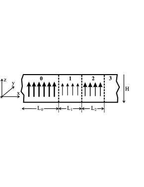
II Equilibrium magnetization distribution
The system under consideration has three ferromagnetic layers coupled to a non-magnetic conductor as sketched in Fig. 1. We assume that the Curie temperature of region 1 is lower than the Curie temperatures of regions 0 and 2; in region 2 there is a magnetic field directed opposite to the magnetization of the region, which can be an external field, the fringing field from layer 0, or a combination of the two. We require this magnetostatic field to be weak enough so that at low temperatures the magnetization of layer 2 is kept parallel to the magnetization of layer 0 due to the exchange interaction between them via region 1 (we assume the magnetization direction of layer 0 to be fixed). In the absence of an external field and if the temperature is above the Curie point, , the spacer of the proposed F/f(N)/F tri-layer is similar to the antiparallel spin-flop ‘free layers’ widely used in memory device applicationsWorledge .
As approaches from below the magnetic moment of layer 1 decreases and the exchange coupling between layers 0 and 2 weakens. This results in an inhomogeneous distribution of the stack magnetization, where the distribution that minimizes the free energy of the system is given by Euler’s equation (see, e.g., Ref. Landau, ):
| (1) |
Here the -axis is perpendicular to the layer planes of the stack, the -axis is directed along the magnetization direction in region 0; the magnetization direction depends only on and the vector rotates in-plane (that is in the -plane) Landau ; is the angle between the magnetic moment at point and the -axis (in the -plane) and . In the case under consideration , for and , for ; here , where is the lattice spacing, and are the exchange energies and magnetic moments of regions 1 and 2; () is a dimensionless measure of the anisotropy energy of region 1 (region 2); is the Boltzmann constant. Below we assume the lengths of regions 1 and 2 to be shorter than the domain wall lengths in these regions .
In order to find the magnetization distribution inside the stack one may solve Eq. (1) in regions 1 and 2 to get and , respectively, and then match these solutions at the magnetization interface . Integrating Eq. (1) with respect to in the limits one gets the matching condition as follows:
| (2) |
The boundary condition at the ferromagnetic interface between layers 0 and 1 follows from the requirement that the direction of the magnetization in layer 0 is fixed along the -axis (i.e., in this layer):
| (3) |
At the "free" end of the ferromagnetic sample the boundary condition for the magnetization is (see, e.g. Ref. Akhiezer, ), so that
| (4) |
Solving Eq. (1) in regions 1 and 2 under the assumption and with the boundary conditions (2) - (4) one finds the magnetization in region 1 to be inhomogeneous,
| (5) |
while due to the boundary condition (4) the magnetic moments in region 2 are approximately parallel, to within corrections of order , i.e.
| (6) |
where . Using the above boundary conditions one finds that is determined by the equation
| (7) |
where
| (8) |
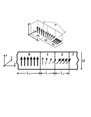
In Eq. (8) and are the magnetic moments of region 1 and 2, respectively; the parameter is the ratio between the magnetic energy and the energy of the stack volume for the inhomogeneous distribution of the magnetization. As the second term inside the brackets in Eq. (6) is negligibly small, the magnetization tilt angle in region 2 becomes independent of position and is simply given as a function of and by Eq. (II).
By inspection of Eq. (II) one finds that it has either one or several roots in the interval depending on the value of the parameter .
At low temperatures the exchange energy prevails, the parameter and Eq. (II) has only one root, . Hence a parallel orientation of all magnetic moments in the stack is thermodynamically stable. However, at temperature for which , two new roots appear. The parallel magnetization corresponding to is now unstable phase and the direction of the magnetization in region 2 tilts as indicated in Fig. 2. Using Eq.(8) one finds the critical temperature of this orientation transition to be equal to
| (9) |
The tilt increases further with until at the exchange coupling between layers 0 and 2 vanishes and their magnetic moments become antiparallel.
Thermally assisted exchange decoupling in F/f/F multilayers
To demonstrate the properties of the tri-layer material system proposed above we have suitably alloyed Ni and Cu to obtain a spacer with a just higher than room temperature (RT). The alloying was done by co-sputtering Ni and Cu at room temperature and base pressure torr on to a 90x10 mm long Si substrate in such a way as to obtain a variation in the concentration of Ni and Cu along the substrate. By cutting the substrate into smaller samples along the compositional gradient, a series of samples were obtained, each having a different Curie temperature.
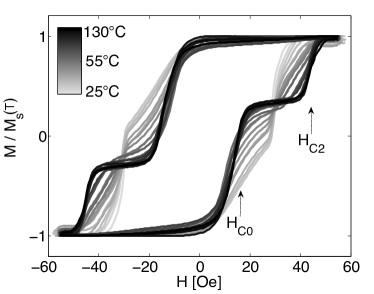
One of the multi-layer compositions chosen was NiFe 8/CoFe 2/NiCu 30/ CoFe 5 where the NiFe layer is used to lower the coercive field of the bottom layer (HC0) in order to separate it from the switching of the top layer (HC2). A magnetometer equipped with a sample heater was used to measure the magnetization loop as the temperature was varied between C and C. The results for a Ni concentration of 70% are shown in Fig. 3. The strongly ferromagnetic outer layers are essentially exchange-decoupled at C (F/Paramagnetic/F state), as evidenced by the two distinct magnetization transitions at approximately 15 and 45 Oe in Fig. 3. As the temperature is reduced to RT, the switching field of the soft layer increases and the originally sharp - transition becomes significantly skewed. This confirms the theoretical result, expressed by Eqs. (5) and (6) for , that the magnetic state of the sandwich is of the spring-ferromagnet type spring_mag . The lowering of temperature leads at the same time to a lower switching field of the magnetically hard layer, which is due to the stronger effective magnetic torque on the top layer in the coupled F0/f/F2 state. This thermally-controlled interlayer exchange coupling is perfectly reversible on thermal cycling within the given temperature range.
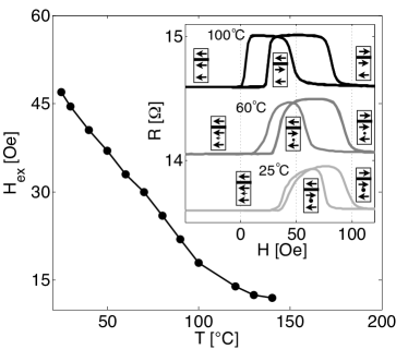
We further demonstrate an exchange-biased magnetic tri-layer of the generic composition AF/F0/f/F2, where the spacer separating the outer ferromagnetic layers (F) is a low-Curie temperature diluted ferromagnetic alloy (f) and one of the F0 layers is exchange-pinned by an antiferromagnet (AF). In addition to the tri-layer a Cu spacer and a reference layer, pinned by an AF, have been added on top of the stack in order to measure the current-in-plane giant magnetoresistance (GMR). The specific stack composition chosen was Si/SiO2/NiFe 3/MnIr 15/CoFe 2/ Ni70Cu30 30/CoFe 2/NiFe 10/CoFe 2 /Cu 7/CoFe 4/NiFe 3/MnIr 15/Ta 5 [nm]. The sample was deposited at room temperature in a magnetic field of 350 Oe, then annealed at 300∘C for 20 minutes, and field cooled to RT in Oe. The NiCu spacer was co-sputtered while rotating the substrate holder, such that the final concentration was 70 Ni and 30 Cu having the suitably above RT. Fig. 4 shows how the interlayer exchange field Hex of this sample varies with temperature. Hex shown in the main panel of Fig. 4 is defined as the mid point switching field of the soft F2-layer (, , and Oe for C, C, and C, respectively; see inset), which reflects the strength of the interlayer exchange coupling through the spacer undergoing a ferromagnetic-paramagnetic transition in this temperature range. To explain why this is so, we need to consider the difference in effective magnetic thickness between the top and bottom pinned ferromagnetic layers. The effective magnetic thickness for the bottom pinned CoFe/NiCu/CoFe/NiFe/CoFe layers is approximately three times larger than for the top pinned CoFe/NiFe. From the inset to Fig 4, the temperature variation of the exchange pinning for the top pinned CoFe/NiFe is 20 Oe or 0.3 Oe/K. If we were to assume that the bottom pinned CoFe/NiCu/CoFe/NiFe/CoFe layers are coupled and reverse as one layer, and that the variation in exchange field is caused solely by the weakening pinning at the bottom MnIr interface, then we would expect an exchange field three times smaller than for the top pinned CoFe/NiFe. With a three times smaller exchange field at RT the expected temperature variation would be 7 Oe or 0.1 Oe/K, which clearly is much lower than the observed change of 25 Oe (from 45 Oe to 20 Oe) and therefore the measured de-pinning of the switching layer is predominantly due to a softening of the exchange spring.
We have separately measured the strength of the exchange pinning at the bottom MnIr surface. For CoFe ferromagnetic layers 2-4 nm thick, the pinning strength at RT is 500 Oe or more. At 130 C, at which the spacer is paramagnetic and fully decoupled from the underlying MnIr/CoFe bilayer, the pinning strength is still above 100 Oe. We therefore conclude that the dominating effect in question is the weakening exchange spring in the spacer. This demonstrates the principle of the thermionic spin-valve proposed, where the P to AP switching is controlled by temperature. The AF-pinned implementation of the spin-thermionic valve presented should be highly relevant for application.
As is obvious from the above analysis the dependence of the magnetization direction on temperature allows electrical manipulations of it by Joule heating with an applied current flowing through the stack. In the next section we find connection between the magnetization direction and the current-voltage characteristics (IVC) of such a spin-thermionic valve.
III Thermoelectric manipulation of the magnetization direction.
III.1 Current-voltage characteristics of the stack under Joule heating.
If the stack is Joule heated by a current its temperature is determined by the heat-balance condition
| (10) |
and Eq. (II), which determines the temperature dependence of . Here is the heat flux from the stack and is the stack resistance. In the vicinity of the Curie temperature Eq. (II) can be re-written as
| (13) |
(here is defined in Eq.(9)).
Equations (10) and (13) define the current-voltage characteristics (IVC) of the stack, , , in a parametric form which can be re-written as
| (14) |
The parameter is defined in the interval ,
and in order to derive Eq. (14) we used the expansion [].
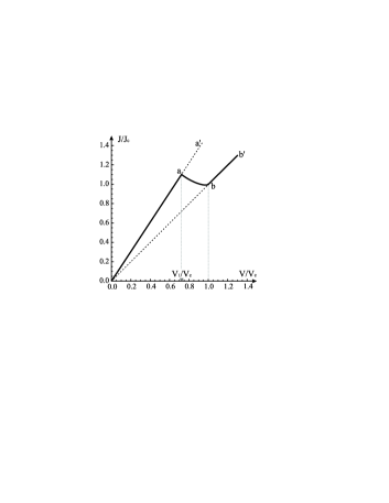
It follows from Section II that the stack resistance is in the entire temperature range and in the range . This implies that the IVC branches and are linear for, respectively,
| (15) |
( in Fig. 5) and
| (16) |
( in Fig. 5). If the stack temperature is , and the direction of the magnetization in region 2 changes with a change of ; hence the IVC is non-linear there. Below we find the conditions under which this branch of the IVC has a negative differential conductance.
Differentiating Eq. (14) with respect to one finds
| (17) |
where means the derivative of the bracketed quantity with respect to the angle , and is found from the second equation in Eq. (14). From this result it follows that the differential conductance is negative if
For a stack resistance of the form
| (18) |
where
| (19) |
one finds that the differential conductance if
| (20) |
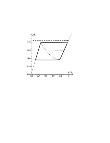
Hence the IVC of the stack is N-shaped as shown in Fig. 5.
We note here that the modulus of the negative differential conductance may be large even in the case that the magnetoresistance is small. Using Eq.(15) at one finds the differential conductance as
| (21) |
which is negative provided , the modulus of being of the order of .
Here and below we consider the case that the electric current flowing through the sample is lower than the torque critical current and hence the torque effect is absent torquecurrent
As the IVC curve is N-shaped the thermoelectrical manipulation of the relative orientation of layers 0 and 2 may be of two different types depending on the ratio between the resistance of the stack and resistance of the circuit in which it is incorporated
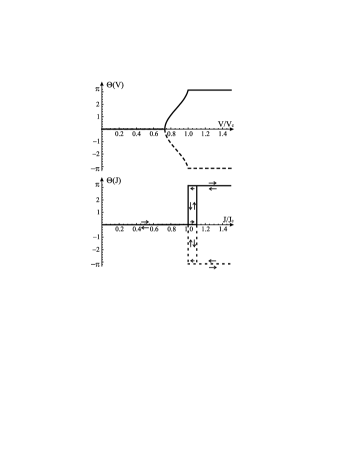
In the voltage-bias regime which corresponds to the case that the resistance of the stack is much larger than resistance of the rest of the circuit, the voltage drop across the stack preserves the given value which is approximately equal to the bias voltage and hence there is only one value of the current (one point on the IVC) corresponding to the bias voltage (see Fig.5) In this case the relative orientation of the magnetization of layers 0 and 2 can be changed smoothly from being parallel to anti-parallel by varying the bias voltage through the interval . This corresponds to moving along the branch of the IVC. The dependence of the magnetization direction on the voltage drop across the stack is shown in Fig. 6.
In the current-bias regime, on the other hand, which corresponds to the case that the resistance of the stack is much smaller than the resistance of the circuit, the current in the circuit is kept at a given value which is mainly determined by the bias voltage and the circuit resistance (being nearly independent of the stack resistance). As this takes place, the voltage drop across the stack differs from the bias voltage , being determined by the equation . As the IVC is N-shaped, the stack may now be in a bistable state: if the current is between points and there are three possible values of the voltage drop across the stack at one fixed value of the current (see Fig. 5). The states of the stack with the lowest and the highest voltages across it are stable while the state of the stack with the middle value of the voltage drop is unstable. Therefore, a change of the current results in a hysteresis loop as shown in Fig. 6: an increase of the current along the branch of the IVC leaves the magnetization directions in the stack parallel () up to point , where the voltage drop across the stack jumps to the right branch , the jump being accompanied by a fast switching of the stack magnetization from the parallel to the antiparallel orientation (). A decrease of the current along the IVC branch keeps the stack magnetization antiparallel up to point , where the voltage jumps to the left branch of the IVC and the magnetization of the stack comes back to the parallel orientation ().
In the next Section we will show that this scenario for a thermal-electrical manipulation of the magnetization direction is valid for small values of the inductance in the electrical circuit. If the inductance exceeds some critical value the above steady state solution becomes unstable and spontaneous oscillations appear in the values of the current, voltage drop across the stack, temperature, and direction of the magnetization.
III.2 Self-excited electrical, thermal and directional magnetic oscillations.
III.2.1 Current perpendicular to layer planes (CPP)
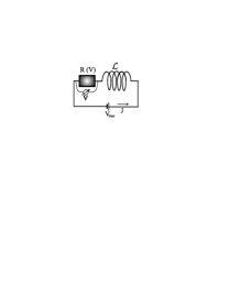
Consider now a situation in the bias voltage regime where the magnetic stack under investigation is connected in series with an inductance and biased by a DC voltage , as described by the equivalent circuit in Fig. 7. The thermal and electrical processes in this system are governed by the set of equations
| (22) |
where is the heat capacity. The relaxation of the magnetic moment to its thermodynamically equilibrium direction is assumed to be the fastest process in the problem, which implies that the magnetization direction corresponds to the equilibrium state of the stack at the given temperature . In other words, the tilt angle, , adiabatically follows the time-evolution of the temperature and hence its temperature dependence is given by Eq. (II).
A time dependent variation of the temperature is accompanied by a variation of the magnetization angle and hence by a change in the voltage drop across the stack via the dependence of the magneto-resistance on this angle, .
The system of equations Eq.(22) has one time-independent solution () which is determined by the equations
| (23) |
This solution is identical to the solution of Eqs.(II,10) that determines the N-shaped IVC shown in Fig.5 with a change and .
In order to investigate the stability of this time-independent solution we write the temperature, current and the angle as a sum of two terms,
| (24) |
where , and each is a small correction. Inserting Eq.(24) into Eq.(22) and Eq. (II) one easily finds that the time-independent solution Eq.(23) is always stable at any value of the inductance if the bias voltage corresponds to a branch of the IVC with a positive differential resistance (branches 0-a and b-b’ in Fig.5). If the bias voltage corresponds to the branch with a negative differential resistance (, see Fig.5) the solution of the set of linearized equations is , and where , and are any initial values close to the steady-state of the system, and
| (25) |
where
| (26) |
and , is the differential resistance.
As is seen from Eq.(25) the steady-state solution Eq.(23) is stable only if the inductance ; if the inductance exceeds the critical value Eq.(26) the system looses its stability and a limit cycle appears in the plane (see, e.g., Hilborn ). This corresponds to the appearance of self-excited, non-linear and periodic temporal oscillations of the temperature and the current , which are accompanied by oscillations of the voltage drop across the stack and the the magnetization direction . For the case that the system executes nearly harmonic oscillations around the steady state (see Eq.(24)) with the frequency , that is the temperature , the current , the magnetization direction and the voltage drop across the stack execute a periodic motion with the frequency
| (27) |
With a further increase of the inductance the size of the limit cycle grows, the amplitude of the oscillations increases and the oscillations become anharmonic, the period of the oscillations therewith decreases with an increase of the inductance .
In order to investigate the time evolution of the voltage drop across the stack and the current in more details it is convenient to introduce an auxiliary voltage drop and a current related to each other through Eqs. (10) and (13). Hence we define
| (28) |
where . Comparing these expressions with Eq. (10) one sees that at any moment Eq. (28) gives the stationary IVC of the stack, , defined by Eq. (14) (changing and ), see Fig. (5).
Differentiating with respect to and using Eqs. (22) and (28) one finds that the dynamical evolution of the system is governed by the equations
| (29) |
where
As follows from the second equation in Eq. (28), at any moment the voltage drop over the stack is coupled with by the following relation:
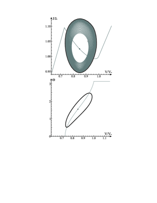
The coupled equations (22) have only one steady-state solution where is the IVC shown in Fig.5 (see Eqs. (28). However, in the interval this solution is unstable with respect to small perturbations if . As a result periodic oscillations of the current and appear spontaneously, with , eventually reaching a limit cycle. The limiting cycle in the - plane is shown in Fig. 8. The stack temperature , the magnetization direction , follow these electrical oscillations adiabatically according to the relations (here ) and (see Eq. (II)) as shown in Fig. 9.
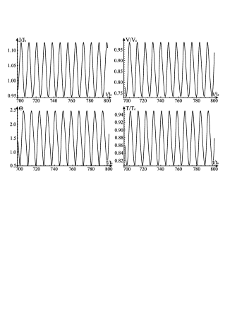
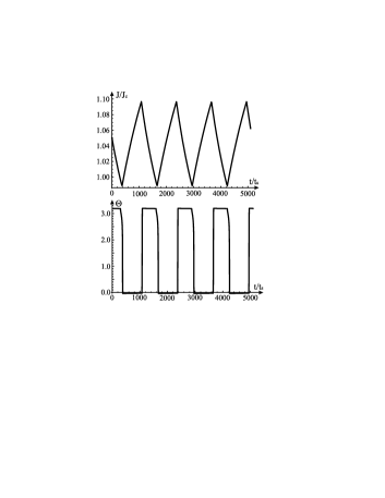
The character of the oscillations changes drastically in the limit . In this case the current and the voltage slowly move along the branches and of the IVC at the rate , quickly switching between these branches at the points and with the rate (see Fig. 10). Therefore, in this case the stack periodically switches between the parallel and antiparallel magnetic states (see Fig. 11).
III.2.2 Current in the layer planes (CIP).
If the electric current flows in the plane of the layers (CIP) of the stack the torque effect is insufficient or absent Slonczewski ; Ralph while the magneto-thermal-electric oscillations under consideration may take place. In this case the total current flowing through the cross-section of the layers may be presented as
| (30) |
where and are the magneto-resistance and the angle-independent resistance of the stack in the CIP set of the experiment.
In a CIP configuration the stack is Joule heated by both the angle-dependent and the angle-independent currents and hence Eq.(10) should be re-written as follows:
| (31) |
where
| (32) |
Using Eq.(17) and Eq.(30) one finds that the presence of the angle-independent current in the stack modifies the condition of the negative differential conductance : it is negative if
| (33) |
As is seen from here, an IVC with a negative differential resistance is possible if (see Eq.[19] for definitions of and ).
The time evolution of the system is described by the set of equations Eq.(22) in which one needs to change and . Therefore, under this change, the temporal evolution of the system in a CIP configuration is the same as when the current flows perpendicular to the stack layers: if the bias voltage corresponds to the negative differential conductance and the inductance exceeds the critical value
| (34) |
where , self-excited oscillations of the current , voltage drop over the stack , the temperature and the angle arise in the system, the maximal frequency of which being
| (35) |
if
Below we present estimations of the critical inductance and the oscillation frequency which are valid for both the above mentioned CPP and CIP configurations of the experiment.
Using equations Eq.(23) and Eq.(26) one may estimate the order of magnitude of the critical inductance and the oscillation frequency as and where is the heat capacity per unit volume, is the resistivity, and is a characteristic size of the stack. For point contact devices with typical values of , K, cm, and assuming that cooling of the device can provide the sample temperature one finds the characteristic values of the critical inductance and the oscillation frequency as and
IV Conclusions.
The experimental implementation of the new principle proposed in this paper for the electrical manipulation of nanomagnetic conductors by means of a controlled Joule heating of a point contact appears to be quite feasible. This conclusion is supported both by theoretical considerations and preliminary experimental results, as discussed in the main body of the paper. Hence we expect the new spin-thermo-electronic oscillators that we propose to be realizable in the laboratory. We envision F0/f/F2 valves where two strongly ferromagnetic regions ( K) are connected through a weakly ferromagnetic spacer ( K). The Curie temperature of the spacer would be variable on the scale of room temperature, chosen during fabrication to optimize the device performance. For example, doping Ni-Fe with of Mo brings the from K to 300-400 K. Alternatively, alloying Ni with Cu yields a spacer with a just above Room Temperature (at RT or below RT, if needed). If a sufficient current density is created in the nano-tri-layer to raise the temperature to just above the of the spacer, the magnetic subsystem undergoes a transition from the F0/f/F2 state to an F0/N/F2 state, the latter being similar to conventional spin-valves (N for nonmagnetic, paramagnetic in this case). Such a transition should result in a large resistance change, of the same magnitude as the “giant magnetoresistance" (GMR) for the particular material composition of the valve.
Local heating (up to 1000 K over 10-50 nm) can readily be produced using, e.g., point contacts in the thermal regime, with very modest global circuit currents and essentially no global heating Yanson . Heat is known to propagate through nm-sized objects on the ns time scale, which can be scaled with size to the sub-ns regime. When voltage-biased to generate a temperature near , such a F0/f/F2 device would oscillate between the two magnetic states, resulting in current oscillations of a frequency that can be tuned by means of connecting a variable inductance in series with the device. Spin rotation frequencies may be tuned from the GHz-range down to quasi-DC (or DC as soon as the inductance is smaller than the critical value). For F0/f/F2 structures geometrically designed in the style of the spin-flop free layer of today’s magnetoresistive random access memory (MRAM), the dipolar coupling between the two strongly ferromagnetic layers would make the anti-parallel state ( ) the magnetic ground state above . The thermal transition in the f-layer would then drive a full 180-degree spin-flop of the valve. The proposed spin-thermo-electronic valve can be implemented in CPP as well as CIP geometry, which should make it possible to achieve MR signals of 10.
In conclusion, we have shown that Joule heating of the magnetic stack sketched in Fig. 1 allows the relative orientation of the magnetization of the two ferromagnetic layers 0 and 2 to be electrically manipulated. Based on this principle, we have proposed a novel spin-thermo-electronic oscillator concept and discussed how it can be implemented experimentally.
Acknowledgement. Financial support from the Swedish VR and SSF, the European Commission (FP7-ICT-2007-C; proj no 225955 STELE) and the Korean WCU programme funded by MEST through KOSEF (R31-2008-000-10057-0) is gratefully acknowledged.
References
- (1) J. C. Slonczewski, J. Magn. Magn. Mater. 159, L1 (1996); ibid. 195, L261 (1999).
- (2) L. Berger, Phys. Rev. B 54, 9353 (1996).
- (3) M. Tsoi, A . G. M. Jansen, J. Bass, W.-C. Chiang, M. Seck, V. Tso, and P. Wyder, Phys. Rev. Lett. 80, 4281 (1998).
- (4) M. Tsoi, A. G. M. Jansen, J. Bass, W.-C. Chiang, V. Tsoi, and P. Wyder, Nature (London), 406, 46 (2000).
- (5) E. B. Myers, D. C. Ralph, J. A. Katine, R. N. Louie, and R. A. Buhrman Science 285, 867 (1999).
- (6) J. A. Katine, F. J. Albert, R. A. Buhrman, E. B. Myers, and D. C. Ralph, Phys. Rev. Lett. 84, 3149 (2000).
- (7) S. I. Kiselev, J. C. Sankey, I. N. Krivorotov, N. C. Emley, R. J. Schoelkopf, R. A. Buhrman, and D. C. Ralph, Nature (London) 425, 380 (2003).
- (8) W. H. Rippard, M. R. Pufall, and T. J. Silva, Appl. Phys. Lett. 82, 1260 (2003).
- (9) R. S. Beech, J. A. Anderson, A. V. Pohm, and J. M. Daughton, J. Appl. Phys. 87, 6403 (2000).
- (10) I. L. Prejbeanu, W. Kula, K. Ounadjela, R. C. Sousa, O. Redon, B. Dieny, J.-P. Nozieres, IEEE Trans. Magn. 40, 2625 (2004)
- (11) Jianguo Wang and P. P. Freitas, Appl. Phys. Lett. 84, 945 (2004).
- (12) M. Kerekes, R. C. Sousa, I. L. Prejbeanu, O. Redon, U. Ebels, C. Baraduc, B. Dieny, J.-P. Nozieres, P. P. Freitas, and P. Xavier, J. Appl. Phys. 97, 10P501 (2005).
- (13) A. V. Khotkevich and I. K. Yanson, Atlas of Point Contact Spectra of Electron-Phonon Interactions in Metals, Kluwer Academic Publishers, Boston/Dordrecht/London (1995).
- (14) J. J. Versluijs, M. A. Bari, and M. D. Coey, Phys. Rev. Lett. 87, 026601 (2001).
- (15) V. Korenivski and D. C. Worledge, Appl. Phys. Lett. 86, 252506 (2005).
- (16) L. D. Landau, E. M. Lifshits, and L. P. Pitaevski, Electrodynemics of Continuous Media, §43, Butterworth-Heinemann, Oxford, Pergamon Press 1998.
- (17) A. I. Akhiezer, V. C. Bar’yakhtar, S. V. Peletminskii, Spin Waves, §5.4, p.42, North-Holland Publishing Company - Amsterdam John Wiley & Sons, INC. - New York, 1968.
- (18) The temperature is the critical temperature of an orientational phase transition that arises in the stack when the magnetic energy and the energy of the stack volume for the inhomogeneous distribution of the magnetization become equal. This phase transition is analogous to orientational phase transitions in anisotropic ferromagnets based on the dependence of the magnetic anisotropy constant on temperature, H. Horner and C. M. Varma, Phys. Rev. Lett. 20, 845 (1968), see also, e.g., Ref. Landau, , §46 "Orientation transitions".
- (19) J. E. Davies, O. Hellwig, E. E. Fullerton, J. S. Jiang, S. D. Bader, G. T. Zimanyi, and K. Liu, Appl. Phys. Lett. 86, 262503 (2005).
- (20) Typical densities of critical currents needed for the torque effect in point-contact devices are for the current perpendicular to the layers (CPP) Ralph
- (21) D.C. Ralph, and M.D. Stiles, Journal of Magnetism and Magnetic Materials, 320, 1190 (2008).
- (22) Robert C. Hilborn, Chaos and Nonlinear Dynemics, p. 112 (Oxford, University Press, 2000).