Topological Frustration in Graphene Nanoflakes:
Magnetic Order and Spin Logic Devices
Abstract
Magnetic order in graphene-related structures can arise from size effects or from topological frustration. We introduce a rigorous classification scheme for the types of finite graphene structures (nano-flakes) which lead to large net spin or to antiferromagnetic coupling between groups of electron spins. Based on this scheme, we propose specific examples of structures that can serve as the fundamental (NOR and NAND) logic gates for the design of high-density ultra-fast spintronic devices. We demonstrate, using ab initio electronic structure calculations, that these gates can in principle operate at room temperature with very low and correctable error rates.
pacs:
75.75.+a, 81.05.Uw, 85.75.-dMagnetism in solids is typically associated with the presence of transition metal elements with electrons. Experimental evidence has recently shown that magnetism can also arise in solids composed of elements with only electrons, as, for example, in bulk proton irradiated graphite Esquinazi03 . Theoretical studies addressing the issue of magnetism in carbon-based materials have focused on point defects Duplock04 ; Yazyev07 ; Palacios08 and reduced dimensionality Son06 ; Yazyev08a ; Ezawa07 ; Fernandez-Rossier07 ; Wang08 ; Bhowmick08 . These works have shown that magnetism can arise in various situations, for example, the antiferromagnetic order across the edges of zigzag-edged graphene nanoribbons Son06 and the large net spin in zigzag-edged triangular graphene nanoflakes Ezawa07 ; Fernandez-Rossier07 ; Wang08 . On the other hand, magnetism from electrons is not new in organic chemistry: high-spin states have been observed in synthesized organic molecules, for example, conjugated polyradicals rajca01 and triangulene derivatives Allinson95 , where all conjugated electrons can not be paired simultaneously. At present, it is not yet clear if the magnetic properties of irradiated bulk graphite and those of high-spin organic molecules have the same origin. Understanding of the magnetic order and its origin in various finite graphene structures is of fundamental importance as well as of practical interest for application in spintronics Wolf01 where carbon based materials have recently demonstrated their potential Hueso07 .
In this letter, we show that a distinct origin of magnetism in finite graphene structures is topological frustration of bonds, which is a generalization of the simple counting rule that governs magnetic order in organic molecules. We use the notion of this topological frustration to derive a rigorous classification scheme for arbitrarily shaped graphene nanoflakes, depending on whether only one or both sublattices of the graphitic structure are frustrated. From this classification scheme we identify which nanoscale structures can give rise to a strong antiferromangetic (AF) coupling and propose a specific example of a structure which can serve as the fundamental (NOR and NAND) spin logic gate. Finally, we employ first-principles electronic structure calculations to show that this type of gate can operate at room temperature, an important prerequisite for the design of realistic, high-density ultra-fast spintronic devices based on graphene.
A graphene nanoflake (GNF) is an arbitrarily shaped finite graphene fragment consisting of hexagonal rings and bounded by a single (non-self-intersecting) topological circuit, where all in-plane dangling -bonds at the edge are assumed passivated. We start the general classification of GNFs with the widely used band Hubbard model, where magnetic correlations are described through the hamiltonian
| (1) |
In the first term, the tight-binding part, the operators () annihilate (create) an electron at site with spin and is the hopping integral between the nearest neighbor sites and . The honeycomb lattice of graphene is bipartite, that is, any pair of bonded nearest neighbor carbon atoms consists of one atom from each of the two interpenetrating sublattices, commonly denoted as and (Fig. 1). The second term of the hamiltonian describes electron-electron interactions via the on-site Coulomb repulsion with the number operator. This interaction may trigger an instability in the low-energy electronic states and produce spin polarized states to minimize the total energy. Zero-energy (non-bonding) states in a half-filled sub-band are particularly prone to become polarized for .
The occurrence of zero-energy eigenstates in the tight-binding hamiltonian for a GNF can be accounted for by a theorem on hexagonal graphs Fajtlowicz05 . The number of such states, called “nullity” (), is determined by the topology of the GNF according to the equation , where and are the maximum numbers of non-adjacent vertices and edges respectively. The latter is also called the maximum matching of the GNF graph and satisfies the relations , where and are the numbers of positive and negative eigenstates respectively. The sum equals to , the total number of carbon atoms in the GNF. When , and all carbon atoms can be connected by a set of non-adjacent pair-wise bonds, which is referred to as “perfect matching” indicating a perfect pairing of all orbitals. Otherwise, , which is the number of sites that are left out by the best possible matching. The inability to simultaneously pair all orbitals is entirely attributed to the topology of the GNF, therefore can be called topological frustration.
In general, GNFs can be classified into two classes according to whether one or both sublattices are topologically frustrated. In class I, at most one of the sublattices is frustrated, which is characterized by , that is, the maximum matching covers all sites of at least one sublattice. This class includes all highly symmetric forms of GNFs as we proved previously Wang08 . The nullity for this class is simply , as illustrated in Fig. 1(a) and 1(b). Balanced sublattices () means zero nullity. In class II, both sublattices are frustrated, characterized by (note ), which means . As a result, the nullity can be finite even for GNFs with balanced sublattices. An example is shown in Fig. 1(c), where the nullity is even though .
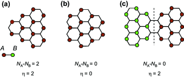
Although graph theory is all that is required to predict the number of singly-occupied orbitals, it is not clear how the electron spins in these orbitals are aligned. Complementary information comes from the Lieb theorem Lieb89 which determines the total spin but not the number of singly-occupied orbitals. The Lieb theorem was proved for any even-numbered bipartite system, where the ground state has a total magnetic moment . Therefore, for class I GNFs, , that is, all spins in singly-occupied orbitals align parallel to each other, consistent with Hund’s rule. This was confirmed experimentally Allinson95 and by first-principles calculations Fernandez-Rossier07 ; Wang08 . For class II GNFs, , indicating the existence of antiferromagnetic (AF) order, and Hund’s rule breaks down. Specifically, for the bowtie shaped GNF shown in Fig. 1(c), the magnetic moments of the left and right triangle must be AF coupled to satisfy the requirement . This is also consistent with the fact that magnetic moments are localized in the two sublattices of graphene favoring AF coupling Yazyev07 ; Brey07 .
Besides topological frustration, AF coupling can also be induced by the polarization of the low-energy states that approach the Fermi level as the system size increases. This is a distinctly different origin of magnetism, for two reasons: first, it can not give rise to net spin; second, the energy of the non-interacting eigenstate is not strictly at the Fermi level, except in infinite systems, and magnetic order appears only if the interaction energy is above a positive threshold or, equivalently, if the system is above a critical size. Examples of this mechanism are graphene nanoribbons Nakada96 and hexagonal graphene nanoflakes Fernandez-Rossier07 .
We next focus on the magnetic coupling induced by topological frustration in class II GNFs and use the bowtie structure of Fig. 1(c) as the simplest representatives. Such structures have a low-spin ground state, involving spins spatially segregated and AF coupled. This open-shell, low-spin feature is not only fundamentally interesting but also may enable practically accessible logic operations. For instance, the simple bowtie structure is a natural NOT gate because flipping the input spins on one side of the bowtie requires the output spins on the other side to flip as well since the spins on the two sides must point in opposite directions as long as the AF order is the ground state. Practically, various means may be used to flip the input spin, including polarized light, local magnetic fields or direct injection of polarized electrons through magnetic materials. Among those, spin injection Wimmer08 appears the most promising, especially when considering the natural integration of GNFs with graphene nanoribbons which have been predicted to exhibit rich spintronic properties including half metallicity Son06 ; Wang08 . The barrier for flipping the output spin is expected to be extremely low () due to the weak spin-orbit coupling in carbon materials Yazyev08a , which is a prerequisite for operation with low energy consumption. In order to achieve both ultra-fast switching and robust operation at reasonable temperatures, it is also important to have the magnetic coupling , the energy difference between the ferromagnetic and antiferromagnetic configurations, be greater than 18 meV, the minimum energy dissipation Landauer61 evaluated at 300 K. In principle, picosecond flipping of electron spins can be achieved with an energy splitting sec meV.
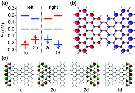
In order to establish whether or not the above conditions can be met, we turn to first-principles electronic structure methods to investigate the energetics of magnetic coupling in detail. Calculations were performed using spin-polarized density functional theory (DFT) as implemented in the SIESTA code SIESTA . The generalized gradient approximation (GGA) exchange-correlation functional Perdew96 was employed together with a double- plus polarization basis set, norm-conserving pseudopotentials Troullier91 and a mesh cutoff of 200 Ry. The different spin configurations were obtained by means of providing appropriate initial guess electron spin densities Yazyev08b ; Convergence . The electronic structure of a representative bowtie GNF is shown in Fig. 2. The nullity of the corresponding graph, , manifests itself as four singly-occupied orbitals. Within the spin-polarized formalism, when spin-spatial symmetry breaking is allowed these four states are split, as shown in Fig. 2(a). The wave functions clearly illustrate the open shell singlet nature of the system: electrons are AF coupled but not paired in the sense that they are spatially segregated, in agreement with previous calculations Pogodin03 on non-kekuléan molecules. The spin coupling here is meV, well beyond the above mentioned thermodynamic threshold.
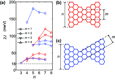
The coupling strength in a bowtie GNF can be further engineered by optimizing its geometry. To explore possibilities, we calculated bowtie nanoflakes of different triangle size and junction width (both measured in units of the graphene lattice constant, nm) for both symmetric and asymmetric geometries, shown in Fig. 3. In either case, there are non-bonding states on each triangularly shaped side of the bowtie GNFs. The calculated coupling magnitude converges quickly with increasing after reaching a maximum value Fig. 3(a). The leveling off is attributed to the size effect which diminishes the minimum energy splitting. Interestingly, for a specific asymmetric configuration, the interaction strengths are as large as meV. In comparison, the AF coupling of quantum dots Agarwal08 and transition metal atoms Hirjibehedin06 suffer from weak maximum coupling strength, about 1 meV and 6 meV respectively, limiting their operation to very low temperatures. With a coupling of 180 meV, a GNF-based spin gate may operate at room temperature with an error rate of , which can be handled by error correction schemes.
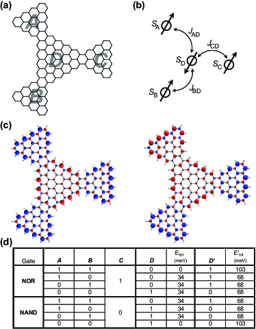
To further illustrate the concept of using Class II GNFs for spin logic processing, we explore a tri-bowtie GNF in which the central triangle is connected to three other surrounding triangles through its vertices, as shown in Fig. 4(a). From graph theory arguments, we expect the number of unpaired spins in the central region to be where () are the widths of the junctions; the peripheral triangles accommodate unpaired spins. The unpaired spins in the central region now depend on the competition of the spins of all the three peripheral regions: they tend to be AF coupled to the majority spins of the peripheral regions so that the total energy is lowered. We can therefore assign the total spins of two of those peripheral regions as operands and and the third as a programming bit ; the spin in the central region is the output. With the spin-up state representing 1 and the spin-down state 0, the above logic is written as
If is 1, the logic reduces to , a NOR gate; if is 0, , a NAND gate; these are the two fundamental gates in Boolean logic, from either one of which all other gates can be constructed. Therefore, the above scheme in principle provides an efficient design, with the spin degree of freedom employed to satisfy in the classic regime all digital logic operations.
Undoubtedly, various engineering issues will have to be addressed before the actual operation of such a device. For instance, the design of the device ground state by coupling to peripheral leads, fan-out, and control of unidirectional logic flow are all open issues. Fabrication of the bowtie structure is another challenge, but recent experiments demonstrated that graphene devices only a few nanometers in size can be sculpted by electron beam or scanning probes and are quite stable Ponomarenko08 ; Tapaszto08 . Meanwhile, we point out that the demands on fabrication are significantly alleviated by the intrinsic defect-tolerability of the spin GNF devices: at least out of carbon atoms can be removed (excluding those atoms at the junction to which the device function is highly sensitive) from the dominant sublattice in an individual triangle of size before the non-bonding states are eliminated and the local magnetic moment quenched. These considerations indicate that the devices based on the proposed design are not beyond the reach of modern nano-scale fabrication methods.
References
- (1) P. Esquinazi et al., Phys. Rev. Lett. 91, 227201 (2003); H. Ohldag et al., Phys. Rev. Lett. 98, 187204 (2007).
- (2) E. J. Duplock, M. Scheffler, and P. J. D. Lindan, Phys. Rev. Lett. 92, 225502 (2004).
- (3) O. V. Yazyev and L. Helm, Phys. Rev. B 75, 125408 (2007); O. V. Yazyev, Phys. Rev. Lett. 101, 037203 (2008).
- (4) J. J. Palacios and J. Fernandez-Rossier, L. Brey, Phys. Rev. B 77, 195428 (2008);
- (5) Y.-W. Son, M. L. Cohen, and S. G. Louie, Nature (London) 444, 347 (2006).
- (6) O. V. Yazyev and M. I. Katsnelson, Phys. Rev. Lett. 100, 047209 (2008).
- (7) M. Ezawa, Phys. Rev. B 76, 245415 (2007).
- (8) J. Fernández-Rossier and J. J. Palacios, Phys. Rev. Lett. 99, 177204 (2007).
- (9) W. L. Wang, S. Meng, and E. Kaxiras, Nano Lett. 8, 241 (2008).
- (10) S. Bhowmick and V. B. Shenoy, J. Chem. Phys. 128, 244717 (2008).
- (11) A. Rajca, J. Wongsriratanakul, and S. Rajca, Science 294, 1503 (2001).
- (12) G. Allinson et al., J. Chem. Soc. Perkin Trans. 1, 385 (1995). J. Inoue et al., J. Am. Chem. Soc. 123, 12702 (2001).
- (13) S. A. Wolf et al., Science 294, 1488 (2001); C. Chappert, A. Fert, and F. N. Van Dau, Nat. Mater. 6, 813 (2007).
- (14) L. E. Hueso et al., Nature (London) 445, 410 2007. N. Tombros et al., Nature (London) 448, 571 (2007); N. Tombros et al., Phys. Rev. Lett. 101, 046601 (2008).
- (15) S. Fajtlowicz, P. E. John, and H. Sachs, Croat. Chem. Acta 78, 195 (2005).
- (16) E. H. Lieb, Phys. Rev. Lett. 62, 1201 (1989).
- (17) L. Brey, H. A. Fertig, and S. Das Sarma, Phys. Rev. Lett. 99, 116802 (2007).
- (18) K. Nakada et al., Phys. Rev. B 54, 17954 (1996).
- (19) M. Wimmer et al., PRL 100, 177207 (2008)
- (20) R. Landauer, IBM J. Res. Dev. 5, 183 (1961).
- (21) J. M. Soler et al., J. Phys.: Condens. Matter 14, 2745 (2002).
- (22) J. P. Perdew, K. Burke, and M. Ernzerhof, Phys. Rev. Lett. 77, 3865 (1996).
- (23) N. Troullier and J. L. Martins, Phys. Rev. B 43, 1993 (1991).
- (24) O. V. Yazyev, W. L. Wang, S. Meng, and E. Kaxiras, Nano Lett. 8, 766 (2008).
- (25) In order to obtain accurate total energies a 10-5 maximum absolute change of density matrix elements was used as a convergence criterion for the self-consistent field (SCF) procedure. A Fermi-Dirac population function (=25 meV) common for both spin-up and spin-down electrons was utilized. No constrains on the total spin of the system were imposed during the SCF runs.
- (26) S. Pogodin and I. Agranat, J. Org. Chem. 68, 2720 (2003).
- (27) H. Agarwal, S. Pramanik, and S. Bandyopadhyay, New J. Phys. 10, 015001 (2008).
- (28) C. F. Hirjibehedin, C. P. Lutz, and A. J. Heinrich, Science 312, 1021 (2006).
- (29) L. A. Ponomarenko et al., Science 320, 356 (2008).
- (30) L. Tapaszto et al., Nat. Nanotechnol. 3, 397 (2008).