Growth and characterization of thin epitaxial Co3O4(111) films
Abstract
The growth and characterization of epitaxial Co3O4(111) films grown by oxygen plasma-assisted molecular beam epitaxy on single crystalline -Al2O3(0001) is reported. The Co3O4(111) grows single crystalline with the epitaxial relation Co3O4(111)[2]-Al2O3(0001)[100], as determined from in situ electron diffraction. Film stoichiometry is confirmed by x-ray photoelectron spectroscopy, while ex situ x-ray diffraction measurements show that the Co3O4 films are fully relaxed. Post-growth annealing induces significant modifications in the film morphology, including a sharper Co3O4/-Al2O3 interface and improved surface crystallinity, as shown by x-ray reflectometry, atomic force microscopy and electron diffraction measurements. Despite being polar, the surface of both as-grown and annealed Co3O4(111) films are (), which can be explained in terms of inversion in the surface spinel structure.
keywords:
Co3O4, spinel , interface structure , polar surfaces , oxide film growth , molecular beam epitaxyPACS:
68.37.-d , 68.35.Ct , 68.37.Og , 68.37.Ps , 68.55.-a , 75.50.Ee1 Introduction
Recent developments in the growth of high quality epitaxial thin metal oxide films have led to a renewed interest in the properties of metal oxides as one or more physical dimensions is reduced to the nanoscale. As the contribution of the interface becomes a significant part of the whole system, new physical phenomena are expected to emerge due to symmetry-breaking and the ensuing changes in electronic structure. Surface states and perturbed orbital states of the interface atoms often give rise to strongly anisotropic behavior and novel surface effects. Critical to this effort is the ability to grow and characterize high quality epitaxial thin films. It is in this context that we report here a detailed study of the growth and structural and electronic characterization of epitaxial [111]-oriented Co3O4 thin films.
Of the three known cobalt oxides, the mixed valence compound, Co2+CoO4, is stable at ambient pressure and temperature and crystallizes in the cubic spinel structure (with lattice constant Å [1]), while the high temperature CoO phase crystallizes in the rock salt structure. Also reported in the literature is a sesquioxide of cobalt, Co2O3, crystalizing in the corundum structure [2, 3] (ab initio calculations suggest this phase to be a stable energy minimum [4]). One aspect of particular interest in compounds with strong ionic character is the effect of surface charge on the stability of polar surfaces and interfaces. This occurs along crystal directions where an electric dipole moment is present (arising from alternating charged crystal planes), where a divergent electrostatic energy would develop in clean, bulk-terminated crystals. One general mechanism for quenching such an increase in electrostatic self energy is via charge compensation, whereby a modification in the surface charge distribution cancels the overall electric dipole [5, 6, 7]. Charge compensation is bound to result in important modifications of the surface atomic and electronic structure, including changes in the valence state of surface ions, surface reconstructions, surface roughening and faceting, among others [8, 5, 6, 9, 10, 7]. In the case of the spinel structure, all low index surfaces are polar, and we expect charge compensation processes to modify the atomic and electronic surface structure of spinel crystals. Recently, we have shown that Co3O4(110) thin films grown by molecular beam epitaxy (MBE) exhibit () surfaces, and we attributed the stability of this surface structure to modified cationic valence states at the surface, a process equivalent to an inversion in the spinel structure at the film surface [11]. Motivated by these findings, we study here the (111) surface of Co3O4 grown on -Al2O3(0001) single crystals.
The crystal structure of Co3O4 along the [111] direction is particularly intricate: while the hexagonal primitive (oblique) cell in the (111) plane is relatively small, with a lattice constant of 5.72 Å (see Fig. 1b), the repeat unit along the [111] direction contains 18 atomic planes, in the form [O4-Co-O4-Co2+-Co3+-Co2+]3, with four basic types of planes: one hexagonal oxygen plane, two octahedral Co3+ planes and one tetrahedral Co2+ plane. Along the [111] direction, the O sublattice in Co3O4 presents a face-centered cubic close-packing (fcc) stacking sequence, or A-B-C-A. All planes have non-zero charge per unit cell, and therefore all (111) planes are polar; since the (111) planes are composed of only O anions or Co cations, the total charge per unit area is large.
Very few studies have addressed the stability of the Co3O4(111) surface. Meyer et al. [12] have reported the growth of twined () [111]-oriented Co3O4 films on Ir(001)-(); from scanning tunneling microscopy and quantitative low energy electron diffraction (LEED) analysis, they conclude that the film surface is terminated at a Co2+-O plane, with a strong inward relaxation of the Co atoms to almost level with the O plane, and they suggest that a modified ionicity (inversion) of the surface cations leads to charge compensation and stabilization of the () Co3O4(111) surface. Other recent studies of the (111) surface of Co3O4 include that of Petitto et al. [13], where a detailed study of the interaction of the low index surfaces of Co3O4 to oxygen and water is reported, and the study by Tang et al. [14] on the reactivity of Co3O4 nanoparticles, which is found to be strongly reduced for particles terminated by {111} facets, as compared to irregularly shaped nanoparticles. Studies of the surface energies of Co3O4 could not be found in the literature. As a proxy system, we may consider the case of MgAl2O4, another prototypical spinel with a nearly identical lattice constant, which has been studied more often. Theoretically, atomistic calculations of the surface energy of MgAl2O4 for the low index planes indicate that charge compensation and surface stability can be achieved by surface vacancies; for the (110) and (111) surfaces, significant surface relaxations are predicted. For the (111) surface, the lowest energy termination is that which truncates the crystal at the O layer between the Al3+ and the Al3+-Mg2+-Al3+ layers, with nine O per unit cell on top of the Al layer, and seven O on the Mg layer at the opposite face of the crystal [15]. An earlier study predicted that the lowest energy (111) surface is that between the Mg2+ and Al3+ planes, with two vacant Al3+ cations per unit cell; the possibility of surface inversion was also considered and calculated to lower the surface energy [16]. While such inversion may be chemically difficult to achieve in MgAl2O4 during cleavage, it could be produced during crystal growth [7]. In the case of Co3O4, as noted, the mixed Co valency may make this process more easy to accommodate, even in bulk crystals, since it does not involve atomic diffusion. Cleavage of MgAl2O4 has been shown to occur preferentially along (001) planes, which also exhibit the lowest fracture surface energy [17, 18]. These results suggest that the (100) surface has the lowest energy, which is in disagreement with the results of the most recent theoretical calculations, which indicate the compensated (111) surface to be the most stable; this discrepancy between the fracture experimental results and the atomistic calculations has been attributed to the effect of water adsorption, which was found to reduce significantly the free energy of the (111) surface [19, 20, 7].
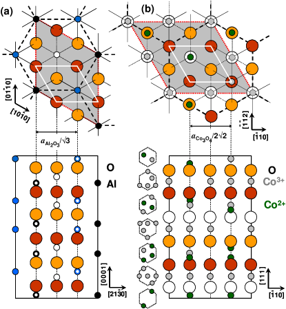
Sapphire, -Al2O3, crystalizes in the corundum structure and is the most stable aluminum oxide. -Al2O3 is rhombohedral (with two formula units in the primitive cell), but it is more conveniently described in the hexagonal representation, with lattice parameters Å, Å [21, 22, 23] for the primitive (oblique) hexagonal cell, shown in Fig. 1a following Wyckoff’s convention for the crystal axes [24]. The hexagonal primitive cell contains six formula units, with a stacking sequence of eighteen layers, in the form [Al-O3-Al]6, along the -axis. This results in three possible bulk terminations of the unit cell along the [0001] direction, consisting of planes exposing Al atoms for a truncation between two Al atomic layers, planes exposing two Al planes (Al-Al), and planes exposing O atoms, see Fig. 1a [25, 26]; the Al termination yields non-polar surfaces. Experimentally, it is observed that (0001) surfaces prepared at temperatures below 1500 K show a stable () surface, corresponding to the non-polar Al-termination; this surface is also characterized by large inward relaxation of the Al atoms [27, 28, 29, 30, 31, 32]. Annealing to higher temperatures produces a rotated () surface reconstruction, associated with the Al-rich (Al-Al) surface [33, 34, 35, 30, 36, 37, 38, 39, 40, 41]. Figure 1a shows the bulk terminated -Al2O3(0001) surface exposing an Al-Al plane. The O sublattice is close to a hexagonal close packed (hcp) lattice (A-B-A stacking, with the Al atoms occupying 2/3 of the octahedrally coordinated interstitial sites), with an O inter-plane distance of 2.166 Å along the [0001] direction.
Here, we consider the surface and interface properties of [111]-oriented epitaxial films of the prototypical Co3O4 spinel grown on -Al2O3(0001) substrates. Since the oxygen sublattices of both -Al2O3 and Co3O4 are close packed (hexagonal and face-centered cubic, respectively) with close basal lattice constants, 2.746 Å for -Al2O3 and 2.858 Å for Co3O4 (lattice mismatch of –3.9%), we may expect epitaxial growth of Co3O4 on -Al2O3(0001) to proceed as a continuation of the O-sublattice. Indeed, we show that Co3O4(111) thin films can be grown epitaxially on -Al2O3(0001) substrates by oxygen assisted molecular beam epitaxy. The as-grown Co3O4(111) surface exhibits a () surface diffraction pattern with no evidence of periodic reconstructions. The as-grown film surface shows a significant amount of disorder, which is slightly reduced upon annealing in air.
2 Sample growth and characterization techniques
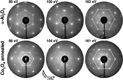
The samples for this study were grown by O-assisted molecular beam epitaxy (MBE) in a ultrahigh vacuum MBE growth system (base pressure of mbar). The substrates consist of polished -Al2O3(0001) single crystal wafers, which were annealed at 870 K in ultrahigh vacuum for 60 min, and then cleaned under an O-plasma flux at 470 K for 30 min prior to film growth. No impurities other than trace amounts of Ca were detected by Auger electron spectrocopy (AES) taken after the substrate cleaning procedure. Low energy electron diffraction (LEED) and reflection high energy electron diffraction (RHEED) of the -Al2O3(0001) substrate after cleaning display patterns characteristic of highly ordered surfaces (see Figs. 2 and 3), indicating a good crystalline order of the surface. The LEED and Laue diffraction patterns show 3-fold symmetric patterns (inner ring of the six diffraction spots in the LEED pattern show alternating intensity), suggesting that the surface is composed, predominantly, of double-layer atomic steps in the single crystalline -Al2O3(0001) surface. The cobalt oxide films were grown by oxygen-assisted molecular beam epitaxy by simultaneous exposure of the substrate to a thermally evaporated Co atomic beam and an atomic O flux. The oxygen partial pressure during growth was mbar, and the electron cyclotron resonance oxygen plasma source magnetron power was set to 175 W, yielding an atomic O flux of the order of cm-2s-1 at the sample [42, 43]. The Co evaporation rate was 2 Å/min, estimated by means of a calibrated quartz crystal microbalance. Sample growth was monitored with RHEED, and film crystallinity and electronic structure were determined immediately after growth by RHEED, LEED and XPS, entirely in ultrahigh vacuum. After film growth, the samples were characterized ex situ using x-ray diffraction (XRD), x-ray reflectometry (XRR), and atomic force microscopy (AFM). Post-growth annealing was performed at 820 K for 14 h in air; this temperature and oxygen partial pressure favor the formation of Co3O4 over CoO [44, 45, 46]. For this study, two Co3O4 samples (22 and 38 nm thick) were grown independently, which were found to have similar spectroscopic, structural and morphological characteristics (due to sample charging, no LEED patterns could be obtained for the annealed 22 nm film and for the as-grown 38 nm film).
3 Results and discussion
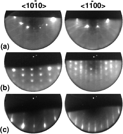
The surface crystallinity of the films was probed during growth by RHEED. The RHEED pattern evolution showed a gradual fading of the -Al2O3 sharp diffraction spots with increasing Co oxide thickness, became streaky at about 15 Å and finally broadened at about 30 Å. This indicates that film growth occurs via three-dimensional island growth. Typical RHEED patterns of the Co3O4 films after growth are shown in Fig. 2, where the in-plane crystal directions refer to those of the -Al2O3 substrate, determined independently from Laue diffraction measurements. The RHEED patterns exhibited relatively broad diffraction spots, suggesting a relatively rough surface. The diffraction patterns are characteristic of a transmission pattern of the spinel {112} planes along the azimuths of the -Al2O3 substrate (similar to the diffraction pattern of as-grown Co3O4(110) films along the [112] direction observed in [11], but rotated by 90o); and of the spinel {110} planes along the azimuths. In particular, we infer the epitaxial growth relation as Co3O4(111)[2]-Al2O3(0001)[100] and Co3O4(111)[01]-Al2O3(0001)[100]. The same epitaxial relationship is observed for MgAl2O4/-Al2O3(0001) grown by solid state reactions [47, 48]. LEED patterns for the -Al2O3(0001) substrate (Fig. 3) and for the as-grown Co3O4 film (not shown) exhibit a () diffraction pattern. Compared with the -Al2O3 LEED patterns, the diffraction spots of the as-grown Co3O4 film are much broader, and the background is also more intense, indicating that the as-grown Co3O4 films have a significant amount of surface disorder (charging of the surface also contributes to the poor patterns, especially at lower electron beam energies). Motivated by our recent results that demonstrated a significant improvement in the bulk and surface structure of Co3O4/MgAl2O4(110) thin films upon annealing [11], we have also studied the effect of post-growth annealing on the properties of Co3O4/-Al2O3(0001). RHEED patterns obtained after annealing (shown in Fig. 2 for the 38 nm film) show that annealing induces significant transformations in the film structure, as indicated by sharper and streakier RHEED diffraction patterns. However, the RHEED characteristics indicate that these surfaces are not atomically flat. LEED patterns for the annealed sample show well defined () patterns with sharp diffraction spots; although the patterns are not as sharp as for the -Al2O3 substrate and while the background is more intense, it can be inferred that the Co3O4 film surface is well ordered. Unlike the 3-fold symmetric -Al2O3 LEED patterns, the LEED diffraction patterns of the Co3O4 are 6-fold symmetric; this is usually associated with the presence of rotational twinning, i.e., the presence of both ABCA and ACBA stakings, which is known to occur in the growth of fcc (111) films on the (0001) planes of hexagonal crystals [50, 49]. Based on the geometrical configuration of our LEED system we are able to deduce the reciprocal space unit cell of the Co3O4(111) and -Al2O3(0001) surfaces (Fig. 3, left) and that of the respective O sublattices (Fig. 3, right). It is readily seen that the unit cell of the -Al2O3(0001) surface is larger (in reciprocal space) than that of Co3O4(111) and rotated by 30o, while the surface unit cell of the O sublattice are juxtaposed one on the other as expected from growth of Co3O4 as a continuation of the O sublattice. The relative spacing of the diffraction spots in the -Al2O3 and Co3O4 RHEED patterns along the direction perpendicular to the electron beam also agree with this structural model: the spacing ratio is along the azimuth and along , which correspond to and , respectively.
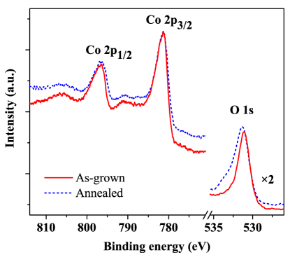
Core level XPS measurements of the Co3O4 films after growth and after annealing were carried out to assess the film stoichiometry. The XPS spectra were obtained using the Mg Kα line ( eV) of a double anode x-ray source and a double pass cylinder mirror analyzer (PHI 15-255G) set at a pass energy of 25 eV (energy resolution of about 0.8 eV). XPS spectra of the O 1s and Co 2p lines of the as-grown and annealed films are shown in Fig. 4. Corrections to the data include a five-point adjacent smoothing, x-ray satellite correction and correction of energy shifts due to charging (aligned with respect to the Co 2p peaks, using the energy assignments given in [51, 52]). One observation is that the Co 2p spectra for both samples are very similar, showing that no significant changes in stoichiometry or in the ionic state of the Co cations occur as a consequence of annealing. A second observation is that the Co 2p spectra are characteristic of a Co3O4 ionic environment [51, 52], with strongly suppressed shake-up peaks compared to those of CoO [53, 51, 52, 46, 54, 55, 56, 13]. The O 1s photoemission line is also similar before and after annealing. The additional shoulder observed at higher binding energies has been attributed to adsorbed oxygen [51, 57, 58, 59, 60, 61, 62, 13] or to surface hydroxylation [52, 13]; for the annealed sample the shoulder is much more pronounced compared to the as-grown film, consistent with surface hydroxylation through water adsorption upon exposure to air.
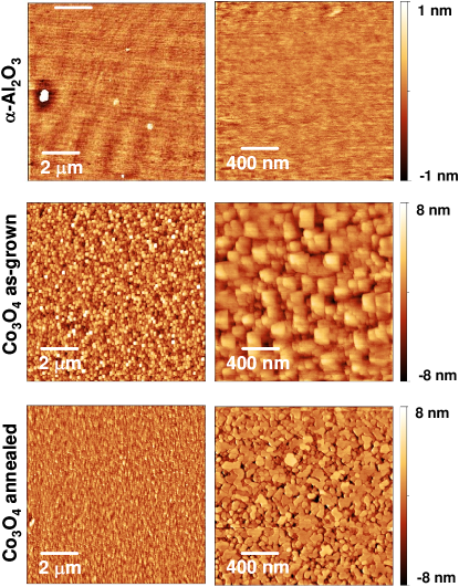
The surface morphology was also probed ex situ using atomic force microscopy (AFM) in contact mode at room temperature. The AFM data were corrected and analyzed using the Gwyddion freeware package [63]; corrections to the data included planarisation, background-correction and removal of faulty scan lines. Typical AFM surface morphology profiles for the 38 nm sample are shown in Fig. 5 for m2 and m2 scanning areas. The surface of the -Al2O3 substrate is atomically flat (average roughness of 0.2 nm), in agreement with the RHEED and LEED results. The surface profile of the as-grown Co3O4 film reveals a pronounced surface texture (rms roughness parameter of 2.4 nm), with a characteristic in-plane correlation length of about 80 nm determined from the m scans. Although regular in-plane and square in shape, these islands are not flat, in agreement with the spotty LEED and transmission-like RHEED patterns. Annealing leads to a significant change in the surface morphology, including a meandering island shape and a significant flattening of the islands, resulting in very uniform contrast in the higher magnification images. Overall, the surface is more uniform for the annealed film (rms roughness amplitude of 1.5 nm), although the island size is reduced in the process (giving an in-plane correlation length of nm for the annealed surface). The observation in AFM of smoother surfaces for the annealed film agree with the streakier RHEED patterns observed for the annealed films, and contrast with the more 3D transmission-like patterns of the as-grown films.
Structural characterization of the Co3O4 films was carried out ex situ by x-ray scattering measurements on a Shidmazu diffractometer using the Cu Kα line ( Å) with a Ni filter to remove the Cu Kβ lines. Comparison with -Al2O3 XRD spectra allows one to determine readily the diffraction peaks originating from the Co3O4 films (not shown). The XRD results show that the spectra for the as-grown and annealed films are identical in the range from , with diffraction peaks that coincide with the (hhh) planes () of Co3O4, at values corresponding to the bulk lattice parameter. This confirms the spinel crystalline phase and epitaxy of the Co3O4 film, and also that the films are fully relaxed both after growth and after annealing. In Fig. 6 we show a detail of the XRD spectra of the annealed film around the (0006) -Al2O3 peak, showing the (222) Co3O4 diffraction peak.

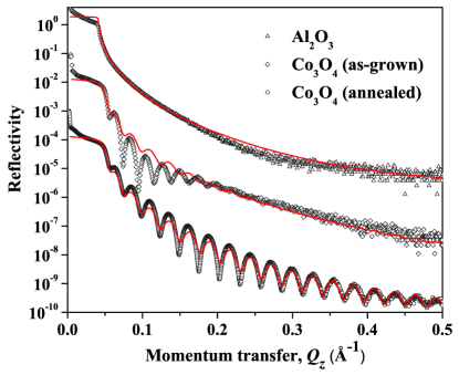
The XRR spectra of the substrate, as-grown, and annealed 22 nm Co3O4 films are shown in Fig. 7. The spectrum of the substrate (as-received) allows one to determine its surface roughness, which is estimated as 1 nm from the fit to the data (fits are shown as solid lines in Fig. 7). The reflectivity spectrum for the as-grown films show a rapid drop in the Kiessig fringes’ amplitude with momentum transfer; considering a single Co3O4 layer with bulk scattering density does not yield a good fit to the data, suggesting the presence of a non-uniform or graded interface layer. In contrast, the reflectivity spectrum of the annealed films show oscillations over the entire momentum transfer range probed, indicating a significant improvement of the interface sharpness. Fits to the data indicate that the changes occur most significantly at the -Al2O3 interface, where the roughness amplitude is found to decrease from 2.0 to 0.6 nm for the 22 nm sample, and from 4.0 to 1.5 nm for the 38 nm Co3O4 film. Hence, we interpret the strongly damped XRR spectra of the as-grown films as resulting from chemical or structural disorder at the Co3O4/-Al2O3 interface, as also suggested from the RHEED pattern evolution during growth, which shows the -Al2O3 sharp diffraction spots becoming streaky at about 15 Å and broadening at about 30 Å. In XRR, interface roughness may originate from graded interfaces, interdiffusion, and morphological roughness proper [64]. The improvement in interface sharpness upon annealing also suggests that the interface roughness in the as-grown film does not result from a reacted interface region, which should increase in thickness with annealing. Fits to the data give film thicknesses of 22.5 nm and 38.5 nm for the two samples, in good agreement with the nominal thicknesses estimated from the Co evaporation rate and the ratio between the Co3O4 and Co mass densities. The rms surface roughness of the Co3O4 films is found to increase slightly upon annealing from 1 to 2 nm for the 22 nm film, and from 2 to 2.5 nm for the 38 nm sample. The accuracy of the fits are within nm for the interface roughness and nm for the thickness.
These results are in marked contrast with those obtained for Co3O4(110)/MgAl2O4(110) films, where annealing under similar conditions results in atomically flat surfaces, associated with one particular termination of Co3O4 along the [110] direction [11]. Two factors can be expected to give rise to this difference in behaviour: the relative surface stability of the (110) and (111) crystal planes, and the role of strain in determining the surface morphology and surface roughness in particular. Surface roughening starts at the very early stages of the Co3O4(111) growth, and while this could be driven by misfit strain relaxation, we find that a similar roughening process also occurs in Co3O4/MgAl2O4(110), where the lattice mismatch is virtually zero [11]. Transmission electron microscopy results for the Co3O4/MgAl2O4(110) interface show sharp and relatively well defined interfaces [11], suggesting that the disorder observed in the XRR data could be due to modified film stoichiometry at the interface, leading to a graded interface structure; for the Co3O4/MgAl2O4(110) system the starting growth temperature was set to 770 K for the first 1 nm interface layer to optimize crystalline growth, which could lead to variations in interface composition and to a degree of interface grading. In the present study, the growth temperature was constant throughout the film growth; however, differences in the substrate and film crystal structure may favor an initial cationic arrangement closer to the corundum structure than to the spinel; for example, if the Co in the first few layers occupy an excess of octahedral sites, the film stoichiometry could be closer to Co2O3, resulting in a graded interface. This also suggests that film roughening may arise from a kinetic process common to both Co3O4/-Al2O3(0001) and Co3O4/MgAl2O4(110) systems, for example, induced by limitations in atomic surface diffusion during growth. At annealing temperatures of about 800 K, atomic diffusion is sufficient to promote surface ordering in the Co3O4 films, but while the (110) films become atomically smooth, the (111) films retain their pronounced island structure and are not atomically flat, as indicated from the AFM, XRR and RHEED results. This points to a lower stability of the (111) surface, at least under the annealing conditions.
Another intriguing aspect of this work is the fact that the polar Co3O4(111) surfaces, for both the as-grown and annealed films, are () [12], a finding similar to that found for Fe3O3(111) (depending on the growth and surface preparation conditions) [49, 65, 66] and Co3O4(110) film surfaces [11]. For Fe3O3(111) films grown on Pt(111), the () pattern was attributed to a surface structure consisting of an Fe-terminated layer, with large relaxations of the top four atomic layers, as determined from quantitative LEED intensity analysis [65]; such atomic relaxations are expected to induce strong modifications in the surface electron density of states, which could lead to charge compensation and to surface stability [65, 6]. The results for the Co3O4 surfaces have been explained in terms of a charge compensation mechanism consisting of a surface spinel inversion process, whereby tetrahedral Co2+ cations revert to a trivalent state [12, 11], leading to stable () surfaces. We envisage that a similar mechanism may be in play for the (111) surface.
4 Conclusions
In summary, we have demonstrated epitaxial growth of Co3O4(111) thin films on -Al2O3(0001) by oxygen assisted molecular beam epitaxy. The films grow with the Co3O4 stoichiometry, which remains unchanged upon post-growth annealing. However, the interface and surface structure of the Co3O4(111) film changes considerably upon annealing. Annealing leads to a significant improvement of the Co3O4/-Al2O3 interface structure, while the Co3O4/air interface is also strongly modified. Unlike Co3O4/MgAl2O4(110), annealing does not lead to atomically smooth surfaces in Co3O4/-Al2O3(0001). Stable () surfaces are observed in both as-grown and annealed films, which is explained by a surface spinel inversion process that leads to surface charge compensation.
Acknowledgements
The authors acknowledge financial support by the NSF through MRSEC DMR 0520495 (CRISP), MRSEC DMR 0705799, the ONR (C.H.A.), and the U.S. Department of Energy Basic Energy Sciences Grant Numbers DEFG02-98ER14882 and DE-FG02-06ER15834 (E.I.A.).
References
- [1] J. P. Picard, G. Baud, J. P. Besse, R. Chevalier, Journal of the Less-Common Metals 75 (1980) 99.
- [2] J. Chenavas, J. C. Joubert, M. Marezio, Solid State Commun. 9 (1971) 1057.
- [3] G. V. Samsonov (Ed.), The oxide handbook, 2nd Edition, IFI/Plenum, New York, 1982.
- [4] M. Catti, G. Sandrone, Faraday Discuss. 106 (1997) 189.
- [5] P. W. Tasker, J. Phys. C: Solid State Phys. 12 (1979) 4977.
- [6] C. Noguera, J. Phys.: Condens. Matter 12 (2000) R367.
- [7] J. Goniakowski, F. Finocchi, C. Noguera, Rep. Prog. Phys. 71 (2008) 016501.
- [8] W. A. Harrison, E. A. Kraut, J. R. Waldrop, R. W. Grant, Phys. Rev. B 18 (1978) 4402.
- [9] M. Gajdardziska-Josifovska, R. Plass, M. A. Schofield, D. R. Giese, R. Sharma, J. Electron Microsc. 51 (2002) S13.
- [10] V. K. Lazarov, R. Plass, H.-C. Poon, D. K. Saldin, M. Weinert, S. A. Chambers, M. Gajdardziska-Josifovska, Phys. Rev. B 71 (2005) 115434.
- [11] C. A. F. Vaz, H. Wang, C. H. Ahn, V. E. Henrich, M. Z. Baykara, T. Schwendemann, N. Pilet, B. J. Albers, U. Schwarz, L. H. Zhang, Y. Zhu, J. Wang, E. I. Altman, Surf. Sci. 603 (2009) 291.
- [12] W. Meyer, K. Biedermann, M. Gubo, L. Hammer, K. Heinz, J. Phys.: Condens. Matter 20 (2008) 265011.
- [13] S. C. Petitto, E. M. Marsh, G. A. Carson, M. A. Langell, J. Molecular Catalysis A: Chemical 281 (2008) 49.
- [14] X. Tang, J. Li, J. Hao, Materials Research Bulletin 43 (2008) 2912.
- [15] C. M. Fang, S. C. Parker, G. de With, J. Am. Ceram. Soc. 83 (2000) 2082.
- [16] M. J. Davies, S. P. Parker, G. W. Watson, J. Mater. Chem. 4 (1994) 813.
- [17] R. L. Stewart, R. C. Bradt, J. Mater. Sci. 15 (1980) 67.
- [18] R. C. Bradt, Cleavage of ceramic and mineral single crystals, in: K. S. Chan (Ed.), George R. Irvin Symposium on Cleavage Fracture, Warrendale, PA, 1997, p. 355.
- [19] C. M. Fang, G. de With, S. C. Parker, J. Am. Ceram. Soc. 84 (2001) 1553.
- [20] N. J. van der Laag, A. J. M. van Dijk, N. Lousberg, G. de With, L. J. M. G. Dortmans, J. Am. Ceram. Soc. 88 (2005) 660.
- [21] R. E. Newnham, Y. M. D. Haan, Zeitschrift für Kristallographie 117 (1962) 235.
- [22] C. S. G. Cousins, J. Phys. C: Solid State Phys. 14 (1981) 1585.
- [23] A. Kirfel, K. Eichhorn, Acta Cryst. A 46 (1990) 271.
- [24] R. W. G. Wyckoff, Crystal structures, 2nd Edition, Vol. 2, Interscience Publishers, New York, 1964.
- [25] J. Guo, D. E. Ellis, D. J. Lam, Phys. Rev. B 45 (1992) 13647.
- [26] T. J. Godin, P. LaFemina, Phys. Rev. B 49 (1994) 7691.
- [27] I. Manassidis, A. D. Vita, M. Gillan, Surf. Sci. Lett. 285 (1993) L517.
- [28] J. Ahn, J. Rabalais, Surf. Sci. 388 (1997) 121.
- [29] P. Guénard, G. Renaud, A. Barbier, M. Gautier-Soyer, Surf. Rev. Lett. 5 (1997) 321.
- [30] G. Renaud, Surface Science Reports 32 (1998) 1.
- [31] E. A. A. Jarvis, E. A. Carter, J. Phys. Chem. B 105 (2001) 4045.
- [32] E. Wallin, J. M. Andersson, E. P. Münger, V. Chirita, U. Helmersson, Phys. Rev. B 74 (2006) 125409.
- [33] C. C. Chang, J. Appl. Phys. 39 (1990) 5570.
- [34] T. M. French, G. A. Somorjai, J. Appl. Phys. 74 (1970) 2489.
- [35] V. E. Henrich, P. A. Cox, The surface science of metal oxides, Cambridge University Press, Cambridge, 1994.
- [36] T. Suzuki, S. Hishita, K. Oyoshi, R. Souda, Surf. Sci. 437 (1999) 289.
- [37] C. F. Walters, K. F. McCarty, E. A. Soares, M. A. Van Hove, Surf. Sci. 464 (2000) L732.
- [38] C. Barth, M. Reichling, Nature 414 (2001) 54.
- [39] E. A. Soares, M. A. Van Hove, C. F. Walters, K. F. McCarty, Phys. Rev. B 65 (2002) 195405.
- [40] A. Marmier, S. C. Parker, Phys. Rev. B 69 (2004) 115409.
- [41] J. A. Kelber, Surf. Sci. Rep. 62 (2007) 271.
- [42] W. Gao, R. Klie, E. Altman, Thin Solid Films 485 (2005) 115.
- [43] R. Anton, T. Wiegner, W. Naumann, M. Liebmann, C. Klein, C. Bradley, Rev. Sci. Instrum. 71 (2000) 1177.
- [44] H. P. Tripp, B. W. King, J. American Ceramic Soc. 38 (1955) 432.
- [45] K. Koumoto, H. Yanagida, Jpn. J. Appl. Phys. 20 (1981) 445.
- [46] M. Oku, Y. Sato, Appl. Surf. Sci. 55 (1992) 37.
- [47] R. C. Rossi, R. M. Fulrath, J. Am. Ceram. Soc. 46 (1963) 145.
- [48] C.-M. Liu, J.-C. Chen, C.-J. Chen, J. Crystal Growth 285 (2005) 275.
- [49] Y. Gao, Y. J. Kim, S. A. Chambers, G. Bai, J. Vac. Sci. Technol. A 15 (1997) 332.
- [50] M. J. Stowell, Defects in epitaxial deposits, in: J. W. Matthews (Ed.), Epitaxial growth, Part B, Academic Press, Inc., 1975, p. 437.
- [51] T. J. Chuang, C. R. Brundle, D. W. Rice, Surf. Sci. 59 (1976) 413.
- [52] J. Haber, L. Ungier, J. Electron Spectrosc. Relat. Phenom. 12 (1977) 305.
- [53] J. P. Bonnelle, J. Grimblot, A. D’Huysser, J. Electron Spectrosc. Relat. Phenom. 7 (1975) 151.
- [54] M. A. Langell, M. D. Anderson, G. A. Carson, L. Peng, S. Smith, Phys. Rev. B 59 (1999) 4791.
- [55] H. A. Hagelin-Weaver, G. B. Hoflund, D. M. Minahan, G. N. Salaita, Appl. Surf. Sci. 235 (2004) 420.
- [56] H.-Q. Wang, E. I. Altman, V. E. Henrich, Phys. Rev. B 77 (2008) 085313.
- [57] Y. Jugnet, T. M. Duc, J. Phys. Chem. Solids 40 (1979) 29.
- [58] Y. M. Kolotyrkin, I. D. Belova, Y. E. Roginskaya, V. B. Kozhevnikov, D. S. Zakhar’in, Y. N. Venevtsev, Materials Chemistry and Physics 11 (1984) 29.
- [59] B. Klingenberg, F. Grellner, D. Borgmann, G. Wedler, Surf. Sci. 296 (1993) 374.
- [60] B. Klingenberg, F. Grellner, D. Borgmann, G. Wedler, J. Electron Spectrosc. Relat. Phenom. 71 (1995) 107.
- [61] V. M. Jiménez, A. Fernández, J. P. Espinós, A. R. González-Elipe, J. Electron Spectrosc. Relat. Phenom. 71 (1995) 61.
- [62] G. A. Carson, M. H. Nassir, M. A. Langell, J. Vac. Sci. Technol. A 14 (1996) 1637.
- [63] http://gwyddion.net
- [64] M. Wormington, I. Pape, T. P. A. Hase, B. K. Tanner, D. K. Bowen, Phil. Mag. Lett. 74 (1996) 211.
- [65] M. Ritter, W. Weiss, Surf. Sci. 432 (1999) 81.
- [66] I. V. Shvets, N. Berdunov, G. Mariotto, S. Murphy, Europhys. Lett. 63 (2003) 867.