Frequency dependence of the radiative decay rate of excitons in self-assembled quantum dots: experiment and theory
Abstract
We analyze time-resolved spontaneous emission from excitons confined in self-assembled quantum dots placed at various distances to a semiconductor-air interface. The modification of the local density of optical states due to the proximity of the interface enables unambiguous determination of the radiative and non-radiative decay rates of the excitons. From measurements at various emission energies we obtain the frequency dependence of the radiative decay rate, which is only revealed due to the separation of the radiative and non-radiative parts. It contains detailed information about the dependence of the exciton wavefunction on quantum dot size. The experimental results are compared to the quantum optics theory of a solid state emitter in an inhomogeneous environment. Using this model, we extract the frequency dependence of the overlap between the electron and hole wavefunctions. We furthermore discuss three models of quantum dot strain and compare the measured wavefunction overlap to these models. The observed frequency dependence of the wavefunction overlap can be understood qualitatively in terms of the different compressibility of electrons and holes originating from their different effective masses.
pacs:
78.67.Hc, 42.50.Ct, 78.47.-pI Introduction
Semiconductor quantum dots (QDs) are nanoscale solid state structures that provide three-dimensional quantum confinement of otherwise mobile charge carriers. Self-assembled QDs of embedded in provide confinement for both electrons and holes in a direct band gap semiconductor. Hence, they are optically active with the benefits of a high quantum efficiency and compatibility with existing semiconductor technology. These properties make the QDs highly promising light sources for novel optical devices including optical quantum information devices Imamoglu et al. (1999). This has led to an increasing interest in the quantum-optical properties of QDs, and major achievements include the demonstration of the Purcell effect for QDs in solid-state cavities Gérard et al. (1998) and strong coupling between a single QD and the optical mode of a cavity Reithmaier et al. (2004); Yoshie et al. (2004). Very recently also electrical tuning of such quantum photonics devices was demonstrated Kistner et al. (2008); Laucht et al. (2008), which is a significant milestone towards practical all-solid state cavity quantum electrodynamics devices.
Despite the recent progress, a thorough understanding of the dynamics of light-matter coupling for QDs in nanostructured photonic media is still lacking. Such an understanding is required for quantitative comparisons between experiment and theory. The problem is two-fold, i.e. a detailed understanding of both the optical part and the electronic part is required. The optical part is described by the local density of optical states (LDOS) expressing the distribution of modes that the QD can radiate to, while the electronic part is determined by the exciton wavefunction for the QD. Here we will investigate an optical system where the LDOS can be calculated exactly, and use that to extract detailed information about the QD. Our experimental results are compared to a theoretical QD model, and the effect of QD size, material composition, and strain is investigated. Such quantitative comparisons of experimental data to simple theoretical QD models are much needed in order to assess the full potential of QDs in nanostructured media for, e.g., single-photon sources Michler et al. (2000), low-threshold lasers Reitzenstein et al. (2008), or spontaneous emission control Lodahl et al. (2004); Julsgaard et al. (2008).
When interpreting spontaneous emission decay curves from QDs, it is often implicitly assumed that the QDs primarily decay through radiative recombination, while non-radiative processes are negligible. Unfortunately, this assumption is not generally valid, and omnipresent non-radiative processes must be considered. Only few experiments have addressed this issue. Robert et al. established an upper bound on the contribution from nonradiative processes of 25% by measuring the ratio of the bi-exciton to exciton emission intensity at saturation Robert et al. (2002). Quantitative measurements of the radiative and non-radiative decay rates of QDs were only carried out recently using a modified LDOS both for colloidal QDs Brokmann et al. (2004); Leistikow et al. (2009) and for self-assembled QDs Johansen et al. (2008a). Precise measurements of the radiative decay rates are essential since nanophotonic devices rely on the ability to manipulate the radiative processes, while non-radiative recombination leads to loss in the system.
As first pointed out by Purcell Purcell (1946) the radiative decay rate of an emitter is modified inside a structured dielectric medium, which is due to the modification of the LDOS. In early experiments by Drexhage Drexhage (1970), this effect was experimentally demonstrated by positioning emitters in the proximity of a reflecting surface. We have recently employed the modified LDOS near a semiconductor-air interface as a spectroscopic tool to extract radiative and non-radiative decay rates and from that infer the overlap between the electron and hole wavefunctions Johansen et al. (2008a). This technique relies on the fact that the radiative decay rate is proportional to the LDOS, while the non-radiative decay rate is unaffected. In the present paper we expand on our previous work in particular by comparing the measured radiative decay rate to theory, which requires a detailed model of the QD electron and hole wavefunctions. We have measured the radiative decay rate at different emission energies, which reveals the dependence of the QD optical properties on its size. We review the Wigner-Weisskopf theory of spontaneous emission from QDs, predicting an exponential decay of the exciton population and the LDOS is derived for the applied interface geometry using a Green’s function technique. We furthermore show that the radiative decay rate of a QD in a homogeneous medium is proportional to the square of the overlap between electron and hole wavefunctions and calculate the frequency dependence of this overlap using a simple two-band model of the QD. The QD model is discussed in details and compared to our experimental data employing realistic parameters as input to the theory. The pronounced size dependence of the electron-hole wavefunction overlap is found to originate from the differences in effective mass and binding energy of the electron and hole. Furthermore, we investigate three different strain models for the QD and compare their predictions to experiment thereby providing valuable insight on the complex strain mechanisms of self-assembled QDs.
This paper is organized as follows: In section II we present the experimental method and in section III the experimental results. In section IV we discuss the Wigner-Weisskopf model for spontaneous emission and derive the relation between the radiative decay rate, the LDOS, and the wavefunction overlap. In section V we combine the analytical expressions for the radiative rate with the numerical results for the wavefunction overlap and compare theory with experiment. Finally, we present conclusions in section VI.
II Experimental technique for determining the radiative decay rate of quantum dots
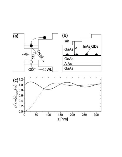
Spontaneous emission of a photon from a QD occurs when an electron-hole pair (an exciton) recombines, as illustrated schematically in Fig. 1(a). As will be shown rigorously in section IV, the QD radiative decay rate in a structured environment is proportional to the projected local density of optical states (LDOS) , where the projection is along the direction of the transition momentum matrix element, which corresponds to the orientation of the transition dipole moment. The LDOS is modified in an inhomogeneous dielectric medium due to optical reflections at interfaces. In emission experiments, the total decay rate is measured, which can be expressed as Novotny and Hecht (2007)
| (1) |
where is the density of optical states for a homogeneous medium, and is the rate for non-radiative recombination. is the emission frequency and thus the emission energy, and the position of the QD. Non-radiative recombination is due to intrinsic QD processes and thus independent of the LDOS. is the radiative rate that the QD would exhibit in a homogenous medium without any boundaries. In our case, the refractive index of the medium is corresponding to that of . Investigating in detail provides valuable insight into the properties of the exciton wavefunction confined in the QD potential.
The exact nature of non-radiative recombination in QDs is not yet fully understood. It is often implicitly assumed that non-radiative recombination is negligible, but as we will see in the following even for very weak excitation intensities this is not a valid assumption. Possible non-radiative processes include surface recombination at the interfaces between the QD and the surrounding semiconductor material, Auger processes, and trapping of electron and/or holes at defects Chuang (1995), and any first principles calculation of these effects is a tremendous task. Reliable ways of extracting the radiative and non-radiative parts of the decay rate are therefore essential.
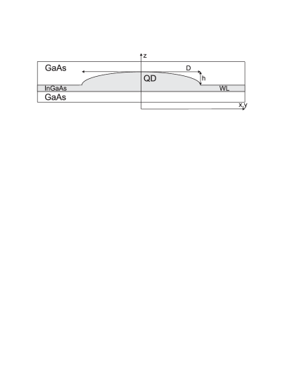
The radiative and non-radiative decay rates can be separated by time-resolved spontaneous emission measurements if the QDs are placed in an environment with a known LDOS, cf. Eq. (1). A planar interface between two regions with different refractive indices is the most simple example of such an inhomogeneous dielectric medium Chance et al. (1978). For this particular geometry, the LDOS can be calculated exactly and without any free parameters. Here we employ the interface between GaAs () and air () as illustrated in Fig. 1(b). We calculate the LDOS by a Green’s function technique and the results for dipole orientations parallel or perpendicular to the interface are shown in Fig. 1(c). We stress that no assumptions need to be made about, e.g., the QD density and the excitation beam profile in order to employ this experimental technique, as opposed to alternative ways of determining the radiative decay rate such as by absorption spectroscopy Birkedal et al. (2000); Warburton et al. (1997); Silverman et al. (2003).
III Measurements of spontaneous emission decay rates near a semiconductor-air interface
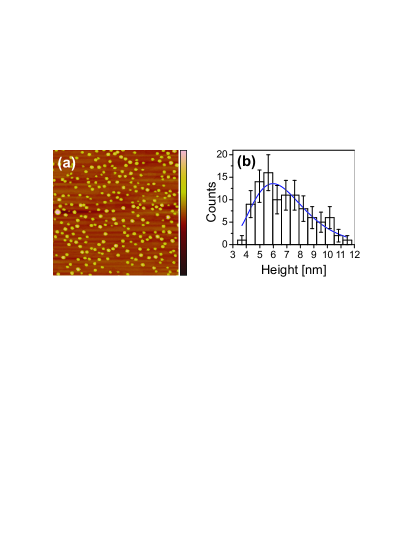


The starting point of our investigations is a wafer grown by molecular beam epitaxy (MBE). The QDs were grown using the Stranski-Krastranow method on a (001) substrate. The growth sequence was AlAs, , 2.0 monolayers (MLs) , cap, and finally 2.0 ML . The AlAs layer was included for an optional epitaxial lift-off process, which was not employed here. Both layers formed self-assembled QDs, but only the embedded layer was optically active because non-radiative surface recombination dominates for QDs at the surface. However, since the QDs at the surface were fabricated under identical growth conditions as the embedded ones, the density of the active QDs can be determined by atomic force microscopy (AFM) of the sample surface. Such an atomic force micrograph is shown in Fig. 2(a). The image contains detailed information about the geometry and height of the QDs at the surface, but the topography of the surface is convolved with the AFM tip shape function, and thus the width and exact geometry of the QDs cannot be extracted directly. The maximum height, however, is not subject to this effect and we used the AFM data in Fig. 2(a) to obtain a histogram of the heights recorded for 100 randomly selected QDs. The result is shown in Fig. 2(b). We fit the height histogram by a log-normal distribution given by with , , and , where is a dimensionless length scale normalized to 1 . We find an average aspect ratio defined as the height to lateral base diameter ratio of , but due to the convolution effect this is an upper bound. Since the transition energy of a QD depends sensitively on its height, the height distribution function is central when testing theoretical models of the emission spectrum against experiments, as discussed in section V.
From the AFM data we found a QD density of 250 which corresponds to an average interdot distance of 60 . This number should be compared to typical length scales for various relevant QD interactions. Carrier tunneling is negligible for distances beyond 15 Wang et al. (2004) and the dipole-dipole interaction is only significant for distances close to the Förster radius, which is typically 2-9 Novotny and Hecht (2007). Therefore the measurements performed here provide ensemble averaged values of single QD properties with the advantage of an excellent signal-to-noise ratio in the measurements.
The wafer was processed by standard UV lithography and wet chemical etching in five subsequent steps with nominal etch depths of , , , , and by which we obtained 32 fields with specific distances from the QDs to the semiconductor surface. The 32 fields were nominally equidistantly spaced with spacing. The wet etching was done using an etchant comprised of (85%), (30%), and in the ratio , which has an etch rate on at room temperature of 1 . We found that this etchant results in surfaces of good optical quality with low surface roughness. A schematic illustration of the resulting sample is shown in Fig. 1(b). Finally we measured the actual distance from the QDs to the semiconductor surface by using a combination of secondary ion mass spectroscopy and surface profiling from which we found typical depth uncertainties of .
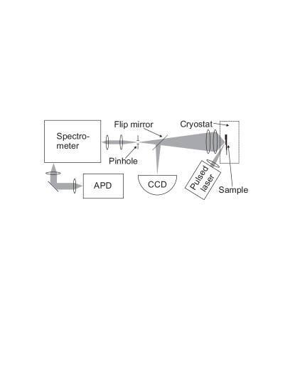
The experimental setup is illustrated in Fig. 3. The sample was kept at and irradiated by a mode-locked Ti:sapphire laser emitting 300 pulses at 1.45 , which corresponds to excitation of the wetting layer states of the QD ensemble. The repetition rate was 80 and we used an excitation intensity of 7 , which corresponds to less than 0.1 excitons per QD generated in the wetting layer per pulse, i.e. only the QD ground state is populated. Excitation of the WL states is advantageous since the same density of excitons is generated independent of sample thickness, which would not be the case for excitation in the barrier since the samples have different thicknesses. The pump configuration is illustrated in Fig. 1(a). The spontaneous emission from the QD ensemble was collected and then dispersed by a monochromator with a spectral resolution of 2.6 from which it was directed onto a fast silicon avalanche photodiode (APD).
Representative examples of two decay curves obtained for two different distances to the interface are shown in the inset of Fig. 4(a). We model our data with a bi-exponential decay and typically find a goodness-of-fit parameter Lakowicz (2006) of 1.2, which is close to the ideal value of unity, thus confirming the validity of the model. The important parameter extracted from the fit is the fast decay rate, which is due to recombination of bright excitons in the QD, i.e., it equals the total decay rate discussed in the previous section.
We measured the decay curves for 32 nominally equidistantly spaced distances to the interface. We found that for the two distances closest to the interface there was no detectable spontaneous emission due to the very close proximity of the interface and/or damage by the etching process. In Fig. 4(a) we show the extracted fast decay rates (upper trace) versus the measured distance from the QDs to the interface for the remaining samples. As shown in Fig. 4(b) we obtain values of near unity for the bi-exponential fits for all distances. The solid blue curve is a fit to the fast decay rates using the calculated LDOS for a dipole oriented parallel to the interface. When omitting the seven data points closest to the interface, as discussed in detail below, we find an excellent agreement with theory. Since the slow rate (lower trace) does not depend on the distance to the interface and therefore does not depend on the LDOS it must be dominated by non-radiative decay. It is attributed as due to the recombination of dark excitons and the dynamics will be the subject of a future publication Johansen et al. (2008b). In the remainder of this paper we will consider only the fast decay rate.
When plotting the fast decay rates as a function of the LDOS normalized to the density of states of a homogeneous medium, a linear dependence is expected, see Fig. 5(a). However, close to the interface the measured decay rate is found to be systematically larger than expected by theory. This deviation could be due to enhanced recombination rates induced by, e.g., scattering or impurities at the semiconductor surface. In order to exclude these effects in our analysis of intrinsic QD properties, we systematically excluded the data points closest to the interface in the fit. We found that the linear regression correlation parameter Barford (1990) obtained from the fit in Fig. 5(a) saturated close to the ideal value of unity when excluding the seven innermost data points, see Fig. 5(b). These points were consequently abandoned in the analysis. For distances we find an excellent agreement between theory and experiment, which allows reliable extraction of the radiative and non-radiative rates of the QDs.
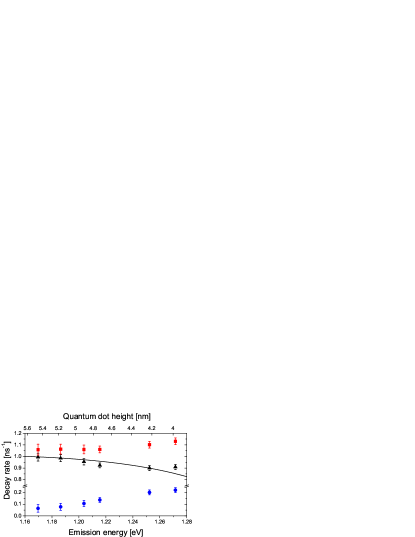
The linear fit in Fig. 5(a) is based on Eq. (1) and contains two free parameters, namely the homogeneous radiative decay rate and the non-radiative decay rate . We obtain and at an emission energy of . For reference, the theoretical curve for a dipole oriented perpendicular to the interface (i.e. parallel to the growth direction) is shown in Fig. 1(c). Clearly, this model cannot fit the experimental data, which confirms that the QDs are oriented in the plane perpendicular to the growth direction, which was previously established by absorption measurements Cortez et al. (2001). We measured the decay curves at six energies across the inhomogeneously broadened emission spectrum. When extracting the fast rate from the fits, we obtain the curves shown in Fig. 6. The different emission frequencies shift the curves along the abscissa and more importantly the amplitude and ordinate offsets are changing, which corresponds to changes in and . This shows directly the frequency dependence of and , which will be discussed below.
The total decay rate in a homogeneous medium was extracted from Fig. 6 by the method outlined above and the result is shown in Fig. 7(a). The total decay rate increases with increasing emission energy, which could suggest that the radiative rate increases with energy, as has been reported for colloidal QDs van Driel et al. (2005). However, the opposite turns out to be true for self-assembled QDs. In this case, is found to decrease with increasing energy, and the overall increase in the total rate is due to the pronounced increase in with emission energy. It should be stressed that such variations in the radiative rate can be assessed only because a modified LDOS is employed allowing to separate radiative and non-radiative contributions. The striking energy dependence of the radiative rate can be explained as being due to the dependence of the electron and hole wavefunctions on the size of the QD, which will be discussed and analyzed in detail in section V.
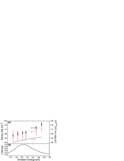
Here we want to stress some potential pitfalls in the interpretation of the frequency dependence of spontaneous emission decay rates from QDs. As already pointed out, it is decisive to include the effects of non-radiative recombination and implement a technique that allows to separate it from radiative recombination. Thus, an a priori assumption of negligible non-radiative recombination would erroneously lead to the conclusion that the radiative rate increases with energy. Furthermore, when extracting quantitative data for the QD decay rates, one has to be aware of the possible influence of the presence of interfaces. In a homogeneous medium the LDOS is proportional to the emission energy squared, but this is not the case in proximity of interfaces. In Fig. 8(a) we compare the measured total decay rate versus emission energy for an unprocessed wafer and compare to the total rate that QDs in a homogeneous medium would exhibit. The latter has been obtained using the LDOS technique explained above and provides ”undisturbed” QD properties. For the unprocessed wafer, the distance to the interface is 302 and for this distance the LDOS increases with increasing energy, cf. the solid blue line in Fig. 8(a). This frequency dependence of the LDOS modifies the measured emission rates, which should be taken into account, and is an example of the importance of considering nearby interfaces in quantitative assessment of QD properties. Experimentally this issue could be solved by growing a very thick capping layer on top of the QDs.
IV Theoretical description of spontaneous emission from quantum dots due to interaction with the quantized electromagnetic field
In this section, we give a theoretical description of the radiative decay of excitons in QDs. For sufficiently small QDs, the energy difference between bound states in the QDs is much larger than the Coulomb energy and the effect of the Coulomb interaction on the internal exciton dynamics becomes negligible Hanamura (1988). This means that the electron and hole comprising the exciton may be considered independent, which is the strong confinement model. Furthermore, we employ here a two-band description of the QD including the effects of a wetting layer and strain, which is sufficient to capture the essential properties of QDs Melnik and Willatzen (2004); Markussen et al. (2006). Our objective here is to explore the validity of this model by a thorough comparison to our measurements of the radiative decay rate and the emission spectrum, which is carried out in section V. Thorough explorations of even simple QD models are much needed since complete microscopically correct QD models are outside reach both due to the lack of experimental knowledge about exact atomic composition and computational complexity.
Spontaneous emission occurs due to the interaction of the exciton with the continuum of vacuum modes. A rigorous description of spontaneous emission requires a fully quantum description where both the radiation field and the exciton states in the QD are quantized. We employ here the Wigner-Weisskopf model of spontaneous emission, which is valid when the LDOS varies slowly with frequency over the linewidth of the QD. This is an excellent approximation for the dielectric structures investigated here, but may break down for QDs in photonic crystal leading to intricate non-Markovian dynamics Kristensen et al. (2008). The radiative coupling strength is determined by the electron momentum matrix element and depends furthermore sensitively on the overlap between the electron and hole envelope wavefunctions that in turn gives rise to the frequency dependence of the radiative decay rate. We derive here this frequency dependence, which will be compared in detail to the experimental data in section V.
IV.1 Wigner-Weisskopf theory of spontaneous emission from quantum dots
According to effective mass theory, the solution to the Schrödinger equation for an electron in a solid is given by , where is the envelope function, is the Bloch function evaluated at the band edge , and denotes the conduction () or valence () band. The envelope function is the solution to the effective mass Schrödinger-like equation governed by the Hamiltonian Li et al. (1996)
| (2) |
where is the kinetic energy operator, and is the band confinement potential. Here we consider lens-shaped QD geometries as shown in Fig. (9). For the conduction band the effective mass is isotropic, so that , where is the elementary electron mass and is the effective mass. For the valence band the anisotropy of the effective mass must be taken into account, which is discussed in Appendices A and B.
For the valence band and , which leads to negative eigenenergies. In the electron-hole representation Haug and Koch (1994) we define the hole in the valence band as a particle with positive effective mass subject to a positive confinement potential yielding positive eigenenergies. Clearly, the envelope function remains the same in the new representation, i.e. . For III-V semiconductors the valence band is comprised of degenerate bands with different effective masses. However for QDs strain lifts this degeneracy and we may consider the valence band as a single band (the heavy hole band). We discuss details of the band structure in the presence of strain in Appendix A.
We describe the light-matter interaction by the Hamiltonian , where is the elementary charge, is the momentum operator and is the vector potential of the quantized electromagnetic field. The latter is given by Vats et al. (2002); Loudon (2000)
| (3) |
Here is the combined wavevector and polarization index , is the optical angular frequency, is a normalization constant with denoting the vacuum permittivity, is a unit vector in the direction of the polarization , is the spatial field distribution function, and and are the field annihilation and creation operators, respectively. In a homogeneous medium the field distribution functions are given by plane waves , where is the relative static permittivity of the material. We will be working in the Coulomb gauge in which the scalar potential of the electromagnetic field is zero and the divergence of the vector potential vanishes.
We consider the initial state with corresponding to a QD with one electron promoted to the conduction band and no photons in the radiation field. The final state relevant for spontaneous emission is with , where a photon is radiated to the mode while the excited electron has decayed to the valence band. We have deliberately not written the spatial dependence of and for visual clarity. We can expand the interaction Hamiltonian by insertion of complete sets to obtain an expression containing the raising and lowering operators of the electronic system, which we define as and , respectively. It is convenient to change to the interaction picture, in which the time-evolution of the raising and lowering operators are given by and , where we have introduced the energy of the exciton transition . Furthermore, assuming that the spatial distribution functions are slowly varying on the scale of the wavefunctions they can be evaluated at the center position of the QD, which is the dipole approximation. The interaction Hamiltonian in the interaction picture now reads
| (4) | ||||
where and we have omitted the two terms proportional to since they are rapidly oscillating as a function of time, which is the rotating wave approximation.
The general state vector of the system can be expanded as
| (5) |
and inserting into the Schrödinger equation in the interaction picture leads to the following equation of motion Vats et al. (2002)
| (6) |
where we have included an integration over a Dirac delta function in frequency, and assumed that the momentum matrix element is constant within the linewidth of the QD. is the projected LDOS defined as
| (7) |
where is the unit vector specifying the direction of . This direction is determined by the Bloch matrix element as discussed below. Since in Eq. (6) is slowly varying over the linewidth of the emitter so that it can be evaluated at the emission frequency and taken outside the integral. In this case the QD population decays exponentially with the radiative decay rate given by
| (8) |
This is the Wigner-Weisskopf result for spontaneous emission from solid-state emitters. It states that the radiative decay rate is proportional to the projected LDOS and the momentum matrix element. In the following subsection, we discuss the evaluation of these two terms. In the experiment, the number of photons emitted per time is measured, which is given by
| (9) |
where additionally the rate for non-radiative recombination has been added, and is an overall scaling parameter determined by the detection efficiency and the total number of photons recorded during the measurement period.
IV.2 Evaluation of the projected LDOS and the transition matrix element
The projected LDOS can be calculated using a Green’s function technique. In terms of the Green’s tensor , the projected LDOS is given by Novotny and Hecht (2007); Dung et al. (2000)
| (10) |
where is the speed of light in vacuum. The LDOS is a classical electromagnetic quantity obtained by solving Maxwell’s equations. However, it enters the quantum optical theory of light-matter interaction where it describes the local density of vacuum modes that spontaneous emission can occur to. For the particular case of a semiconductor-air interface as considered here, the Green’s tensor is obtained by solving the following closed expression Paulus et al. (2000); Novotny and Hecht (2007)
| (11) |
where
| (15) |
and
| (19) |
Here , where is the -vector in cylindrical coordinates, is the distance from the QD to the interface, and () is the Fresnel reflection coefficient for s-polarized (p-polarized) light Novotny and Hecht (2007). The result of the calculation for a -air interface is shown in Fig. 1(c)
We now consider the transition matrix element. Using the fact that the momentum operator is a differential operator , that the Bloch functions are orthogonal, which we will describe below, and that the envelope functions are slowly varying on the scale of a lattice parameter Coldren and Corzine (1995), we obtain
| (20) | ||||
This important result states that the transition matrix element is given by the product of the electron and hole wavefunction overlap and the squared Bloch matrix element . The magnitude of the Bloch matrix element is a material parameter that is expressed in terms of the Kane energy Coldren and Corzine (1995). is the indium mole fraction in the alloy. The
In the Kane model Chuang (1995); Davies (1998) the valence band Bloch functions are written as linear combinations of the basis functions , , and that carry the symmetry properties of p-orbitals. The specific linear combination depends on the -vector of the envelope function. QDs grown by the Stranski-Krastanov technique are typically flat structures placed on top of a wetting layer, and quantization along the growth direction is therefore dominating Andreev and O’Reilly (2005). As a consequence we can set , which is exact in the limit of a quantum well, leading to . In this case the heavy hole Bloch function can be written as . The conduction band Bloch function has s-symmetry, so the Bloch functions for the valence and conduction bands are orthogonal as was used above. Furthermore, this means that the matrix element is non-zero only for and from which we conclude that the dipole axis of the QD is perpendicular to the growth direction in agreement with our experiment.
IV.3 Frequency dependence of the radiative decay rate of quantum dots
We are now in a position to put together the results of the previous sections and calculate the frequency dependence of the spontaneous emission decay rates in a homogenous medium. By insertion of Eq. (7) in Eq. (8) and using the plane wave expression for the field distribution functions we readily obtain
| (21) | ||||
The sum over all optical modes can be converted to an integration over all k-vectors where the dispersion relation for a homogeneous medium is used. The sum over polarizations yields a factor of . Using also Eq. (20) we obtain the important relation
| (22) |
Here we have indicated explicitly that the envelope wavefunctions depend on the emission energy since varying the QD size, and thereby the emission energy, leads to modifications of the wavefunctions. This effect will be discussed in detail in section V. Eq. (22) is the key result used to interpret the experimental measurements of the radiative decay rate presented in this paper. It furthermore allows extracting an experimental value for the overlap between the electron and hole wavefunctions.
V Comparison between experiment and theory for the electron-hole wavefunction overlap
In this section we calculate the electron-hole wavefunction overlap and the QD emission spectrum and compare to our experimental results. We investigate to what extent the QD heights obtained from AFM measurements of uncapped QDs, cf. Fig. 2, can be used as input to the models. Furthermore, we systematically test the model with experiment by varying parameters such as the indium mole fraction, the QD aspect ratio, the wetting layer thickness, and the applied strain model within physically realistic boundaries. The model nicely reproduces the decrease of the electron-hole wavefunction overlap with energy that we observed experimentally. However, our investigations lead to the conclusion that further knowledge of QD composition and more involved QD models would be required in order to reach full quantitative agreement between experiment and theory.
We describe the QD in the -plane as one quarter of an ellipse with a fixed aspect ratio. Here denotes the radial direction in cylindrical coordinates. The QD geometry is solved numerically in a large simulation area which spans in the -direction and in the -direction ensuring that the proximity of the boundaries have no effect on the results. Further details on the numerical procedure is provided in Appendix B. We use the commercial finite element software package COMSOL with an adaptive mesh to solve the effective mass equation (Eq. (37)). For each QD height we obtain the transition energy and given the height distribution function measured by AFM, c.f. Fig. 2, we calculate the emission spectrum.
The fact that we observe transitions involving heavy holes motivates a further investigation of the analogy between QDs and quantum wells. In particular the effect of strain on the electronic level structure is well-understood for quantum wells Chuang (1995). Strain has a significant effect on the level structure also for QDs, but is often discussed in qualitative terms only due to the mathematical complexity and lack of experimental input on the exact QD geometry and composition. Thus, we will in the following attempt to model the strain properties of the QD similar to the case of a quantum well and compare the results to experiment. In a quantum well of in the compressive strain in the plane of the quantum well leads to an expansion in the direction perpendicular to the plane. This biaxial strain can be decomposed into a hydrostatic and a shear component. However, as opposed to the case of a quantum well a QD cannot expand freely in the growth direction which suggests that the hydrostatic component may dominate. Therefore, we compare three different strain models including: 1) hydrostatic and shear strain, 2) only hydrostatic strain, and 3) no strain. Strain modifies the band offsets and the valence band effective masses, which is discussed in further detail in Appendix A.
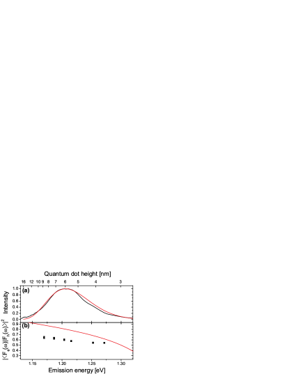
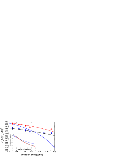
Using the experimental data on both the QD height distribution function, the emission spectrum, and the frequency dependence of the wavefunction overlap, we explore experimentally realistic parameters in order to match our experimental data. The first approach is to use the measured QD height distribution of Fig. 2 and include both shear and hydrostatic strain. Using optimized parameters corresponding to an aspect ratio of and an indium mole fraction of we find a very good agreement with the emission spectrum, as shown in Fig. 10(a). The electron-hole wavefunction overlap extracted from the radiative decay rate offers an additional test of this parameter set. In Fig. 10(b) the experimentally determined wavefunction overlap is plotted along with the resulting theory Joh . The theory predicts correctly that the wavefunction overlap decreases (increases) with emission energy (QD size), and the mechanism behind this effect is discussed in detail below. However, a clear systematic deviation between theory and experiment is observed, which turns out to be the case for all three strain models provided that the model parameters are constrained to optimally reproduce the measured spectrum. We conclude from this result that the measured height distribution of uncapped QDs is not very useful in determining the actual confinement volume of the overgrown QDs that the experiments are performed on. This is due to complex redistribution and intermixing processes of indium and gallium will occur during growth and subsequent regrowth Kegel et al. (2000); Liu et al. (2000), which are likely to modify the QD confinement potential and strain significantly.
Thus abandoning at this point the interpretation of the measured height distribution, which is closely related to the emission spectrum, we focus on the electron-hole wavefunction overlap. Keeping the aspect ratio fixed at a realistic value of and excluding for the moment the wetting layer, we obtain the overlap shown in Fig. 11. Here the only free parameter is the mole fraction of indium in the QD and the different strain models are compared. Note that the experimentally determined wavefunction overlap depends on , since it enters through the Kane energy, cf. Eq. (22). We find that including both shear and hydrostatic strain leads to a disagreement between experiment and theory. This demonstrates that the strain model developed for quantum wells fails in the case of QDs, which is sometimes assumed in the literature Li et al. (1996). Good agreement between experiment and theory can be obtained when including only hydrostatic strain or no strain at all for and , respectively. Judging from experiments available in the literature Liu et al. (2000); Kegel et al. (2000) both these values of are reasonable for overgrown QDs, so there is no support for favoring one of the two surviving strain models. We are led to the conclusion that in particular shear strain is less significant for QDs compared to quantum wells, although further microscopic details of QD composition and geometry would be required for a further investigation of these issues.
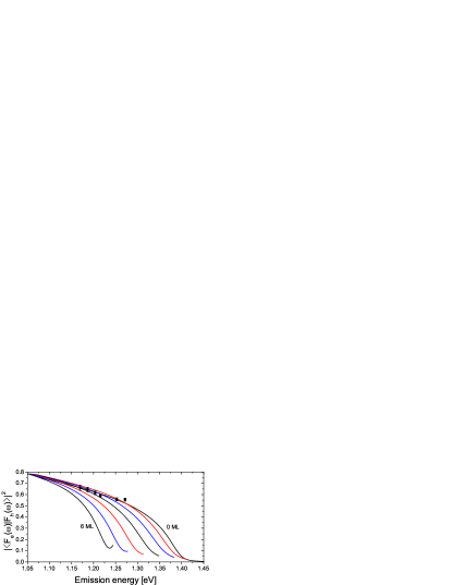
Figure 12 investigates the effect of the wetting layer thickness on the wavefunction overlap. In this case strain is omitted, the aspect ratio is , and the indium mole fraction . We find that for wetting layer thicknesses below 4 monolayer (ML) the wavefunction overlap is only slightly modified in the emission energy range of interest to the experiment. For a very thick wetting layer (6 ML), the QD wavefunction is modified such that the monotonic decrease of the wavefunction overlap with energy observed for all other thicknesses does not apply. This behavior can be understood as follows: for very thick wetting layers and small QDs a significant part of both the electron and hole wavefunctions are expelled from the QD giving rise to quantum well-like wetting layer states that can have an increased mutual overlap. For the QD sample of the experiment the wetting layer was on the order of 2 ML.
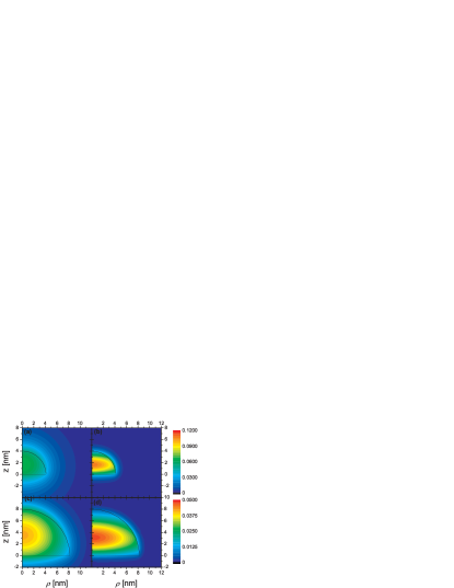
The above discussions point to a number of subtleties associated with a quantitative comparison between experiment and theory. These are mainly related to lack of knowledge about intrinsic properties of the QDs. Notably, the monotonic decrease in the electron-hole wavefunction overlap with emission energy is found to be a very general and robust result for a large range of different parameters. The generality of this result can be understood in a simple physical picture and is related to the differences in the electron and heavy hole effective masses. Thus, for any indium mole fraction, we have from Eqs. (32), (33), and (34) that and This in turn leads to a smaller Bohr radius for holes than for electrons, i.e. the hole wavefunctions are more compressible than the electron wavefunctions. Increasing the emission energy corresponds to decreasing the QD size. The large QDs emitting at small energies have a relatively large electron-hole wavefunction overlap. Decreasing QD size (i.e. increasing emission energy) compresses the electron and hole wavefunctions, and since the quantum confinement effect influences the electron wavefunction more than the hole wavefunction, the wavefunction overlap is decreased. This effect is illustrated in Fig. 13 where the calculated electron and hole wavefunctions for two different QD sizes are plotted. It is clearly observed that a reduction in the QD height leads to a compression of the hole envelope wavefunction while the electron wavefunction extends further into the surrounding barrier.
VI Conclusion
We have presented time-resolved measurements of spontaneous emission from self-assembled QDs near a semiconductor-air interface. The interface leads to a modification of the LDOS, which can be calculated in an exact model without any adjustable parameters. The excellent agreement between theory and experiment enables separating radiative and non-radiative decay rates whereby they can be determined with unprecedented accuracy. We reviewed the theory behind the experiment by calculating the spontaneous emission radiative decay rate in a full quantum model in which spontaneous emission is described by Wigner-Weisskopf theory. The radiative decay rate is proportional to the projected LDOS, which was derived using a Green’s function formalism.
From our measurements of the radiative decay rate at different emission energies we extracted the frequency dependence of the overlap of the electron and hole envelope wavefunctions. The experimental data were compared to theory by solving numerically the Schrödinger equation for a QD potential including the effects of shear and hydrostatic strain. From this model the spontaneous emission spectrum, which is inhomogeneously broadened due to the different sizes of QDs making up the ensemble, and the electron-hole wavefunction overlap were derived. An attempt to model the emission spectrum using the QD height distribution obtained by AFM on uncapped QDs was unsuccessful leading to the conclusion that this height distribution does not properly reflect the microscopic confinement potential of overgrown QDs. Regarding the frequency dependence of the electron-hole wavefunction overlap, we found good agreement between experiment and theory with reasonable assumptions about QD size, geometry, strain, and wetting layer thickness assuming purely hydrostatic strain or no strain at all. In contrast, systematic deviations were found when including both shear and hydrostatic strain. Although the numerical model employed here is too simple to reflect the microscopic details of the QD geometry such as, e.g., indium-gallium intermixing, it reflects this simple physical picture very well. A more detailed comparison between experiment and theory is limited by the lack of experimental input on the QD structure at the atomic scale, which would be required to verify more sophisticated QD models.
We finally discussed how the striking frequency dependence of the radiative decay rate, and consequently of the electron-hole wavefunction overlap, can be understood in terms of a very simple physical picture: The heavy hole wavefunction is more compressible than the electron wavefunction due to the larger effective mass. A reduction in the QD size therefore leads to a further localization of the heavy hole wavefunction, while the electron wavefunction delocalizes into the surrounding barrier. This leads to a decrease in wavefunction overlap for increasing emission energy.
Quantitative comparison of the experimental data to theory was limited by the lack of detailed experimental input about the microscopic composition of the QDs. Combining the detailed optical experiments presented here with techniques to extract local material properties of QDs, e.g., by high resolution transmission electron microscopy (TEM), will be a very exciting future research direction that also will pinpoint the need for more involved theoretical models of the QDs. We believe that the technique presented here to directly access the light-matter coupling strength will have important applications regarding proper design and characterization of solid state quantum photonic devices.
Acknowledgements.
We wish to thank J. Højbjerg, A. Kreiner-Møller and J. E. Mortensen for valuable work on the numerical model and C.B. Sørensen for growth of the semiconductor material. We gratefully acknowledge the Danish Research Agency for financial support (projects FNU 272-05-0083, 272-06-0138 and FTP 274-07-0459).References
- Imamoglu et al. (1999) A. Imamoglu, D. D. Awschalom, G. Burkard, D. P. DiVincenzo, D. Loss, M. Sherwin, and A. Small, Phys. Rev. Lett. 83, 4204 (1999).
- Gérard et al. (1998) J. M. Gérard, B. Sermage, B. Gayral, B. Legrand, E. Costard, and V. Thierry-Mieg, Phys. Rev. Lett. 81, 1110 (1998).
- Reithmaier et al. (2004) J. P. Reithmaier, G. Sȩk, A. Löffler, C. Hofmann, S. Kuhn, S. Reitzenstein, L. V. Keldysh, V. D. Kulakovskii, T. L. Reinecke, and A. Forchel, Nature 432, 197 (2004).
- Yoshie et al. (2004) T. Yoshie, A. Scherer, J. Hendrickson, G. Khitrova, H. M. Gibbs, G. Rupper, C. Ell, O. B. Shchekin, and D. G. Deppe, Nature 432, 200 (2004).
- Kistner et al. (2008) C. Kistner, T. Heindel, C. Schneider, A. Rahimi-Iman, S. Reitzenstein, S. Höfling, and A. Forchel, Optics Express 16, 15006 (2008).
- Laucht et al. (2008) A. Laucht, F. Hofbauer, N. Hauke, J. Angele, S. Stobbe, M. Kaniber, G. Böhm, P. Lodahl, M. C. Amann, and J. J. Finley, arXiv:0810.3010v2 (2008).
- Michler et al. (2000) P. Michler, A. Kiraz, C. Becher, W. V. Schoenfeld, P. M. Petroff, L. Zhang, E. Hu, and A. Imamoglu, Science 290, 2282 (2000).
- Reitzenstein et al. (2008) S. Reitzenstein, T. Heindel, C. Kistner, A. Rahimi-Iman, C. Schneider, S. Höfling, and A. Forchel, Applied Physics Letters 93, 061104 (2008).
- Lodahl et al. (2004) P. Lodahl, A. Floris van Driel, I. S. Nikolaev, A. Irman, K. Overgaag, D. Vanmaekelbergh, and W. L. Vos, Nature 430, 654 (2004).
- Julsgaard et al. (2008) B. Julsgaard, J. Johansen, S. Stobbe, T. Stolberg-Rohr, T. Sünner, M. Kamp, A. Forchel, and P. Lodahl, Applied Physics Letters 93, 094102 (2008).
- Robert et al. (2002) I. Robert, E. Moreau, B. Gayral, J.-M. Gerard, and I. Abram, Physica E 13, 606 (2002).
- Brokmann et al. (2004) X. Brokmann, L. Coolen, M. Dahan, and J. P. Hermier, Physical Review Letters 93, 107403 (2004).
- Leistikow et al. (2009) M. D. Leistikow, J. Johansen, A. J. Kettelarij, P. Lodahl, and W. L. Vos, Physical Review B 79, 045301 (2009).
- Johansen et al. (2008a) J. Johansen, S. Stobbe, I. S. Nikolaev, T. Lund-Hansen, P. T. Kristensen, J. M. Hvam, W. L. Vos, and P. Lodahl, Physical Review B 77, 073303 (2008a).
- Purcell (1946) E. M. Purcell, Phys. Rev. 69, 681 (1946).
- Drexhage (1970) K. H. Drexhage, J. Lumin. 1,2, 693 (1970).
- Novotny and Hecht (2007) L. Novotny and B. Hecht, Principles of Nano-Optics (Cambridge University Press, 2007).
- Chuang (1995) S. L. Chuang, Physics of optoelectronic devices (Wiley, 1995).
- Chance et al. (1978) R. R. Chance, A. Prock, and R. Silbey, Adv. Chem. Phys. 37, 1 (1978).
- Birkedal et al. (2000) D. Birkedal, J. Bloch, J. Shah, L. N. Pfeiffer, and K. West, Appl. Phys. Lett. 77, 2201 (2000).
- Warburton et al. (1997) R. J. Warburton, C. S. Dürr, K. Karrai, J. P. Kotthaus, G. Medeiros-Ribeiro, and P. M. Petroff, Phys. Rev. Lett. 79, 5282 (1997).
- Silverman et al. (2003) K. L. Silverman, R. P. Mirin, S. T. Cundiff, and A. G. Norman, Appl. Phys. Lett. 82, 4552 (2003).
- Wang et al. (2004) C. F. Wang, A. Badolato, I. Wilson-Rae, P. M. Petroff, E. Hu, J. Urayama, and A. Imamoglu, Applied Physics Letters 85, 3423 (2004).
- Lakowicz (2006) J. Lakowicz, Principles of Fluorescense Spectroscopy (Springer, 2006).
- Johansen et al. (2008b) J. Johansen, B. Julsgaard, J. M. Hvam, and P. Lodahl, In preparation (2008b).
- Barford (1990) N. C. Barford, Experimental measurements: precision, error and truth (Wiley, 1990).
- Cortez et al. (2001) S. Cortez, O. Krebs, P. Voisin, and J.-M. Gérard, Phys. Rev. B 63, 233306 (2001).
- van Driel et al. (2005) A. F. van Driel, G. Allan, C. Delerue, P. Lodahl, W. L. Vos, and D. Vanmaekelbergh, Physical Review Letters 95, 236804 (2005).
- Hanamura (1988) E. Hanamura, Physical Review B 37, 1273 (1988).
- Melnik and Willatzen (2004) R. V. N. Melnik and M. Willatzen, Nanotechnology 15, 1 (2004).
- Markussen et al. (2006) T. Markussen, P. Kristensen, B. Tromborg, T. W. Berg, and J. Mørk, Phys. Rev. B 74, 195342 (2006).
- Kristensen et al. (2008) P. Kristensen, A. F. Koenderink, P. Lodahl, B. Tromborg, and J. Mørk, Optics Letters 33, 1557 (2008).
- Li et al. (1996) S. S. Li, J. B. Xia, Z. L. Yuan, Z. Y. Xu, W. Ge, X. R. Wang, Y. Wang, J. Wang, and L. L. Chang, Physical Review B 54, 11575 (1996).
- Haug and Koch (1994) H. Haug and S. W. Koch, Quantum Theory of the Optical and Electronic Properties of Semiconductors (World Scientific, 1994).
- Vats et al. (2002) N. Vats, S. John, and K. Busch, Phys. Rev. A 65, 043808 (2002).
- Loudon (2000) R. Loudon, The Quantum Theory of Light (Oxford University Press, 2000).
- Dung et al. (2000) H. T. Dung, L. Knöll, and D.-G. Welsch, Physical Review A 62, 053804 (2000).
- Paulus et al. (2000) M. Paulus, P. Gay-Balmaz, and O. J. F. Martin, Phys. Rev. E 62, 5797 (2000).
- Coldren and Corzine (1995) L. A. Coldren and S. W. Corzine, Diode lasers and photonic integrated circuits (Wiley, 1995).
- Davies (1998) J. H. Davies, The physics of low-dimensional semiconductors: An introduction (Cambridge University Press, 1998).
- Andreev and O’Reilly (2005) A. D. Andreev and E. P. O’Reilly, Applied Physics Letters 87, 213106 (2005).
- (42) Note that in Fig.3.B of Ref. [14] the theoretical curve plotted is mistakenly rather than .
- Kegel et al. (2000) I. Kegel, T. H. Metzger, A. Lorke, J. Peisl, J. Stangl, G. Bauer, J. M. García, and P. M. Petroff, Physical Review Letters 85, 1694 (2000).
- Liu et al. (2000) N. Liu, J. Tersoff, O. Baklenov, A. L. Holmes, Jr., and C. K. Shih, Physical Review Letters 84, 334 (2000).
- Stier et al. (1999) O. Stier, M. Grundmann, and D. Bimberg, Physical Review B 59, 5688 (1999).
- Vurgaftman et al. (2001) I. Vurgaftman, J. R. Meyer, and L. R. Ram-Mohan, Journal of Applied Physics 89, 5815 (2001).
- Chow and Koch (1999) W. W. Chow and S. W. Koch, Semiconductor-laser fundamentals (Springer, 1999).
Appendix A Influence of strain on excitons confined in quantum dots
| Quantity | Value for | Unit | Reference(s) | |
|---|---|---|---|---|
| Lattice constant | Å | Stier et al. (1999) | ||
| Band gap | Stier et al. (1999) | |||
| CB effective mass | Stier et al. (1999) | |||
| Luttinger parameter | Stier et al. (1999); Vurgaftman et al. (2001) | |||
| Luttinger parameter | Stier et al. (1999); Vurgaftman et al. (2001) | |||
| Luttinger parameter | Stier et al. (1999); Vurgaftman et al. (2001) | |||
| CB Hydrostatic def. pot. | Stier et al. (1999) | |||
| VB Hydrostatic def. pot. | Stier et al. (1999) | |||
| VB Shear def. pot. | Vurgaftman et al. (2001) | |||
| Elastic stiffness constant | Vurgaftman et al. (2001) | |||
| Elastic stiffness constant | Vurgaftman et al. (2001) | |||
| Static dielectric constant | Stier et al. (1999) | |||
| Kane Energy | Coldren and Corzine (1995); Vurgaftman et al. (2001) |
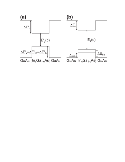
Strain due to the lattice constant mismatch between and is responsible for the formation of QDs during MBE growth in the Stranski-Krastranov growth mode. This means that the QDs are highly strained and this has significant impact on the electronic band structure. The interplay between geometry, chemical composition, and strain is complicated for QDs. During the growth, diffusion of and takes place, so that the resulting QD will consist of a significant fraction of even if it is grown by pure Kegel et al. (2000). Furthermore, it has been reported that is mainly concentrated in an inverted cone inside the QD giving rise to a complex strain profile Liu et al. (2000). Complete knowledge about such complex details is still lacking, and the purpose here is to introduce simple strain models and judge their validity by comparing to experimental data. We consider a lens-shaped QD with a lateral extension, which is larger than the extension in the growth direction. For this reason we approximate the strain of a QD by the model used in the case of a quantum well. This is further motivated by the fact that the QD is placed on top of a wetting layer, c.f. Fig. 9. The strain modifies the band offsets and energy gap of the QD, and the valence band degeneracy is lifted so that the transition with the lowest energy involves only heavy holes. This is illustrated in Fig. 14. We will assume that the bulk surrounding the QD is unstrained, however only heavy hole bands are included here as well since the influence of band mixing is minor in the barrier where the electron and hole wavefunctions are strongly damped.
One effect of strain is to shift the conduction and valence bands in energy. The strain describes the compression or expansion of the crystal lattice, which in general is described by a tensor . For biaxial strain, which describes the strain at planar heterojunctions, only the diagonal elements are relevant. We consider a thin layer of with lattice constant embedded in a barrier with lattice constant . We assume that all strain is incorporated in the layer and since the strain will be compressive. We have Chuang (1995)
| (23) |
where and are the elastic stiffness constants (matrix elements of the stiffness tensor). These strain components lead to a change in band structure and thus a modification of band energies and effective masses, as described by the Pikus-Bir strain model Chuang (1995). Biaxial strain can be decomposed into components of hydrostatic and shear strain. The hydrostatic compressive strain of the QD leads to a decrease of the band offsets exactly as for any hydrostatic compressive strain resulting from, e.g., a decrease of the temperature. For a thin strained epitaxial layer, the energy can be lowered by compensating the in-plane compressive strain by an expansion in the -direction (shear strain). We obtain the following heavy hole valence/conduction band offsets Chuang (1995)
| (24) | ||||
| (25) |
where
| (26) | ||||
| (27) | ||||
| (28) |
and we have introduced a number of quantities defined in Table 1. () is the unstrained conduction (valence) band offset which constitute () of the band gap difference between bulk and QD, so that, e.g., . The band gap of the strained QD is given by
| (29) |
where is the unstrained band gap of the material. These effects on the band structure are illustrated in Fig. 14.
Another important consequence of strain is that the effective heavy hole mass becomes highly anisotropic. In contrast the effective electron mass is not modified considerably since the conduction band is much more energetically isolated than the valence bands Chuang (1995); Vurgaftman et al. (2001). In our experiments the growth direction is parallel to the crystal axis, which is perpendicular to the wetting layer plane oriented along and directions. We will use and . Furthermore, since the crystal structure along the and axes are identical apart from a series of rotations, we have that .
The heavy hole masses for unstrained bulk are given by
| (30) | ||||
| (31) |
where , and are Luttinger parameters Vurgaftman et al. (2001). These are listed along with all other relevant QD material parameters for this work in Table 1. For , we have allowing for the axial approximation. Here and are replaced by their average value , leading to an isotropic heavy hole mass valid for unstrained bulk semiconductors Chow and Koch (1999)
| (32) |
These bulk effective masses are used to describe the barrier material surrounding the QDs. The strained heavy hole effective masses in the directions parallel with and perpendicular to the wetting layer plane are given by Chow and Koch (1999); Coldren and Corzine (1995); Chuang (1995)
| (33) | ||||
| (34) |
showing that the parallel component is strongly modified by strain.
Appendix B Numerical modeling of envelope wavefunctions
We solve the effective mass equation for electrons in the conduction band and holes in the valence band in order to calculate the overlap of the envelope wavefunctions. The effective mass equations describing the electron and the hole have the same form, but the effective hole mass anisotropy must be taken into account. We therefore consider the anisotropic valence band problem which has the isotropic conduction band problem as a special case. For both electrons and holes the effective mass depends on position due to the different effective masses in the QD and in the surrounding crystal matrix.
Using cylindrical coordinates and the axial approximation, the kinetic term in Eq. (2) reads
| (35) | ||||
Using separation of variables the effective mass Schrödinger equation can be written as
| (36) | ||||
The left and right hand sides of this equation are independent and they must therefore equal a constant, i.e. . The solution of this equation is which by the boundary condition implies that must be an integer. We are considering the ground state transition and therefore take . This leaves an equation describing the electronic motion in the -plane.
Eq. (36) is solved numerically after being reduced to a dimensionless form in order to avoid numerical issues related to the very small factors () appearing in this equation. We define the new dimensionless quantities through , , , , , and and furthermore take so that all spatial dimensions are measured in units of nanometer. By this transformation we obtain
| (37) | ||||
which is solved numerically using a finite element method.