Physical mechanisms of interface-mediated intervalley coupling in Si
Abstract
The conduction band degeneracy in Si is detrimental to quantum computing based on spin qubits, for which a nondegenerate ground orbital state is desirable. This degeneracy is lifted at an interface with an insulator, as the spatially abrupt change in the conduction band minimum leads to intervalley scattering. We present a theoretical study of the interface-induced valley splitting in Si that provides simple criteria for optimal fabrication parameters to maximize this splitting. Our work emphasizes the relevance of different interface-related properties to the valley splitting.
pacs:
03.67.Lx, 85.30.-z, 85.35.Gv, 71.55.CnSemiconductor nanostructures based on GaAs and Si Hanson et al. (2007); Lansbergen et al. (2008) are approaching the limit where device functionality relies on degrees of freedom of individual electrons. Recent progress in material processing allows precise controlled doping, band-structure engineering, and fabrication of high quality heterojunctions, which in turn pave the way for challenging applications such as the development of a scalable solid state quantum computer. The past few years witnessed tremendous experimental progress in the study of spin qubits at GaAs/AlGaAs quantum dots Hanson et al. (2007), which raises intriguing questions on the feasibility of spin qubits in Si quantum dot Friesen et al. (2003) or donor states Calderón et al. (2006) at a Si/barrier-material interface.
A clear advantage of spin qubits in Si over GaAs is the long spin coherence times in Si Das Sarma et al. (2004). On the other hand bulk Si conduction band edge is six-fold degenerate, a complication not present in GaAs. Near a (001) interface with a barrier material, this degeneracy is partially lifted, with the interface electron ground state remaining doubly degenerate. For electron spin qubits, the residual orbital degeneracy is an important spin decoherence source Tahan et al. (2002). This effect can be overcome if the ground state degeneracy is significantly lifted, which occurs close to an interface that can efficiently scatter carriers between the two degenerate valleys that are near opposite ends of the Brillouin zone Ando et al. (1982). Measurements of the doublet splitting, or valley splitting, present significant variations among different Si/barrier samples, ranging from to 1 meV gos . In this context, a simple physical model that can help identify the relevant fabrication-related parameters in order to maximize the valley splitting is a valuable tool in assisting current experimental efforts.
Theoretical approaches to describe the electronic behavior in the presence of an interface or heterojunction range from the effective mass approximation (EMA) Sham and Nakayama (1979); Friesen et al. (2007), tight-binding models gro to first-principles envelope function approach Foreman (2005). The present study, based on the physically motivated EMA Kohn (1957), aims to identify the relevance of sample-dependent parameters to the valley splitting. Our approach, while simple, is original and permits the study of the intervalley coupling due to a single interface, not employing periodic boundary conditions. The full plane wave expansions of the Bloch functions at the two conduction band minima obtained from ab initio calculations Koiller et al. (2004) contain relevant physical information about the underlying Si substrate, and are included explicitly. We identify physical mechanisms that control the coupling strength pointing to convenient choices for the barrier material and the interface quality. We also highlight advantages and limitations of the EMA, in particular the oscillations of the valley coupling with the arbitrary choice of the interface position within a single monolayer distance Sham and Nakayama (1979), which is an EMA artifact.
We consider the (001) Si/barrier system, so that the 6-valley Si bulk degeneracy breaks into a 2-valley ground state and a 4-valley excited state quartet to 30 meV above the ground doublet Kane (2000). We write the Hamiltonian for this problem as
| (1) |
where is the unperturbed bulk Si Hamiltonian. Translational symmetry is assumed in the plane, parallel to the interface, reducing the interface potential to a -dependent profile Bastard (1988). An electric field along the direction pushes the electron towards the interface. It is instructive to first consider an abrupt interface between Si and the barrier material; we model it here by taking in Eq. (1) to be a simple step potential Bastard (1988)
| (2) |
with representing the barrier height. The usual barrier material in Si devices are SiO2, corresponding to eV, and Si1-xGex alloys, in which case may be tuned by controlling the alloy composition. A typical value, for 0.2 to 0.3, would be meV.
Within single-valley EMA Kohn (1957), the lowest energy conduction band eigenfunctions for Eq. (1) are written as where are the Bloch wave vectors of the conduction band minima (). The envelope function satisfies the effective mass equation Bastard (1988)
| (3) |
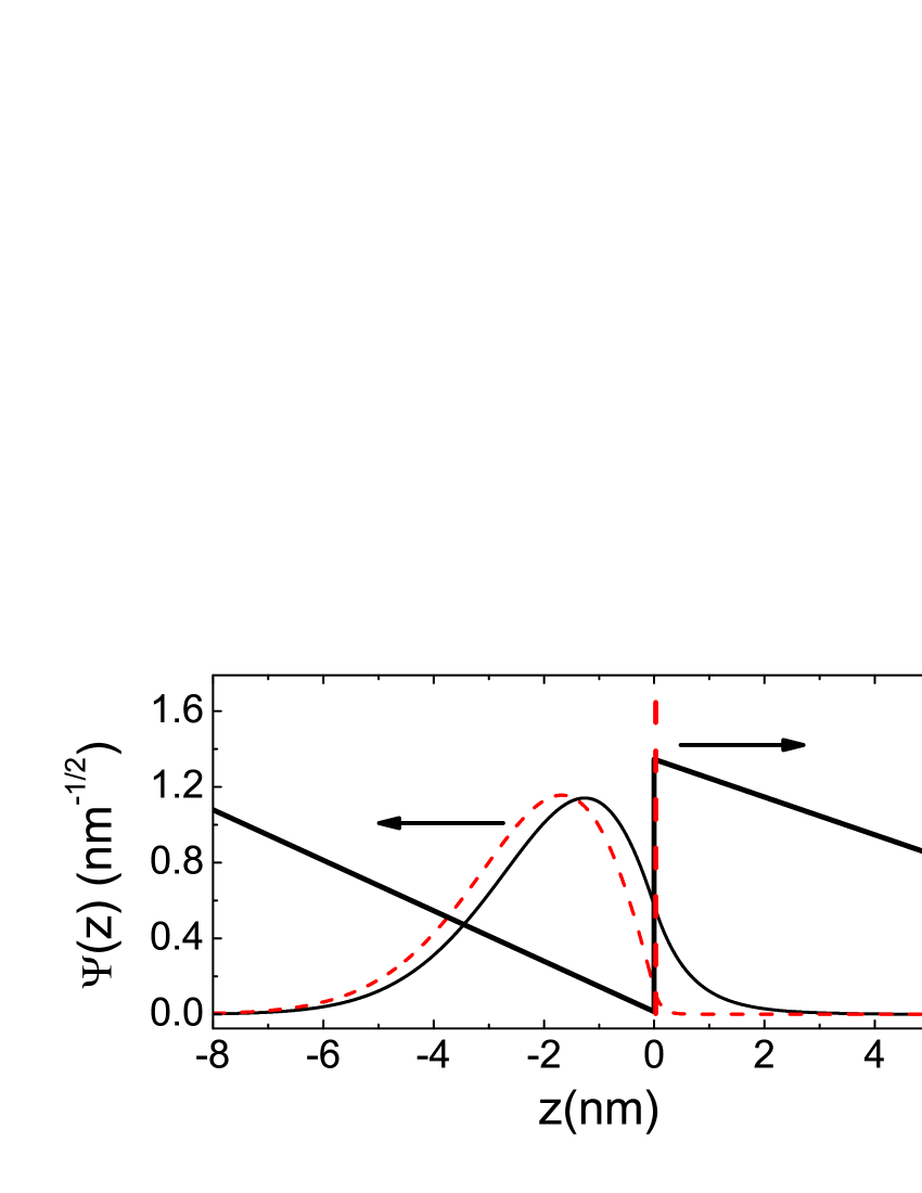
where is the longitudinal effective mass for Si. The ground state is numerically calculated through a finite differences method. Figure 1 gives solutions for the above values of . Strictly within the EMA assumption that the perturbation potential varies slowly in the length scale of the lattice parameter , the ground state would remain doubly degenerate, since one obtains equivalent solutions for . This assumption is clearly not valid in the case of the step potential in Eq. (2) which is discontinuous at the interface position , thus coupling the originally degenerate Bloch valley states . Also, the electric potential has a discontinuity in the derivative at due to the different values of the dielectric constant in the two materials. The interface position is initially taken to be .
Since are well separated in energy from the excited states, an effective low energy Hamiltonian is
| (4) |
where is the ground state energy obtained directly from Eq. (3), and the coupling due to the perturbation lifts the degeneracy leading to the valley splitting . The quantity of interest determining the splitting is , also called valley-orbit coupling, given here by , which is a complex number. Note that gives no contribution to this coupling. We write the periodic functions in terms of plane waves Koiller et al. (2004)
| (5) |
where are reciprocal lattice vectors. The expression for then reads
| (6) |
where the orthonormality of the and components is used, since there is no perturbation potential along these directions. The last term is an integral
| (7) |
with . Terms with and/or contribute to Eq. (6) with values comparable to the term alone. Integrating the contribution of the step potential by parts, Eq. (6) is rewritten as
| (8) |
Here, is the contribution from the of the form , similar to the effect of a -dependent function coupling potential. The contributions to , of the form , involve only the evanescent part of the envelope function penetrating into the barrier region. We find , the electric field potential contribution, to be negligible in all cases considered here, meaning that the “kink” in the electric field potential at the interface does not couple , thus following the standard EMA assumption. The role of the electric field in controlling is mainly to modify the envelope function .
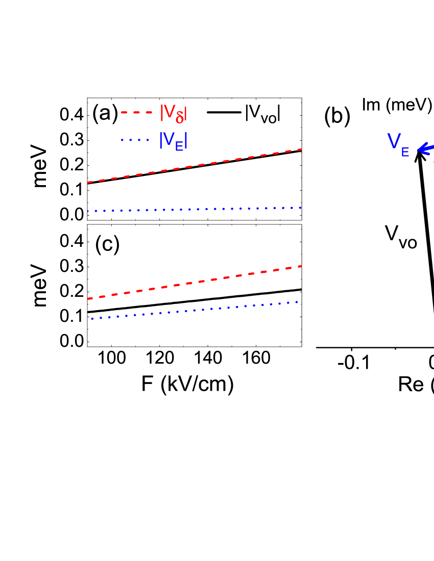
Fig. 2(a) shows the absolute value of the coupling, and of the and terms, for meV, as a function of applied field. In this case is well described by the -function contributions alone. If one is also interested in the eigenstates, the phase in becomes relevant and the contribution plays a role, as illustrated in Fig. 2(b). Fig. 2 (c) gives the results for the couplings dependence on the field for eV, and in this case both contributions affect . For the fields considered here, increases linearly with Sham and Nakayama (1979); Ando et al. (1982); gro .
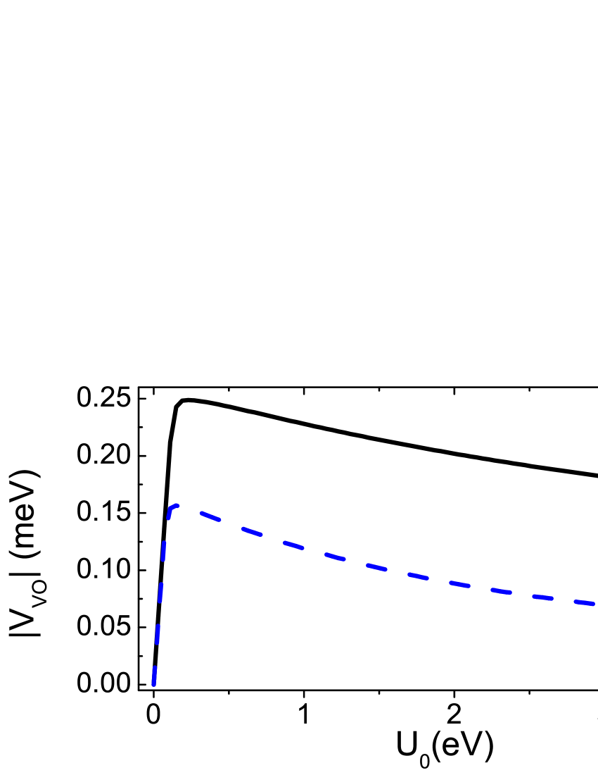
The expression for indicates that it is proportional to the product . As increases, decreases, so maximizing involves particular and not obvious conditions. The same is true for , for which only the evanescent tail of contributes. As shown in Fig. 1, when decreases the z-range that makes significant contribution to the integration increases. However, the highly oscillatory phases in the integrand usually suppress this contribution. A comparison of Fig. 2(a) and (c) shows that the larger actually produces a much larger , even though it corresponds to a more rapidly decaying evanescent envelope. Maximizing and independently does not necessarily maximize the absolute value of the complex sum . The net result is that may be similar in magnitude even for materials with a factor of 20 apart, as shown in Fig. 2. The general behavior of with the barrier height is illustrated in Fig. 3 (solid line) for kV/cm. As increases from 0, a sharp rise in is obtained up to a maximum coupling value around meV, followed by a slow decay: Very low or very high barriers tend to suppress the valley coupling. Tuning involves changing the alloy composition in the barrier, as in the case of Si1-xGex, or changing the barrier material. Such fabrication processes are in principle experimentally feasible.
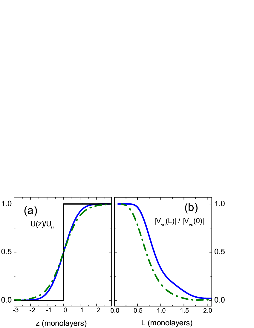
We now consider the effect of the interface width, which is disregarded in the step model. We use for in Eq. (1 interface models that are similar to previously measured and calculated profiles ste ), namely
| (9) | |||||
| (10) |
where is the complimentary error function. Both are characterized by a width , and reproduce for . They differ in the asymptotic behavior (respectively exponential and gaussian). The curves are very similar [see Fig, 4(a) for monolayer], as quantified by the RMS deviation with respect to the step potential; the RMS is only 8 larger than that of the profile. Yet, values of differ by a factor of two. This factor may be as large as 3 (for L1.3) with the same RMS ratio between the profiles. Fig. 4(b) gives the calculated coupling versus .
The interface width suppresses the intervalley coupling, as illustrated by the dashed lines in Fig. 3. The sensitivity of the coupling to the functional form of the interface potential for the same value of indicates that in real samples the coupling is strongly dependent on the type of interface disorder and roughness. Both effects contribute to the experimentally observed variation in the intervalley scattering among different samples.
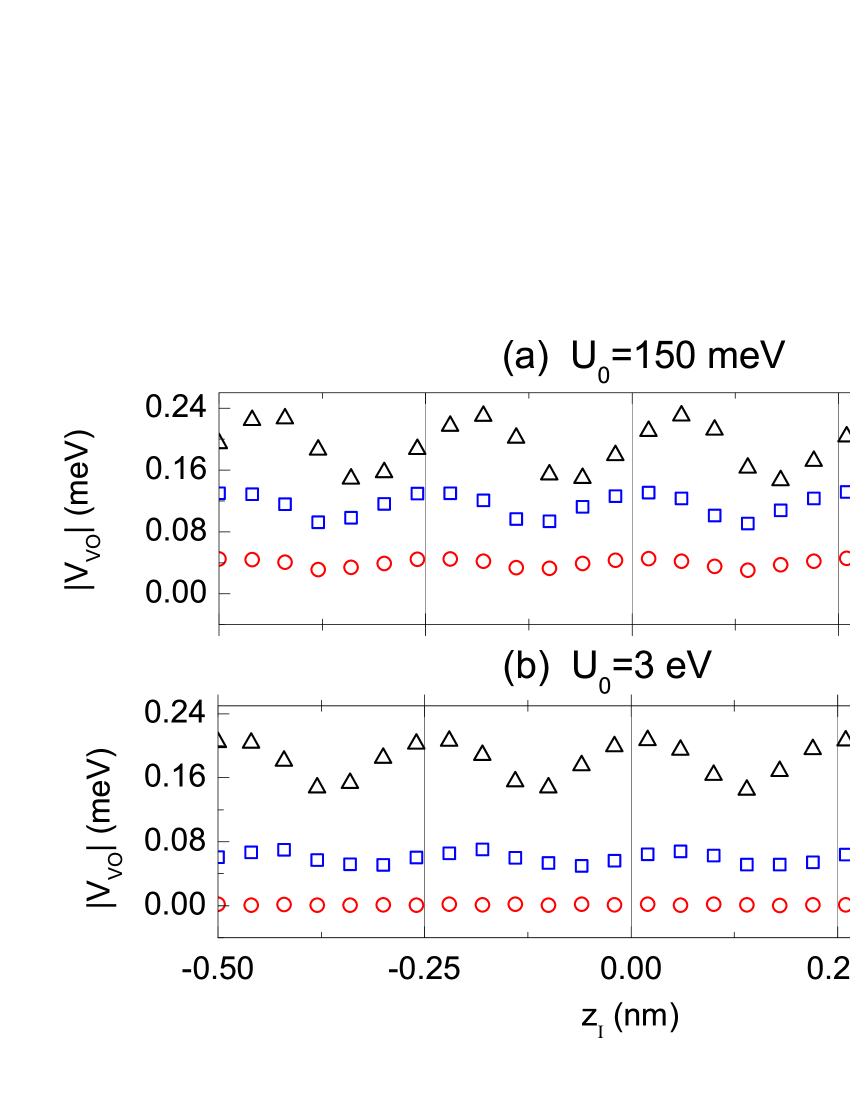
A fundamental limitation of the step potential is the sensitivity of the results to the interface position (taken to be 0 in the results presented so far) on a sub-monolayer length scale. This artifact, already obtained by Sham and Nakayama Sham and Nakayama (1979), is due to the periodic parts of the Bloch functions, which carry information about the underlying Si lattice and lead to different interference patterns due to the interface perturbation according to its location. As expected, shows oscillatory behavior with a 1 monolayer period, as seen in Fig. 5, but different models lead to different relative phases. The more physical model with a finite interface width partially overcomes this artifact, as the amplitude of the oscillations is reduced for finite . This is illustrated by the squares and circles in Fig. 5, and leads us to believe that a realistic model of the interface would largely remove this sensitivity to the exact interface location.
In summary, we have studied the conduction electron valley splitting in Si at a single Si/barrier interface using EMA. For a sharp interface, the simplicity of EMA allows us to identify two main contributions to the valley splitting: the electron wave function at the interface and the wave function gradient for the evanescent wave in the barrier material. We show that an external field (to increase the wave function at the interface) and an appropriate barrier potential height (through proper choice of barrier material) can help maximize the valley splitting.
A shortcoming of the sharp interface model is that its results are highly sensitive to the interface position. Taking into account the finite interface width reduces the sensitivity to the interface location while also reducing the intervalley scattering, because it blunts the sharp intervalley interference. This is illustrated by our result that steeper interfaces always favor larger intervalley splitting, while smoother profiles tend to reduce it, and may even lead to negligible coupling, as demonstrated by the profile in Fig. 5(b).
We do not expect our EMA results to be quantitatively accurate. Many effects are not included, such as strain, interface misorientation Friesen et al. (2007), atomic scale disorder, lateral confinement, or many-body corrections to the valley splitting. Nonetheless, the splittings on the order of 0.5 meV we obtained are in fair agreement with available measurements in Si/SiO2 and Si/SiGe interfaces gos .
In conclusion, we have calculated electron valley splitting in Si at a Si/barrier interface. We show that a sizeable single-particle splitting can be generated by applying a proper external field, choosing an optimal barrier material of a suitable potential height and producing sharp interfaces. Lateral confinement and many-body corrections can potentially further increase this splitting.
Acknowledgements.
We thank Rodrigo Capaz for helpful and fruitful discussions. This work was partially supported by the Brazilian agencies CNPq, FUJB, Millenium Institute on Nanotechnology - MCT, and FAPERJ. MJC acknowledges MAT2006-03741 and the Ramón y Cajal program (MICINN, Spain). XH and SDS thank financial support by NSA and LPS through US ARO, and by NSF.References
- Hanson et al. (2007) R. Hanson, L. P. Kouwenhoven, J. R. Petta, S. Tarucha, and L. M. K. Vandersypen, Rev. Mod. Phys. 79, 1217 (2007).
- Lansbergen et al. (2008) G. P. Lansbergen, R. Rahman, C. J. Wellard, I. Woo, J. Caro, N. Collaert, S. Biesemans, G. Klimeck, L. C. L. Hollenberg, and S. Rogge, Nat. Phys. 4, 656 (2008).
- Friesen et al. (2003) M. Friesen, P. Rugheimer, D. E. Savage, M. G. Legally, D. W. van der Weide, R. Joynt, and M. A. Eriksson, Phys. Rev. B 67, 121301 (2003).
- Calderón et al. (2006) M. J. Calderón, B. Koiller, X. Hu, and S. Das Sarma, Phys. Rev. Lett. 96, 096802 (2006).
- Das Sarma et al. (2004) S. Das Sarma, R. de Sousa, X. Hu, and B. Koiller, Solid State Commun. 133, 737 (2004).
- Tahan et al. (2002) C. Tahan, M. Friesen, and R. Joynt, Phys. Rev. B 66, 035314 (2002).
- Ando et al. (1982) T. Ando, A. Fowler, and F. Stern, Rev. Mod. Phys. 54, 437 (1982).
- (8) K. Takashina, A. Fujiwara, S. Horiguchi, Y. Takahashi and Y. Hirayama, Phys. Rev. B 69, 161304 (2004); S. Goswami, K. A. Slinker, M. Friesen, L. M. McGuire, J. L. Truitt, C. Tahan, L. J. Klein, J. O. Chu, P. M. Mooney, D. W. van der Weide, R. Joynt, S. N. Coppersmith and M. A. Eriksson, Nat. Phys. 3, 41 (2007).
- Sham and Nakayama (1979) L. Sham and M. Nakayama, Phys. Rev. B 20, 734 (1979).
- Friesen et al. (2007) M. Friesen, S. Chutia, C. Tahan, and S. N. Coppersmith, Phys. Rev. B 75, 115318 (2007).
- (11) G. Grosso, G. P. Parravicini, C. Piermarocchi, Phys. Rev. B 54, 16393 (1996); T. B. Boykin , G. Klimeck, M. Friesen, S. N. Coppersmith, P. von Allmen, F. Oyafuso and S. Lee, Phys. Rev. B 70, 165325 (2004).
- Foreman (2005) B. A. Foreman, Phys. Rev. B 72, 165345 (2005).
- Kohn (1957) W. Kohn, Solid State Physics Series, vol. 5 (Academic Press, 1957), edited by F. Seitz and D. Turnbull.
- Koiller et al. (2004) B. Koiller, R. B. Capaz, X. Hu, and S. Das Sarma, Phys. Rev. B 70, 115207 (2004).
- Kane (2000) B. E. Kane, Fortschr. Phys. 48, 1023 (2000).
- Bastard (1988) G. Bastard, Wave mechanics applied to semiconductor heterostructures (Halsted, New York, 1988).
- (17) F. Stern, Solid State Commun. 21,163 (1977); P. E. Batson, Journ. of Electron Microscopy 49, 267 (2000); T. Yamasaki, C. Kaneta, T. Uchiyama, T. Uda and K. Terakura, Phys. Rev. B 63, 115314 (2001).