Electrically Controlled Magnetic Memory and Programmable Logic based on Graphene/Ferromagnet Hybrid Structures
Abstract
It has been shown that the combining of the electrical effect on the exchange bias field with giant magneto-resistance effect of the graphene/ferromagnet hybrid structures reveals a new non-volatile magnetic random access memory device conception. In such device an electric bias realizes the writing bits instead a magnetic field of remote word line with high energy consumption. Interplay of two graphene mediated exchange bias fields applied to different sides of free ferromagnet results in programable logic operations that depends on specific realization of the structure.
pacs:
73.21.-b,85.75.-d,73.43.Qt,73.61.WpUp-today a magnetic field driving by the current of remote write line realizes the reversal of free ferromagnetic layer in a magnetic random access memory (MRAM). The giant magnetoresistance (GMR) effect is used to perform the reading in the storage stripe that is separated from word lines writing the bitsTang95 or integrated with reading channel.Melo97 Along with MRAM the programmable logic can be designed on basis of the GMR effect that utilizes high enough magnetic fields created by the current through a programming line.Black00 A programmable computing can be realized in such structures as a result of interplay between magnetic fields of input lines affected top and bottom ferromagnetic FM layers with different coercive fields.Ney03
Some advantage in device scaling has another mechanism of the MRAM switching based on spin transfer (or spin-torque)Slonczewski96 ; Berger96 in pillar structures.Katine00 ; Jiang04 It was demonstrated that spin-polarized current through the magnetic tunnel junction can drive the magnetic switching in nanoscale device.Fuchs04 Note that both aforementioned mechanisms of magnetization reversal need in high critical switching current and consequently high energy dissipation accompanied device operation. Design and creation of a composite free FM layer can result in reducing spin transfer currentMeng06 but it is not so radically that waives the problem of large energy consumption.
At the same time several mechanisms, which completely do not relate to electric current for magnetization reversal have been discussed in literature. Magnetization spontaneous reversal when a temperature variation modifies the exchange bias field in the magnetic heterostructures under the external magnetic field was reported in Ref.Li06 . Involving a multiferroic film to the magnetic structure brings about electrical control of exchange bias field, as it has been recently discussed in Ref.Bea08 . Very recently the authors showed that an atomic thin graphite (graphene) placed between two ferromagnetic dielectric layers (FDLs) realizes an indirect exchange interaction between them and this interaction can be easily controlled by applied electrical bias.SZKcondmat08 As this is a case, it raises a natural question: Can an graphene-incorporated structure accomplish the magnetization reversal of free FDL and how this effect can be utilized in MRAM and logic devices?
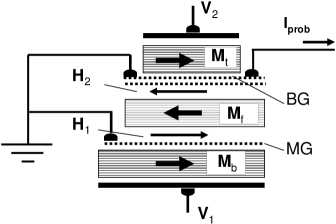
In present study we analysis a different approach to the problem of low-power-consuming non-volatile MRAM and logic design that based on the unique properties of the graphene placed in interface between two magnetic dielectric layers. In particular, the structure under consideration consists of a three ferromagnetic dielectric layers (FDLs) constructed from same material, which are coupled through monolayer graphene (MG) and bilayer graphene (BG) (Fig. 1). The magnetization of the bottom () and top () FDLs is pinned by strong enough coercivity or proximate antiferromagnets in the usual fashion.Nogues99 By technology reason they are assumed to be possessed the common direction along axis so that . The magnetization of the middle FDL can be controlled by exchange bias fields mediated by monolayer () and bilayer () graphenes if their sum exceeds the coercivity of free FDL.
The origin of the and stems from the exchange interactions and of graphene electrons with both pinned and free FDLs (coefficient is proportional to electron-magnetic ion exchange integral, is an electron spin). This establishes an indirect interaction through the graphene electrons in form of Zeeman energy ().SZKcondmat08
In very general way the thermodynamic potential of the graphene electrons interacted with both proximate FDLs determines the effective magnetic field . Straightforward calculations show that while the effective field projection on this direction is proportional to the modulation crest of the calculated for the electrons exchange interacted with proximate FDLs with parallel, , and antiparallel, magnetization. Finally it can be shownSZKcondmat08 that
| (1) |
where , is a total magnetic moment of the free FDL, and are its area and thickness. As in the case of conventional exchange bias, the strength of is inversely proportional to the thickness Nogues99 . This means that the influence of a back magnetic field generated by free DFL on the top and bottom magnetic layers can be strictly weaker their coercive fields under appropriate ferromagnetic layers widths.
The dependence of [Eq. (1)] on the electronic properties of the graphene layer leads to qualitatively different characteristics for MG and BG that the calculation of and highlights. In particular the carrier concentration (or position of the electro-chemical potential ) variation by impurity doping or/and the gate bias (, ; see Fig. 1) significantly influences exchange bias field in different manner for MG and BG.
Firstly, the signs of and are different in the wide range . While MG tends to establish parallel to (), BG favors the antiparallel alignment (). Secondly, a shift of from the graphene i-type point () affects the strengths of the exchange bias fields and in the opposite directions. Namely, the magnitude of gradually increases with or electron/hole concentration, whereas that of is at the maximum at with minimal free carrier concentration and decreases to zero when is large enough. The aforementioned characteristics can be captured by an expression in terms of dimensionless electron exchange energy ( eV) and the factor , which provides the specific dependence on for MLG () and BLG (),
| (2) |
where nm2 is the area of graphene primitive cells. Hereinafter the temperature assumes to be 300 K.
Figure 2 shows the , and their sum vs. evaluated at room temperature. As evident from the figure, the shift of can change the strength of by about a factor of two for both cases mediated by MG and BG. Moreover, the total field strength that controls the magnetization of free FDL varies with from negative maximal magnitude through zero to positive value of similar strength provided the equality for both MG and BG. The strength of hase been estimated at actual and as , where Oenm.SZKcondmat08 Such behavior inspires to use the joint action of and for electrical switching of free FDL between two stable states, which correspond to parallel or antiparallel to . By analogy with a magnetoresistive memory based on the ”spin-valve” effect,Melo97 ; Matsuyama97 we explore the coercivity that secures the stability of the magnetization with respect to quantum and thermal fluctuations. Apparently the strength of coercive magnetic field must be limited by inequality . Indeed, in such a case there is a range of exchange bias fields which, guarantees the reversal of magnetization while remains with former orientation.
The Fig. 2 also shows that the neutral charge point can correspond to the effective fields compensation, , if the equal impurity doping of MG and BG with magnitude has been achieved. Starting with this point, the total field can be variable in both directions by depletion of free carriers or their extra population with electro-chemical potential variation by applied electrical bias of both polarity. Hereinafter the properly impurity doping is assumed to be done for both graphene layers.
Once the problem of switching between two states and has been solved, it can be utilized in non-volatile memory provided different magnetic states of are surely discerned with graphene electrical properties. As it was recently shown, the conductivity of BG is characterized by significant sensitivity with respect to magnetic ordering of proximate FDLs because an misalignment of and results in bandgap opening and dispersion law flattering.SZK08 Other possibility consists in magnetic state detection through the MG electronic properties. As in the case of BG, one can expect the higher conductivity in parallel configuration than that in antiparallel orientation. This is because band spin splitting at makes a finite electronic density of states at any electron energy including Dirac point while this is not a case when graphene electrons do not experience spin splitting at . We calculate magnetoresistance of MG and compare it with that for BG at Fig.3. The figure indicates some advantage of BG with respect to magnetoresistance of MG that hase been depicted in device design (Fig. 1) with a BG reading line.
At large enough negative (Fig.4a) graphene-mediated field exceeds the and turns opposite to direction (Fig. 4b), i.e. their magnetization is antiparallel. Such configuration corresponds to large graphene resistance (Fig.4c).SZK08 Such a state remains since the electrical biases will switch off (Fig.4d). As soon as the chemical potentials of both graphene layers supplies the positive magnitude , the flips toward direction (Fig. 4b) so that parallel configuration of the and results in small graphene resistance (Fig.4c). Finally, the magnetoresistance reveals a hysteresis loop (Fig. 4d) with electro-chemical potential variation.
An evident advantage of the proposed concept consists in extremely low energy consumption since the graphene electrical recharging during the writing bit does not accompanied by high-density electric current. The intrinsic dissipation energy for each bit recording can be readily estimated in terms of the Eq. (2) as , where J/m2. Thus, the energy consumption around few J can be reached as soon as device will be scaling up to lateral sizes of hundred nanometers.
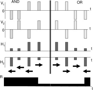
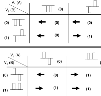
Another potentially useful properties of the device under consideration can be disclosed when one independently manipulates the chemical potentials of MG and/or BG. As a result, the interplay between MG exchange bias field and BG field will control the magnetic state of free FDL. In turn, this leads to realization of programmable logic operations AND or OR using and as the logic inputs and which correspond to be Boolean 0 (1) for negative (positive) voltage. We stress that the design of such logic device is same as the memory structure. Apparently, the output may be also a voltage related with the resistance of reading channel. We settle the correspondence of high (low) graphene resistance to 0 (1) output.
To demonstrate the device capability to logic operation, we start with antiparallel orientation (output 0) that can be established after negative pulses applied to both input, i. e. and . It can be readily show that any combination of the inputs with positive and negative pulses (or and ) generates the magnetic fields and which almost compensate each other, i.e. . Hence the output remains 0 for inputs , or , . The only input and gives rise constructive field interference that reverses free FDL in parallel configuration with output 1. (Fig. 5, left panel). Apparently, such input logicality corresponds to operation AND.
If we start with parallel orientation, , the output remains 1 under inputs , or , by same reason of destructive interference of and . The only input and reverses that gives rise output 0. (Fig. 5, right panel). Such input pulses logicality results in operation OR.
Fig. 6 recapitulates the programmable logic functioning. Note that the programming pulses precede each input signals, while the datum of logic operation is nonvolatile. Besides the estimation of energy consumption we provided for memory bit recording is applicable to logic as well. Thereby the logic functioning mediated by graphene possesses an advantage of low energy consumption compared with conventional programmable logic using giant magnetoresistance devices.Black00
In conclusion, we demonstrated that interference of the effective exchange bias fields mediated by the MG and BG enables to provoke the free FDL reversal under electrical bias manipulation. It was also shown that this effect conjointly with graphene giant magnetoresistance can be applied in memory as well as in programmable logic devices with record low energy consumption.
This work was supported in part by the US Army Research Office and the FCRP Center on Functional Engineered Nano Architectonics (FENA).
References
- (1) D. D. Tang, P. K. Wang, V. S. Speriosu, S. Le, K. K. Kung, IEEE Trans. Magn. 31, 3206, 1995.
- (2) L. V. Melo, L. M. Rodrigues, and P. P. Freitas, IEEE Trans. Magn. 33, 3295, 1997.
- (3) W. C. Black and B. Das, J. Appl. Phys. 87, 6674 (2000).
- (4) A. Ney, C. Pampuch, R. Koch, and K. H. Ploog, Nature 425, 485 (2003).
- (5) J. C. Slonczewski, J. Magn. Magn. Mater. 159, L1 (1996).
- (6) L. Berger, Phys. Rev. B 54, 9353 (1996).
- (7) J. A. Katine, F. J. Albert, R. A. Buhrman, E. M. Myers, and D. C. Ralph, Phys. Rev. Lett. 89, 3149 (2000).
- (8) Y. Jiang, S. Abe, T. Ochiai, T. Nozaki, A. Hirohata, N. Tezuka, and K. Inomara, Phys. Rev. Lett. 92, 167204 (2004).
- (9) G. D. Fuchs, N. C. Emley, I. N. Krivorotov, P. M. Braganca, E. M. Ryan, S. I. Kiselev, J. C. Sankey, D. C. Ralph, and R. A. Burhman, Appl. Phys. Lett. 85, 1205 (2004).
- (10) H. Meng and J.-P. Wang, Appl. Phys. Lett. 89, 152509 (2006).
- (11) Z. P. Li, J. Eisenmenger, C. W. Miller, and I. K. Schuller, Phys. Rev. Lett. 96, 137201 (2006).
- (12) H. Béa, M. Bibes, F. Ott, B. Dupé, X.-H. Zhu, S. Petit, S. Fusil, C. Deranlot, K. Bouzehouane, and A. Bartélémy, Phys. Rev. Lett. 100, 017204 (2008).
- (13) Y. G. Semenov, J. M. Zavada, and K. W. Kim, Phys. Rev. Lett. 101, 147206 (2008).
- (14) J. Nogués and I. K. Schuller, J. Magn. Magn. Mater. 192, 203 (1999).
- (15) Y. G. Semenov, J. M. Zavada, and K. W. Kim, Phys. Rev. B 77, 235415 (2008).
- (16) K. Matsuyama, H. Asada, S. Ikeda, and K. Taniguchi, IEEE Trans. Magn. 33, 3283 (1997).