Shot noise suppression in quasi-one dimensional Field Effect Transistors
Abstract
We present a novel method for the evaluation of shot noise in quasi one-dimensional field-effect transistors, such as those based on carbon nanotubes and silicon nanowires. The method is derived by using a statistical approach within the second quantization formalism and allows to include both the effects of Pauli exclusion and Coulomb repulsion among charge carriers. In this way it extends Landauer-Büttiker approach by explicitly including the effect of Coulomb repulsion on noise. We implement the method through the self-consistent solution of the 3D Poisson and transport equations within the non-equilibrium Green’s function framework and a Monte Carlo procedure for populating injected electron states. We show that the combined effect of Pauli and Coulomb interactions reduces shot noise in strong inversion down to 23% of the full shot noise for a gate overdrive of 0.4 V, and that neglecting the effect of Coulomb repulsion would lead to an overestimation of noise up to 180%.
Keywords - Shot noise, FETs, nanowire transistors, carbon nanotube transistors.
I Introduction
In the last few years, a huge collective effort has been directed to assess potential performance of quasi-1D Field Effect Transistors (FETs) based on Carbon Nanotubes [1, 2, 3] (CNTs), Silicon NanoWires [4] (SNWs), Graphene nanoribbons (GNRs) versus the International Technology Roadmap for Semiconductors [5] (ITRS) requirements, both from an experimental and a theoretical point of view. However, attention has been focused on electrical quantities like , subthreshold slope, mobility, transconductance [6, 7, 8], while an accurate investigation of electrical noise has been often neglected. Although the 1/f noise represents the major noise source affecting CNT-FETs performance [9, 10], the intrinsic shot noise is not only critical from an analog and digital design point of view, but can also provide relevant information regarding interactions among carriers [11] [12] [13], electron energy distribution [14] [15] and electron kinetics [16].
Due to the limited device dimensions, even in strong inversion only few electrons take part to transport, so that drain current fluctuations can heavily affect device electrical behavior. Pauli and Coulomb interactions play an important role in noise analysis, through fluctuations of the occupation number of injected states and fluctuations of the potential barrier along the channel.
From a numerical point of view, a self-consistent solution of the electrostatics and transport equations is mandatory in order to properly consider such effects. An analysis of this kind has been performed for example in double gate MOSFETs [17] and in nanoscale ballistic MOSFETs [18], where a strong shot noise suppression, mostly due to Pauli exclusion principle, has been observed.
A different approach, based on quantum trajectories within the De Broglie-Bohm framework has been instead presented in [19], where resonant tunneling diodes have been studied and heavy approximations have been adopted in order to easily consider electron-electron correlation in the many-body problem.
Actually, a complete understanding of the mechanism of suppression of shot noise in CNT and SNW-FETs is still a debated issue. Indeed, the significant suppression of current fluctuations by more than a factor 100 obtained at low temperature for suspended ropes 0.4 m long of single wall carbon nanotubes [20] has not been supported by a comprehensive theoretical analysis. Recent experiments of shot noise in CNT-based Fabry Perot interferometers [21] show that by only including Pauli exclusion one is able to explain most of the dependence of shot noise on the backgate bias, but in some bias conditions additional mechanisms of electron-electron interaction might be needed to explain the observed noise suppression. Theoretical efforts have been mainly addressed to model the electrical noise in SNW-FETs, where, within a scattering approach with the limitation of excluding space-charge effects on electron transmission, Pauli exclusion reduces electrical noise in strong inversion down to 0.6% of the full value for a gate overdrive of 0.3 V [22], whereas an interesting increase of noise is observed by including electron-phonon scattering processes [23].
Here, we present a new method to compute the shot noise power spectral density in ballistic CNT and SNW-FETs based on Monte Carlo (MC) simulations of randomly injected electrons from the reservoirs. In order to consider correlations between fermions, an analytical formula for the noise power spectral density has been computed by means of a statistical approach within the second quantization formalism. The derived formula has then been implemented in the self-consistent solution of the 3D Poisson and Schrödinger equations, within the NEGF formalism.
II Theory
The average current in a mesoscopic conductor can be expressed by means of Landauer’s formula:
| (1) |
where is the transmission amplitude matrix for states emitted from the source (S) and collected at the drain (D) and and are the Fermi-Dirac statistics of the S and D, respectively.
The zero-frequency noise power spectral density for a two-terminal conductor - the so-called Landauer-Büttiker noise formula - reads [24] [25]:
where is the conjugate transpose of the matrix . However, eq. (II) holds only if one assumes that fluctuations of the potential profile do not occur, i.e. that Coulomb interaction between carriers is completely neglected. Actually, the potential barrier along the channel fluctuates in time, since randomly injected electrons modify the height of the barrier through long-range Coulomb interaction, which in turn affects carriers transmission and eventually leads to the suppression of the drain current fluctuations.
In order to compute the expression of the power spectral density in the general case, we take advantage of the second quantization formalism. In particular, at zero magnetic field, the time-dependent current operator at the source can be expressed as the difference between the occupation numbers of carriers moving inward and outward the source contact in each quantum channel [24] ( and , respectively):
| (3) |
where
| (4) |
The operators and create and annihilate, respectively, incident electrons in the source lead with total energy in the transverse channel . In the same way, the creation and annihilation operators refer to electrons in the source lead for outgoing states. For the CNT case, the channel index runs over all the transverse modes and different spin, whereas for SNW, it also runs along the six minima of the conduction band in the space. In addition, the operators and are related through the unitary transformation
| (5) |
where the scattering matrix has dimensions and and are the number of quantum channels in the source and drain contacts, respectively. In the following, time dependence will be neglected, since we are interested to the zero frequency case.
If is a many-particle (antisymmetrical) state, the occupation number in the reservoir () in the channel can be either 0 or 1, and can be expressed as . Since we are interested to current fluctuations, we need to consider an ensemble of many electrons states and to compute statistical averages . By assuming no correlations between states at different energy or injected from different reservoirs, the statistical average of reads
| (6) |
In the following, we identify with . By means of (5), we obtain the mean current:
| (7) | |||||
where is the drain-to-source transmission amplitude matrix [26] . Since , and exploiting the unitarity of the scattering matrix, the mean squared current fluctuation for unit of energy can be expressed as:
where is defined as
and is the reflection amplitude matrix [26]. is our energy step of choice, i.e. the minimum energy separation between injected states.
Eq. (II) is expressed as the sum of four terms: the first, the second and the third terms correspond to the partition noise contribution. In particular, the first term is strictly related on the quantum uncertainty of the transmission process and disappears in the classical limit; the second term is associated to the correlation between transmitted states coming from the same reservoir; the third term to the correlation between transmitted and reflected states in the source lead; the minus sign in the second and third terms is due to exchange pairings, because of the fermionic nature of the electrons. In particular, the second and the third terms provide physical insights on exchange interference effects [27]. Finally, the last term represents the injection noise obtained as the variance computed on the ensemble of current samples.
According to the Milatz Theorem [28], the noise power spectral density in the zero frequency limit can be computed as , where is the injection rate, which can be expressed as:
| (12) |
Eventually, the power spectral density of shot noise at zero frequency can be expressed as:
| (13) |
It is worth noticing that eqs. (13) and (II) are not equivalent to the Landauer-Büttiker’s formula (II), since in eq. (II) the transmission (, ) and reflection () matrix are expressed as functionals of the statistics of the occupation of injected states from both contacts. In this way we are able to consider the fluctuation in time of the conduction and valence band edge profiles produced by the random injection through long-range Coulomb repulsion, providing a further source of noise suppression not included in eq. (II).
Indeed, from an analitical point of view, eqs. (II) and (13) reduce to eq. (II) when transmission and reflection do not depend, through Coulomb interaction, on random occupation numbers of injected states: in that case we can take the terms related to transmission and reflection out of the statistical averages in (II). By means of (6) and exploiting , the fourth term in (II) becomes:
| (14) | |||||
since at zero magnetic field . The terms , and are the Kronecker delta. Taking advantage of , becomes:
which is Landauer-Büttiker’s formula (II).
Let us now point out that eq. (13) would also simplify when identical and independent injected modes from the reservoirs are considered. In this case, , and are all diagonal, so that the second term in (II) becomes negligible. By exploiting the reversal time symmetry (, where is the transpose of ) and the unitarity of the scattering matrix, the power spectral density becomes:
III Simulation Methodology
In order to properly include the effect of Coulomb interaction, we self-consistently solve the 3D Poisson equation imposing Dirichlet boundary conditions in correspondence of the metal gates, and null Neumann boundary conditions on the ungated surfaces which define the 3D domain. Within a self-consistent scheme, the 3D Poisson equation is coupled with the Schrödinger equation with open boundary conditions, within the Non-Equilibrium Green’s function (NEGF) formalism which has been implemented in our in-house open source simulator NanoTCAD ViDES [29]. In particular the 3D Poisson equation reads
| (17) |
where is the electrostatic potential, is the fixed charge which accounts ionized impurities in the doped regions, while is the charge density per unit volume
| (18) | |||||
where is the mid-gap potential, is the local density of states associated to channel injected from contact and is the 3D spatial coordinate.
From a numerical point of view, in order to model the stochastic injection of electrons from the contacts, a statistical simulation on an ensemble of random configurations of injected electron states from both contacts has been performed. In particular, we have uniformly discretized with step E the whole energy range of integration [equations (II) and (18)]. Each random injection configuration has been obtained by extracting a random number uniformly distributed between 0 and 1 for each state represented by energy , reservoir , and quantum channel . The state is occupied if is smaller than the Fermi Dirac factor, i.e. is 1 for , and 0 otherwise.
Self-consistent simulations for a given actual random statistics in the source and drain contacts have been then performed, and, at convergence, the transmission (, ) and reflection () matrix have been computed, obtaining an element of the ensemble. In particular, for an actual electron distribution in the contacts, the Schrödinger equation is solved in order to obtain the spatial charge distribution (18) along the channel. Then, the latter is included in eq. (17) and the electrostatic potential is then computed and, once convergence of the NEGF-Poisson iteration scheme is achieved, the scattering matrix is evaluated, and a new sample to be added to the noise ensemble is obtained. Finally, the power spectral density can be extracted by means of eqs. (II) and (13). From a computational point of view, we have verified that computed on a record of 500 samples, using the energy step 5 10-4 eV, represents a good tradeoff between computational cost and accuracy of results [30].
Let us mention the fact that our approach is based on a mean field approximation of the Coulomb interaction, and that therefore the exchange term is not included. In the following, we will refer to self-consistent (SC) simulations when the Poisson-Schrödinger equations are solved considering and in eq. (18), while we refer to self-consistent Monte Carlo simulations (SC-MC), when statistical simulations with random occupations and inserted in eq. (18) are used. SC-MC simulations of randomly injected electrons allow to consider both the effect of Pauli and Coulomb interaction on noise. As a test, we have verified that if we perform MC simulations, keeping the potential profile along the channel fixed and exploiting the one obtained by means of SC simulation, the noise power spectrum computed in this way reduces to the Landauer-Büttiker’s limit (II), as already proved in an analitical way (eq. (II)): we refer to such simulations as non-self consistent Monte Carlo simulations (non SC-MC).
IV Simulation Results
IV-A Considered devices
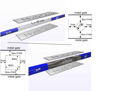
The simulated device structures are depicted in Fig. 1. We consider a (13,0) CNT embedded in SiO2 with oxide thickness equal to 1 nm, an undoped channel of 10 nm and n-doped CNT extensions 10 nm long, with a molar fraction . The SNWT has an oxide thickness equal to 1 nm and the channel length is 10 nm. The channel is undoped and the source and drain extensions (10 nm-long) are doped with cm-3. The device cross section is 44 nm2. A pz-orbital tight-binding Hamiltonian has been assumed for CNTs [31, 32], whereas an effective mass approximation has been considered for SNWTs [33, 34] by means of an adiabatic decoupling in a set of two-dimensional equations in the transversal plane and in a set of one-dimensional equations in the longitudinal direction for each 1D subband.
For both devices, we have developed a quantum fully ballistic transport model with semi-infinite extensions at their ends. A mode space approach has been adopted, since only the lowest subbands take part to transport: we have verified that four modes are enough to compute the mean current both in the ohmic and saturation region. All calculations have been performed at the temperature = 300 K.
IV-B DC Characteristics
In Fig. 2, the transfer characteristics for different drain-to-source biases computed performing SC and SC-MC simulations are plotted as a function of the gate overdrive in the logarithmic scale, both for CNT and SNW devices. In particular the threshold voltage for the CNT-FET at 0.05 V and 0.5 V is 0.43 V, whereas we obtain 0.13 V for 0.05 V and 0.5 V for the SNW-FET. As can be noted, SC and SC-MC simulations give practically the same results for CNT-FET, except in the subthreshold region where an interesting rectifying effect of the statistics emerges in the Monte Carlo simulations for a drain-to-source bias 0.5 V.
Instead, the rectifying effect is larger for SNW-FET, differences up to 30 % between the drain current computed by means of SC-MC and SC simulations can be also observed in the above threshold regime. In particular, for a gate voltage 0.5 V and a drain-to-source voltage 0.5 V, the drain current holds 2.42 10-5 A applying eq. (7), and 1.89 10-5 A applying Landauer’s formula (1). Current in the CNT-FET transfer characteristics increases for negative gate voltages due to the interband tunneling. Indeed, the larger the negative gate voltage, the higher the number of electrons that tunnel from bound states in the valence band to the drain, leaving positive charge in the channel, which eventually lowers the barrier and increases the off current [35].
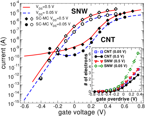
In the inset of Fig. 2 the average number of electrons inside the channel of a CNT and SNW-FET for two different biases 0.5 V and 0.05 V is shown. As can be seen, only very few electrons contribute to transport at any give instant, which requires us to attently evaluate the sensitivity of such devices to charge fluctuations: the smaller the drain-to-source voltage, the larger the average number of electrons in the channel, since, for low , carriers are injected from both contacts.
IV-C Noise
Let us now focus our attention on the Fano factor , defined as the ratio of the computed noise power spectral density and the full shot noise , . In Fig. 3, the Fano factor for both CNT-FETs and SNW-FETs is shown for = 0.5 V as a function of drain-to-source current .
Let us discuss separately the effects of Pauli exclusion alone and concurrent Pauli and Coulomb interactions. Triangles in Fig. 3 refer to computed by means of non SC-MC simulations on 104 samples, while diamonds to results obtained by means of Landauer-Büttiker’s formula, applying eq. (II). As expected the two approaches give the same results for both structures. Solid lines refer to computed by means of eqs. (II) and (13) and SC-MC simulations, i.e. Pauli and Coulomb interactions simultaneously taken into account.
In the sub-threshold regime ( 10-9 A), drain current noise is very close to the full shot noise, since electron-electron correlations are negligible due to the very small amount of mobile charge in the channel.
From the point of view of eq. (II), for energies larger than the top of the barrier, we have and the integrand in (II) reduces to . Instead, for energies smaller than the high potential profile along the channel, , so that we can neglect in (II), with respect to . Since , the integrand in (II) still reduces to . The Fano factor then becomes
| (19) |
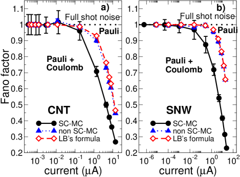
In the strong inversion regime instead ( 10-6 A), the noise is strongly suppressed with respect to the full shot value. In particular for a SNW-FET, at 2.4 10-5 A ( 0.4 V), combined Pauli and Coulomb interactions suppress shot noise down to 23 % of the full shot noise value, with a significant reduction with respect to the value predicted without including space charge effects as in Ref. [22], while for CNT-FET the Fano factor is equal to 0.27 at 1.4 10-5 A ( 0.3 V). Indeed, an injected electron tends to increase the potential barrier along the channel, leading to a reduction of the space charge and to a suppression of charge fluctuation. Note that, by only considering Pauli exclusion principle, we would overestimate shot noise by 180 % for SNWT ( 2.4 10-5 A) and by 70 % for CNT-FET ( 1.4 10-5 A).
IV-D Shot noise versus thermal channel noise
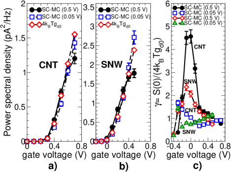
According to the classical approach for the formulation of drain current noise, channel noise is tipically described in terms of a “modified” thermal noise, as , where is the thermal noise power spectrum at zero drain-to-source bias , is the Boltzmann constant, is a correction parameter and is the source-to-drain conductance at zero .
Although the classical formulation accurately predicts drain current noise in long channel MOSFETs, where is equal to 1 in the ohmic region and 2/3 in saturation [28], it underestimates noise in short channel devices. In particular, experimental evidences [36] of an excess noise in short channel MOSFET have been explained in terms of the limited number of scattering events inside the channel which is uneffective in suppressing the non-equilibrium noise component [37], or in terms of a revised classical formulation by considering short channel effects, such as the carrier heating effect above the lattice temperature [38].
Actually, it can clearly be seen that non equilibrium transport easily provides and that the cause of is simply due to the fact that channel noise can be more properly interpreted as shot noise. For example, in the particular case of ballistic transport considered here, we can plot as as a function of the gate voltage in Fig. 4c. As can be seen, values of larger than 1 can be easily observed in weak and strong inversion. The strange behavior of as a function of the gate voltage is simply due to the fact that one uses an inadequate model (thermal noise) corrected with the parameter to describe a qualitatively different type of noise, i.e. shot noise.
IV-E Effect of scaling on noise
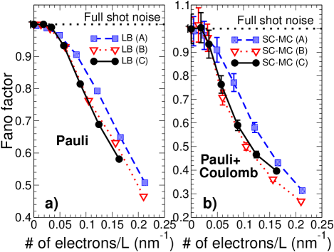
Let us now discuss the effect of scaling on noise, focusing our attention on a (13,0) CNT-FET. One would expect that an increase of the oxide thickness would reduce the screening induced by the metallic gate, so that the Coulomb interaction would be expected to produce a larger noise suppression. For example, in the limit of a multimode ballistic conductor without a gate contact, significantly suppression of about two order of magnitude with respect to the full shot value has been shown by Bulashenko et al [39].
However, Ref. [39] exploits a semiclassical approach assuming a large number of modes and the conservation of transversal momentum, i.e. the role of the transversal electric field induced by the gate voltage is completely neglected. In our case only four modes contribute to transport, while the top and bottom gates of the simulated devices partially screen the electrostatic repulsion induced by the space charge in the channel on each injected electron, so that a smaller noise suppression than the one achieved in Ref. [39] can be expected.
The Fano factor as a function of the average number of electrons inside the channel for unit length, computed by means of SC simulation and applying eq. (II), for three CNTs with different oxide thickness and channel length is shown in Fig. 5a: it shows results for CNT with = 1 nm, = 6 nm (A), CNT with = 1 nm, = 10 nm (B), and CNT with = 2 nm, = 10 nm (C). Fig. 5b shows the Fano factor computed by performing SC-MC simulations and applying eqs. (II) and (13). As can be seen, if the Fano factor is plotted as a function of the number of electrons per unit length, as in Fig. 5, curves are very close to one another, and effects of scaling are predictable.
V Conclusion
We have developed a novel and general approach to study shot noise in nanoscale quasi one-dimensional FETs, such as CNT-FETs and SNW-FETs. Our first important result is the derivation of an analytical formula for the noise power spectral density which exploits a statistical approach and the second quantization formalism. Our formula extends the validity of the Landauer-Buttiker noise formula [eq. (II)], to include also Coulomb repulsion among electrons. From a quantitative point of view, this is very important, since we show that by only using Landauer-Buttiker noise formula, one can overestimate shot noise by as much as 180%. The second important result is the implementation of the method in a computational code, based on the 3D self-consistent solution of Poisson and Schrödinger equation with the NEGF formalism, and on Monte Carlo simulations over a large ensemble of occurrencies, with random occupation of electronic states incoming from the reservoirs. As a final note, we show that scaling of ballistic onedimensional FETs is expected to weakly affect drain current fluctuations, even in the degenerate injection limit.
VI Acknowledgment
The work was supported in part by the EC Seventh Framework Program under the Network of Excellence NANOSIL (Contract 216171), and by the European Science Foundation EUROCORES Program Fundamentals of Nanoelectronics, through funds from CNR and the EC Sixth Framework Program, under project DEWINT (ContractERAS-CT-2003-980409).
References
- [1] R. Martel, T. Schmidt, H. R. Shea, T. Hertel, and Ph. Avouris. ”Single- and multi-wall carbon nanotube field-effect transistors”. Appl. Phys. Lett., vol. 73, pp. 2447–2449, 1998.
- [2] J. Guo, A. Javey, H. Dai, and M. Lundstrom. ”Performance analysis and design optimization of near ballistic carbon nanotube field-effect transistors”. IEDM Tech. Digest, ppp. 703–706, 2004.
- [3] N. Neophytou, S. Ahmed, and G. Klimeck. ”Non-equilibrium green’s function (NEGF) simulation of metallic carbon nanotubes including vacancy defects”. J. Comput. Electron., vol. 6, pp. 317–320, 2007.
- [4] Y. Cui, Z. Zhong, D. Wang, W. U. Wang, and C. M. Lieber. ”High performance silicon nanowire field effect transistors”. Nano Lett., vol. 3, pp. 149–152, 2003.
- [5] International Technology Roadmap for Semiconductors, URL http://public.itrs.net/.
- [6] T. D. Yuzvinsky, W. Mickelson, S. Aloni, G. E. Begtrup, A. Kis, and A. Zettl. ”Shrinking a Carbon Nanotube”. Nano Lett., vol. 6, pp. 2718–2722, 2006.
- [7] V. Perebeinos, J. Tersoff, and P. Avouris. ”Mobility in Semiconducting Carbon Nanotubes at Finite Carrier Density”. Nano Lett., vol. 6, pp. 205–208, 2006.
- [8] J. Knoch and J. Appenzeller. ”Tunneling phenomena in carbon nanotube field-effect transistors”. phys. stat. sol.(a), vol. 205, pp. 679–694, 2008.
- [9] Y. M. Lin, J. Appenzeller, J. Knoch, Z. Chen, and P. Avouris. ”Low-Frequency Current Fluctuations in Individual Semiconducting Single-Wall Carbon Nanotubes”. Nano Lett., vol. 6, pp. 930–936, 2006.
- [10] J. Appenzeller, Y.-M. Lin, J. Knoch, Z. Chen, and P. Avouris. ”1/f Noise in Carbon Nanotubes Devices-On the Impact of Contacts and Device Geometry”. IEEE Trans. on Nanotechnology, vol. 6, pp. 368–373, 2007.
- [11] G. Iannaccone, M. Macucci, and B. Pellegrini. ”Shot noise in resonant tunneling structures”. Phys. Rev. B, vol. 55, pp. 4539–4550, 1997.
- [12] G. Iannaccone, G. Lombardi, M. Macucci, and B. Pellegrini. ”Enhanced Shot Noise in Resonant Tunneling: Theory end Experiment”. Phys. Rev. Lett., vol. 80, pp. 1054–1057, 1998.
- [13] Ya. M. Blanter and M. Bütttiker. ”Transition from sub-Poissonian to super-Poissonian shot noise in resonant quantum wells”. Phys. Rev. B, vol. 59, pp. 10217, 1999.
- [14] T. Gramespacher and M. Büttiker. ”Local densities, distribution functions, and wave-function correlations for spatially resolved shot noise at nanocontacts”. Phys. Rev. B, vol. 60, pp. 2375, 1999.
- [15] O. M. Bulashenko and J. M. Rubí. ”Shot noise as a tool to probe an electron energy distribution”. Physica E, vol. 12, pp. 857, 2002.
- [16] R. Landauer. ”Condensed-matter physics: The noise is the signal”. Nature, vol. 392: pp. 58–659, 1998.
- [17] Y. Naveh, A. N. Korotkov, and K. K. Likharev. ”Shot-noise suppression in multimode ballistic Fermi conductors”. Phys. Rev. B, vol. 60, pp. R2169–R2172, 1999.
- [18] G. Iannaccone. ”Analytical and Numerical Investigation of Noise in Nanoscale Ballistic Field Effect Transistors”. J. Comput. Electron., vol. 3, pp. 199–202, 2004.
- [19] X. Oriols, A. Trois, and G. Blouin. ”Self-consistent simulation of quantum shot noise in nanoscale electron devices”. Appl. Phys. Lett., vol. 85, pp. 3596–3598, 2004.
- [20] P.-E. Roche, M. Kociak, S. Guéron, A. Kasumov, B. Reulet, and H. Bouchiat. ”Very low shot noise in carbon nanotubes”. Eur. Phys. J. B, vol. 28, pp. 217–222, 2002.
- [21] L. G. Herrmann, T. Delattre, P. Morfin, J.-M. Berroir, B. Placais, D. C. Glattli, and T. Kontos. ”Shot Noise in Fabry-Perot Interferometers Based on Carbon Nanotubes”. Phys. Rev. Lett., vol. 99, pp. 156804, 2007.
- [22] H. H. Park, S. Jin, Y. J. Park, and H. S. Min. ”Quantum simulation of noise in silicon nanowire transistors”. J. Appl. Phys., vol. 104, pp. 023708, 2008.
- [23] H. H. Park, S. Jin, Y. J. Park, and H. S. Min. ”Quantum simulation of noise in silicon nanowire transistors with electron-phonon interactions”. J. Appl. Phys., vol. 105, pp. 023712, 2009.
- [24] M. Büttiker. ”Scattering theory of current and intensity noise correlations in conductors and wave guides”. Phys. Rev. B, vol. 46, pp. 12485–12507, 1992.
- [25] Th. Martin and R. Landauer. ”Wave-packet approach to noise in multichannel mesoscopic systems”. Phys. Rev. B, vol. 45, pp. 1742–1755, 1992.
- [26] S. Datta. Electronic transport in mesoscopic systems. Cambridge University Press, 1995.
- [27] A. Betti, G. Fiori, and G. Iannaccone. ”Statistical theory of shot noise in quasi-1D Field Effect Transistors in the presence of electron-electron interaction”. http://arxiv.org/abs/0904.4274 (2009).
- [28] A. van der Ziel. Noise in Solid State Device and Circuits. Wiley, New York, pp. 16 and 75–78, 1986.
- [29] Code and Documentation can be found at the url: http://www.nanohub.org/tools/vides.
- [30] A. Betti, G. Fiori, and G. Iannaccone. ”Shot noise in quasi one-dimensional FETs”. IEDM Tech. Digest, pp. 185–188, 2008.
- [31] G. Fiori and G. Iannaccone. ”Coupled Mode Space Approach for the Simulation of Realistic Carbon Nanotube Field-Effect Transistors”. IEEE Trans. on Nanotechnology, vol. 6, pp. 475–479, 2007.
- [32] J. Guo, S. Datta, M. Lundstrom, and M. P. Anantam. ”Towards Multi-Scale Modeling of Carbon Nanotube Transistors”. Int. J. Multiscale Comput. Eng., vol. 2, pp. 257, 2004.
- [33] G. Fiori and G. Iannaccone. ”Three-dimensional simulation of one-dimensional transport in silicon nanowire transistors”. IEEE Trans. on Nanotechnology, vol. 6, pp. 524–529, 2007.
- [34] J. Wang, E. Polizzi, and M. Lundstrom. ”A three-dimensional quantum simulation of silicon nanowire transistors with the effective-mass approximation”. J. Appl. Phys., vol. 96, pp. 2192–2203, 2004.
- [35] G. Fiori, G. Iannaccone, and G. Klimeck. ”A three-dimensional simulation study of the performance of carbon nanotube field-effect transistors with doped reservoirs and realistic geometry”. IEEE Trans. Electron Devices, vol. 53, pp. 1782–1788, 2006.
- [36] A. A. Abidi. ”High-Frequency Noise Measurements on FET’s with Small Dimensions”. IEEE Transactions on electron devices, vol. 33, pp. 1801–1805, 1986.
- [37] R. Navid and R. W. Dutton. ”The physical phenomena responsible for excess noise in short-channel MOS devices”. IEDM Tech. Digest, pp. 75–78, 2002.
- [38] K. Han, H. Shin, and K. Lee. ”Analytical Drain Thermal Noise Current Model Valid for Deep Submicron MOSFETs”. IEEE Transactions on electron devices, vol. 51, pp. 261–269, 2004.
- [39] O. M. Bulashenko and J. M. Rubí. ”Shot-noise suppression by Fermi and Coulomb correlations in ballistic conductors”. Phys. Rev. B, vol. 64, pp. 045307, 2001.