Improving high-Tc dc-SQUID performance by junction asymmetry
Abstract
We study noise and noise energy of a high-Tc dc SQUID fabricated on a high- substrate whose conduction properties are given by transmission line physics. We show that transmission line resonances greatly enhance the noise. Remarkably, resistance asymmetry enhances these resonances even more. However, as the transfer function () scales the same way, the noise energy is reduced by asymmetry greatly enhancing the flexibility and performance of the SQUID.
1 Introduction
SQUIDs are versatile high-resolution magnetometers that find wide application in fields ranging from brain research, low-field MRI, geological prospecting, precision electrometry, detection of elementary particles and quantum computing. They are so powerful because of their large sensitivity and low intrinsic noise, leading to excellent signal-to-noise ratios that in some cases approach the limit set by quantum mechanics. High SQUIDs offer the possibility to be operated at temperatures of liquid nitrogen, lowering cost and enhancing flexibility. Their electrodynamics is more involved than that of their low- counterparts and optimization of signal-to-noise figures requires renewed attention.
In a previous paper [1], we have analytically studied transmission line resonances in high dc SQUIDS. Such resonances are exhibited in the characteristics of SQUIDs fabricated on substrates with high dielectric constant like strontium titanate. In [1], we analytically derived the SQUID power balance equation for both symmetric and asymmetric SQUIDs and investigated SQUID current-voltage , voltage-flux and voltage modulation characteristics. In this paper, we analytically study the effect of transmission line inductance on the noise characteristics of a dc SQUID. We will closely follow the methods used in [2].
The paper is organized as follows. In section 2, we set notations by describing the relevant circuit equations. In section 3, we study the effect of asymmetry on white noise in transmission line dc SQUIDs. We conclude in section 4. The calculational details are provided in appendix A. The SQUID parameters are the same as those used in [1].
2 Circuit equations
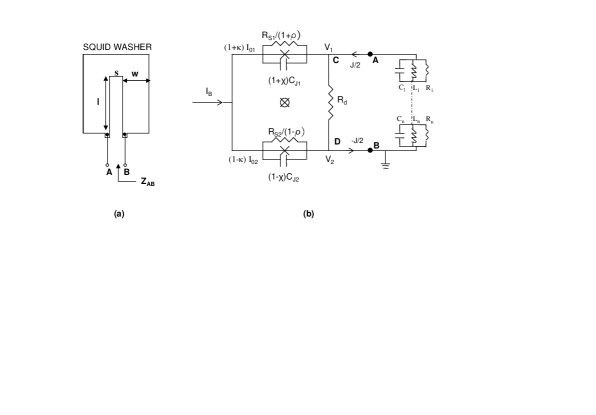
The geometry of the SQUID washer that we have used is shown in fig.(1a) [1]. This is a geometry commonly used to manufacture SQUIDs [3, 4, 5] and is the geometry Enpuku et al used to numerically investigate the effects of large dielectric constant of strontium titanate (STO) on the characteristics of high dc SQUIDs [6]. The slit of the SQUID washer makes up the SQUID inductance where , , and denote the slit length, slit width, electrode width and thickness of electrode respectively. For this geometry, the inductance per unit length of the slit and parasitic capacitance per unit length are given by [6, 7]:
| (1) |
where is the magnetic inductance per unit length and is the kinetic inductance per unit length of the SQUID slit given by[8]:
| (2) |
| (3) |
and
| (4) |
where is the permeability of free space, is the complete elliptic integral of the first kind [9] with a modulus is the penetration depth of the film, is the dielectric constant of the STO substrate and is the velocity of light in vacuum. The SQUID slit behaves as a transmission line with distributed inductance and distributed capacitance . The impedance of the slit seen from terminals A and B is given by [6]:
| (5) |
where is the characteristic impedance of the slit transmission line, is the angular frequency of measurement and is the junction parasitic inductance. The first term arises because the hairpin shaped slit can be treated as a shorted transmission line of length .
Now, using the formula [6]
| (6) |
eqn.(5) can be expanded as (in the lossless case with ):
| (7) |
with
and . This transformation to an equivalent circuit has the advantage that it allows us to consider loss in the transmission line. In the lossy case, the rf-loss is added to eqn.(7) leading to:
| (8) |
where and is a quality factor. Here is the SQUID slit length. This expression allows us to express the impedance by the series of L-C-R resonant circuits as shown in fig.(1b). The circuit equations can be easily derived by the application of Kirchhoff’s laws as in [1]. In fig.(1b), current entering point C should equal current leaving point C. We are assuming the most general case in which the SQUID is made up of junctions which are asymmetric [10, 12]. Here is the circulating current through the SQUID inductance, is the SQUID bias current, and are voltages across junctions 1 and 2 , and are the phases of junctions 2 and 1 and is a damping resistance in parallel to the SQUID inductance.
We write down the normalized circuit equations for the SQUID loop including random noise currents and . Let the average junction critical current be , the average junction normal state resistance be and the average junction capacitance be . Let the asymmetry parameter in be , that in be and that in be . So specifically, let us split [10] and . We normalize currents by , voltage by and time by . The ac Josephson relation gives , where is the normalized voltage and is the normalized time. Then including random noise currents and , the normalized circuit equations are:
| (9) |
| (10) |
Here, is the SQUID McCumber parameter with being the flux quantum and . In [1] the current-voltage characteristics in the absence of noise was derived. It was found to be
| (11) | |||||
Here , , and denotes the complex conjugate of . The phase difference between the two junctions have been set to where is the externally applied flux normalized to . Here,
| (12) |
| (13) |
| (14) |
and
| (15) |
If then should be replaced by in the calculations [1]. and are the SQUID inductance per unit length and SQUID parasitic capacitance per unit length respectively. The dielectric constant enters through . For more details the reader is referred to [1, 6].
3 White noise
We will now proceed to analyse the effect of noise with white power spectra, following closely the analysis in [2]. The calculation details are given in the appendix. The algebra is straightforward but very tedious. The final formula can be expressed as
| (16) |
Here and and can be extracted from (11). The noise power per unit angular frequency are given by
| (17) | |||||
| (18) |
with a noise parameter, is the Boltzmann constant and is the temperature. As in [2] we define the noise power spectra in practical units as
| (19) |
whose units are . In the lumped case limit, the expressions in [2] are reproduced. The explicit formula for and are rather unwieldy [13]. Since we are interested in small asymmetry, we only quote the expressions to leading order in with .
| (20) | |||||
| (21) |
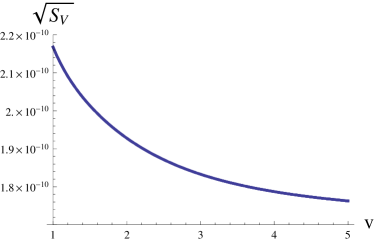
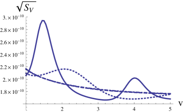
where are given in equations (13). We note that the capacitance asymmetry does not appear explicitly in the above formula although it is implicitly present in and . In figure 2(a), we show plots of SQUID voltage noise vs. bias voltage for different values of dielectric constant for both when the SQUID inductance is taken to be a lumped element and when it is taken to be a transmission line. The SQUID parameters are the same as those used in [1] i.e. , SQUID inductance, , SQUID parasitic inductance , and damping resistance . Figure 2(a) shows that in the lumped inductance limit, the noise curves overlap with each other. Thus the noise as a function of bias voltage is independent of substrate dielectric constant in this case. However in references [1, 6, 3], it has been shown that a high substrate dielectric constant can cause transmission line resonances in dc SQUID characteristics. Thus, in case of high SQUIDs, which are usually fabricated on STO substrates that are known to have a very high dielectric constant, it is important to model the SQUID inductance as a transmission line. In this case, we can see in figure 2(b), that the SQUID noise is definitely a function of dielectric constant and a high dielectric constant causes resonances to appear in the SQUID voltage noise vs. bias voltage curves at low voltages. This can be understood as follows. is maximum when is maximum. It follows from the analysis in [1] that this happens approximately at for positive integral . Since is inversely related to , it follows that for lower values for the first extremum in the noise occurs at higher . Resonances start appearing at voltage whenever the associated Josephson frequency matches the frequency of the lowest mode of the finite-length transmission line.
|
 |
|---|---|
| (a) | (b) |
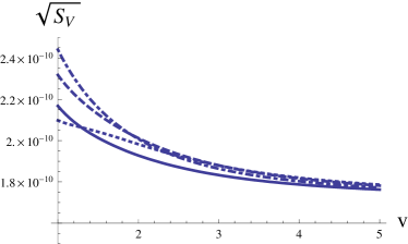
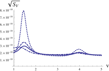
In figure 3, we show plots of SQUID voltage noise vs. bias voltage as a function of asymmetries in junction parameters. Here is used. Again we show both the lumped inductance limit as well the transmission line limit. We can see that in case of a lumped SQUID inductance, asymmetries in junction parameters do not affect the plots too much and one can say that presence of asymmetries leads to a marginal increase in noise as a function of bias voltage. However, when we consider the transmission line limit, asymmetries have a significant effect on the curves especially at resonance positions. asymmetry causes the sharpest increase. In our previous paper [1], we have seen that this is also the case for the vs. bias voltage curves. Thus asymmetry enhances the peak in both as well as voltage noise curves.
|
 |
|---|---|
| (a) | (b) |
This can be understood as follows: As we have explained in the previous section, the resistance asymmetry has been chosen such that the total resistance of the SQUID would be a constant if the SQUID inductance behaved as a lumped element as opposed to a transmission line. At positions off-resonance, the conductance through the transmission line is aided by the finite width of the resonant peaks. Thus off resonance, the same physics applies and the total off-resonant conductance of the SQUID remains constant. From the point of view of transmission line physics, the off-resonant conductance is proportional to the sum of the peak widths of the arms of the SQUID. On resonance, however, the conductance is proportional to the sum of “quality factors”, proportional to the inverse peak widths. This quantity increases as the asymmetry is increased. It needs to be emphasized that this is the asymmetry of the junctions, i.e., the loads of the transmission line and not asymmetries in the transmission lines themselves.
The effect is strongest for resistance asymmetry because it enters inversely into the quality factor. Critical current asymmetry enters through the Josephson inductance (). It is known that quality factor . Thus critical current asymmetry enters under the square root and thus has a much smaller influence. Also, both effects due to critical current asymmetry and resistance asymmetry counteract themselves.
Let us now briefly discuss the noise energy defined as [2, 11]
| (22) |
Remarkably, even though this asymmetry increases the absolute noise level, the noise energy is generally lowered by resistance asymmetry. This is seen in figure 4 a and b. As introduced above, the noise energy is the appropriately normalised performance quantifier, relating the absolute noise to the squared transfer function. As the transfer function shows the same enhancement by asymmetry just discussed but enters quadratically into the noise energy, the resistance asymmetry reduces the noise energy close to resonance and thus is rather smooth across the voltages of interest.

|
 |
|---|---|
| (a) | (b) |
4 Discussion
In this paper, we have studied the effect of asymmetry on the noise characteristics in high TC dc SQUIDs which behave as transmission lines. It was shown that asymmetry can be tuned to improve the signal to noise ratio. In particular, some resistance asymmetry can cause a marked decrease in noise energy both globally as well as at the resonance positions and hence, it is not necessary to strive for extreme symmetry between the junctions during device design.
Acknowledgments
US would like to acknowledge Ed Tarte for useful initial discussions. FKW acknowledges support from NSERC through a discovery grant. Research at Perimeter Institute is supported by the Government of Canada through Industry Canada and by the Province of Ontario through the Ministry of Research & Innovation. US and AS gratefully acknowledge IISc, Bangalore, India for hospitality during the last stages of this project.
Appendix A Calculation details
| (24) | |||||
Noise currents and have been combined to form the current noise and flux noise [2]
Let and satisfy equations (23) and (24) with i.e. in the absence of noise. In the following steps, we obtain an expression for a low-frequency component of the voltage in the presence of noise where is defined by . We consider the case where the noise current and the noise flux are small and express and as:
| (25) |
| (26) |
where and represent variations due to the noises and .
Substituting equations (25) and (26) into equations (23) and (24), we obtain the following linearized equations for and :
| (27) | |||||
with
| (29) |
| (30) |
where it is assumed that and . The trigonometric products in equations (29) and (30) have been expressed in a Fourier transform since the Josephson current has frequency components of in a finite voltage state of . Here, and are coefficients representing the magnitude of the harmonics and m is an integer. Since equations (27) and (A) are linear, one can consider independently solutions of and for individual frequency components of of and . Fourier transforms of and are defined as and respectively. The voltage noise is and its Fourier transform is . Therefore, the voltage noise power spectrum is given by [2] :
| (31) |
Next, we obtain the low-frequency component of the voltage noise, i.e. where the frequency is considered to be much lower then the Josephson oscillation frequency . It can be shown from equations 27 - 30 that the low frequency voltage noise arises not only from low-frequency components of and , but also from high frequency components of and . The voltage noise due to high frequency components of and has been expressed as the noise due to the Josephson mixing effect.
First, we obtain the value of due to the low frequency components of and . It is difficult to solve equations 27 and A exactly for frequency components of and . However, since the frequency is much lower than the Josephson oscillation frequency , one can regard and as quasi-static changes of and respectively. In this case, the value of should be given by the change of the dc voltage due to and , i.e.
| (32) |
where and are the dynamic resistance and the transfer function in the absence of noise respectively.
Next, we obtain the value of due to high frequency components of and i.e. with . In this regime, the R.H.S of equations (27) and (A) are much larger than the L.H.S. Thus as a first approximation to obtain the lowest order perturbation solution, the L.H.S are set to zero. Taking Fourier transforms of equations (27) and (A) then gives:
| (33) |
and
| (34) |
where,
with
and
Equations (33) and (34) are the zeroth order solutions. In order to get the first order solutions, we plug (33) and (34) into (27) and (A) L.H.S which gives expressions for and from (27), (A), (29), (30), (33) and (34). Now, . Therefore,
| (35) |
The expression for high frequency noise with the expressions for and substituted in (35) is quite long so we avoid writing the complete expression here. From (32) and (35) we get at the measurement frequency ,
| (36) |
References
References
- [1] Sinha U et al2008 Supercond.Sc. and Tech.21 (8)
- [2] Enpuku K et al1986 Journal of App. Phys.60 (12) 4218-23
- [3] Lee L P et al1995 App. Phys. Lett. 66 1539-41
- [4] Ludwig F et al1995 IEEE Tran. Appl.Supercond. 5 2919
- [5] Bar L R et al1995 Extended abstract ISEC ’95, Nagoya, Japan 322
- [6] Enpuku K et al1996 Journal of App. Phys. 80 (2) 1207-13
- [7] Yoshida K et al1992 Jpn.Journ.App.Phys. 31 3844
- [8] Ramo S et al1984 Fields and Waves in Communication Electronics (New York: John Wiley)
- [9] Gradshteyn I S and Ryzhik I M 2007 Table of Integrals, Series and Products (Academic Press)
- [10] Chesca B et al2004 SQUID handbook Chapter 2 ( Berlin: Wiley VCH)
- [11] SQUID handbook vol I ed. John Clarke and Alex Braginski.
- [12] Tarte E J et al2000 Supercond. Sc. and Tech. 13 1-6
- [13] The mathematica notebook for the noise calculation can be provided on request.