Ballistic Intrinsic Spin-Hall Effect in HgTe Nanostructures
Abstract
We report the first electrical manipulation and detection of the mesoscopic intrinsic spin-Hall
effect (ISHE) in semiconductors through non-local electrical measurement
in nano-scale H-shaped structures built on high mobility HgTe/HgCdTe quantum wells.
By controlling the strength of the spin-orbit splittings and the -type to -type
transition by a top-gate, we observe a large non-local resistance signal due to the ISHE in the
-regime, of the order of k, which is several orders of magnitude larger than in metals. In the
-regime, as predicted by theory, the signal is at least an order of magnitude smaller.
We verify our experimental observation by quantum transport
calculations which show quantitative agreement with the experiments.
I Introduction
Control, manipulation, and detection of spin polarized carriers are the focal goals of spintronics Awschalom and Flatté (2007). The creation of new technologies based on spin current manipulation requires new methods and materials for generating and controlling spin-based properties of active devices. While progress has been made in spin injection from a ferromagnetic metal into a semiconductor through tunneling barriers, its detection efficiency is still problematic. Applications of ferromagnetic semiconductors are challenged by their ferromagnetic transition temperatures which remain below room temperature. A clear avenue to circumvent several of these key problems is the direct use of electric fields to manipulate electron spins through spin-orbit coupling based effects in paramagnetic systems. Of these class of effects one of the premier candidate at present is the spin-Hall effect (SHE) Dyakonov and Perel (1971); Hirsch (1999); Hankiewicz and Vignale (2006); Engel et al. (2007); Murakami et al. (2003); Sinova et al. (2004) in which a transverse spin accumulation is created when an electric current is passed through a material with strong spin-orbit coupling, coming either from the band structure (intrinsic spin-Hall effect, ISHE) or from the scattering of electrons on heavy impurities (extrinsic spin-Hall effect, ESHE). Although the SHE has been very actively studied theoretically over the last few years Engel et al. (2007), experimentally only a few results have been reported due to the difficulty of detecting the effect. Early experiments demonstrating the effect utilized sensitive optical techniques Kato et al. (2004); Wunderlich et al. (2005); Sih et al. (2005). Electrical detection of the SHE, although much more desirable from the device point of view, is still more challenging and has been demonstrated only in metallic nanostructures metalSHE ; Weng08 The detected signals are weak, to a large extent due to the fact that samples are in the diffusive transport regime in mostly weak spin-orbit coupled systems. While most of the above experiments appear to result from an ESHE, the authors of Wunderlich et al. (2005) and Weng08 have attributed their observations the ISHE, involving the actual band structure spin-orbit coupling effects. A larger effect can be expected in samples where the transport is ballistic and unequivocally stems from the ISHE Hankiewicz et al. (2004); Nikolić et al. (2005). Such an experiment is the topic of this paper: we demonstrate electrical detection of the ballistic ISHE in high mobility HgTe-based nanostructures.
II Experimental setup
HgTe is a zero gap semiconductor which forms an inverted type-III QW with Hg0.3Cd0.7Te barriers when the well width is larger than 6.3 nm König et al. (2007). The two-dimensional electron gas (2DEG) in these structures exhibits a high carrier mobility (up to cm2/Vs Becker et al. (2007)) and a large, gate-controllable, Rashba-type spin-orbit splitting of up to 30 meV Gui et al. (2004); Hinz et al. (2006). The external top-gate also allows to change the carrier density from n-type through insulating to p-type regime. The samples studied in this paper contain a 8 nm wide symmetrically (Q2197) or asymmetrically (Q2198) -doped HgTe QW. The spacer width is 10 nm. A mean carrier mobility of cm2/Vs ( cm2/Vs) was deduced for an electron density of cm-2 ( cm-2) on an ungated Hall-bar of sample Q2197 (Q2198). From Shubnikov-de Haas measurements, we estimate that the mobility is ten times smaller in the p-type regime, which is mainly due to the larger effective mass.
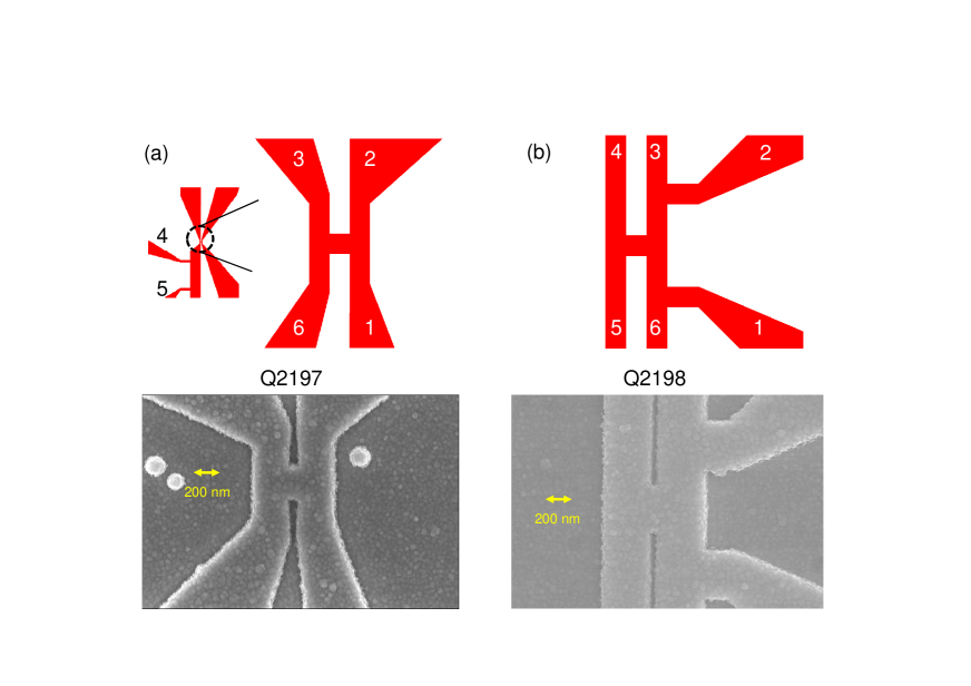
In order to electrically detect the ISHE, we have fabricated H-shaped mesa structures (see Fig. 1) using electron beam lithography and dry-etching techniques, following a design proposed previously by some of us in Ref. Hankiewicz et al. (2004). The Au/Ti electrode is deposited on top of a 110 nm thick SiO/SiN gate insulator layer which covers the entire sample. Ohmic contacts are fabricated by thermal In-bonding. Two additional contacts have been added to the H-structures to allow further characterization measurements. These contacts are attached to one leg either far away from (sample Q2197, Fig. 1a) or in close proximity to the H-bar (sample Q2198, Fig. 1b). The H-structures consist of legs 1 m long and 200 nm wide, while the connecting part is 200 nm wide and 200 nm long. [Note that the micrographs in Fig. 1 show the top gate, which masks the exact dimensions of the underlying H-mesa. Actually dimensions were verified from micrographs of adjacent mesa structures taken before gate deposition.] The estimated mean free path in these systems which establishes that the samples studied are well within the quasi-ballistic regime.
The idea of the transport measurements is as follows Hankiewicz et al. (2004). When an electric current flows in one of the legs of the H-bar structure (say between contacts 1 and 2 in Fig. 1a), a transverse spin current due to the intrinsic spin-Hall effect is induced in the connecting part. Subsequently, this spin current produces, due to the inverse spin-Hall effect Hankiewicz et al. (2005), a voltage difference in the opposite leg of the H-bar structure (in our example, between contacts 3 and 6) which can be measured by a voltmeter Hirsch (1999); Hankiewicz et al. (2004). The H-shape of the structure allows for a strong suppression of the residual voltage between contacts 3 and 6 that is directly due to the potential difference between contacts 1 and 2 and the actual ISHE signal can be easily identified by its dependence on the gate voltage. Experimentally, all measurements were performed using standard AC lock-in techniques, using an excitation voltage of 100 V at a sample temperature of 1.8 K.
III Experimental results
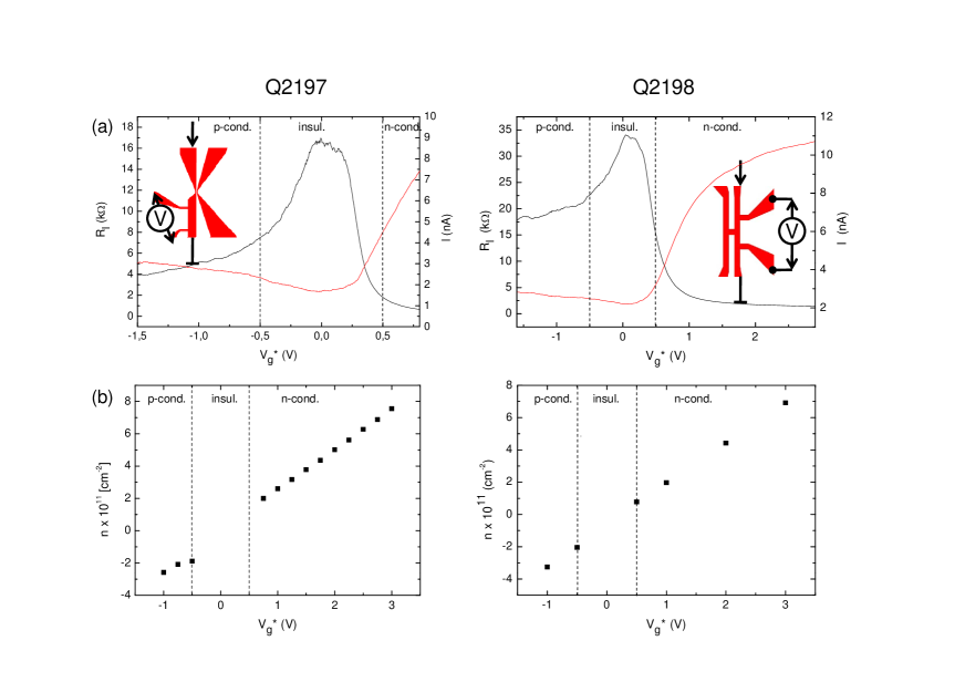
Fig. 2 (a) shows the gate voltage dependence of the sample current and the longitudinal resistance of samples Q2197 and Q2198. For reasons of comparison, we shift the gate voltage axis such that renormalized gate voltage V corresponds to the situation where the bulk Fermi level is in the center of the energy gap ( the actual voltages where = 0 V were V for Q2197 (Q2198), respectively). Fig.2 (b) shows the carrier density as a function of the renormalized gate voltage. This data was obtained through Hall-measurements on large Hall-bars fabricated from the same wafer and demonstrates that we can vary the carrier concentration enough to tune the sample from strongly -type ( cm-2), through the gap, down to a -type regime at V ( cm-2). For between -0.5 V and 0.5 V the samples are insulating (see Fig. 2).
We recently showed König et al. (2007) that the inverted band structure in HgTe quantum wells gives rise to the occurrence of the quantum spin Hall effect(QSHE), a novel type of quantum Hall effect that occurs at zero magnetic field, when the bulk of the sample is in the insulating regime. In samples that are smaller than the inelastic scattering length, the electrical conductance is then quantized at . Both the current and the resistance data on Q2197 and Q2198 [cf. Fig. 2 (a)] show indeed a resistance close to the conductance quantum when the gate voltage tunes the sample into the insulating regime ( V) [the deviation in Q2198 comes from the long voltage leads, see below]. As in the quantum Hall effect, QSHE quantization is caused by the formation of one-dimensional edge channels. The non-local character of carrier transport through these edge channels implies that the effect, which is much stronger than the signal anticipated for the ISHE in our samples, should also show up in our H-bar geometry. We have indeed observed very strong non-local QSHE signals in the course of our experiments on H-bars, and an extensive report of these results will be published elsewhere. For our present objective of an observation of the ISHE, however, the QSHE is an unwanted effect since it tends to swamp the ISHE signal - even though it shows its maximum at a different gate voltage.
The experiments shown in Figs. 3 represent two different approaches to suppress the non-local QSHE signal. One approach is to make the devices sufficiently small so as to provoke backscattering of the QSHE edge channels. Zhou et al. recently showed theoretically Zhou et al. (2008) that QSHE backscattering occurs when the wave functions for opposite spin channels overlap, and estimate that this happens for a device width of around 200-250 nm. This is the reason we report here on very narrow devices. The second method to suppress the QSHE is to choose a non-local configuration that implies edge channel transport over distances (much) longer than the inelastic length. This is the reason we have included the extra contacts on to the H-bar in Q2198: when the sample is insulating, the extra contacts force the edge channels to take a detour before entering the horizontal part of the H-bar.
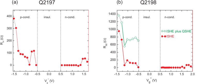
Figs. 3 (a) and (b) show the current and non-local resistance in a configuration suitable for picking up the ISHE signal as a function of applied gate voltage for both samples. The upper and lower panels show the results for an interchange of current and voltage contacts. One observes that for both samples the non-local signal strongly increases with gate voltage in the -regime. The non-local resistance is on the order of several 100 for sample Q2197 and larger than a k for sample Q2198. However, for the -type regime the signal is very low, does not show an appreciable dependence on gate voltage and thus can hardly be attributed to the ISHE. For sample Q2197, any non-local contribution of the QSHE edge channels is totally suppressed, so that we attribute the observed signal to the ISHE. The finite non-local resistance around for sample Q2198 is an indication that we have some residual non-local QSHE signal, possibly due to a slightly larger width of the horizontal bar. However, in the metallic regime, the significant increase of the non-local resistance signal can only be induced by the ISHE. For both samples, the strong non-local signal in the -regime remains almost unchanged even if the current and voltage contacts are exchanged. This is another strong argument that we observe the intrinsic spin-Hall effect.
IV Theoretical simulations
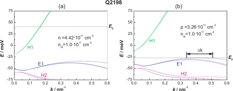
A key advantage of studying the ballistic ISHE is that methods to study the spin-dependent transport in this regime, e.g. the Landauer-Büttiker (LB) formalism, are well established and can give quantitative agreement with observed results, hence establishing a direct link between experiment and theoretical expectations. To model the specific devices studied in the experimental part, we first extract the effective masses and spin-orbit parameters from a series of band structure calculations Novik et al. (2005), where the influence of the top gate voltage is included in a self-consistent manner. We evaluate these parameters in the vicinity of the Fermi energy, since at low temperatures, the quantum transport can be described by propagating modes at the Fermi energy. Figs. 4 (a) and (b) show the calculated band structures for two representative carrier densities cm-2 and cm-2. For HgTe/HgCdTe quantum wells with an inverted band structure in the vicinity of , the conduction band (conventionally labeled H1 Novik et al. (2005)) has heavy-hole character while the valence band (E1) has electron-like character. However, hybridization of the energy states starts to play a role for and the spin-orbit splitting of both heavy hole and conduction bands must be considered in the form of a combination of linear and cubic terms. This is clearly relevant in our samples, because we find that the Fermi level passes through the H1 band around nm-1 for the n-type regime and through the E1 band around nm-1 for the p-type regime [see Fig. 4]. We find that the following Hamiltonian matches all important features emerging from the band structure calculations close to the Fermi level:
| (1) |
where for the -regime and for -type samples. and are the spin-orbit coupling parameters and in the -regime and for samples Q2197 and Q2198, respectively. In -regime , and for samples Q2197 and Q2198, respectively. is the disorder potential. The size of the structures used for the theoretical model is chosen in accordance with the actual dimensions of the experimental devices. In the experiments, the gate voltage causes changes in the spin-orbit splitting as well as in carrier density and as a consequence in the Fermi energy. We include this effect in the simulations by changing the carrier density with gate voltage according to the experimental data of Fig. 2 (b). The Fermi energies depend on the strength of the spin-orbit interaction and the carrier densities. To perform real-space LB calculations we rewrite the continuum effective mass Hamiltonian in a tight-binding form (shown in detail in the online appendix). In the tight-binding calculations, the disorder is calculated by randomly selecting the on-site energies in the range [], where , and is the transport scattering time calculated from the effective masses and the experimental mobility values. From the experimental mobility data, we find a corresponding disorder strength meV. For this value of , ten averages over disorder configurations are sufficient to obtain convergent results. The weak dependence of the observed effect on disorder in these materials is not surprising given that the disorder induced by short range scattering gives rise to vanishing vertex corrections Yang et al. (2008).
We work in the linear response regime and the voltages on different probes are found within the LB formalism using boundary conditions where a charge current of 10 nA, for the setup of structure Q2197, is driven between contacts 1 and 2, while between contacts 3 and 6 the electric current is zero. In this configuration the non-local resistance signal is . Details of calculations can be found in the online appendix and in Ref. Hankiewicz et al. (2004).
Figs. 5 (a,b) show the theoretical predictions for the non-local resistance signal as a function of gate voltage for samples Q2197 and Q2198, respectively. For sample Q2198, we included the theoretical prediction for the ISHE signal proper (closed circles) and the same, but adding a signal due to the QSHE (open circles). This QSHE signal has been taken directly from the experimental data, assuming that if suppression of the QSHE signal were complete, the non-local resistance signal should be zero in the insulating regime. Therefore, Fig. 5 (a) and Fig. 5 (b) can be directly compared with the experimental plots of Fig. 3 (a) and (b), respectively. Clearly, the theoretical results not only show a very similar behavior as the experimental resistance signal, but even have quantitative agreement. Furthermore, again in agreement with the experiment, the theoretically predicted signals are at least an order of magnitude stronger for the - than for the -regime. As in the experiment, we also find in the calculations that Q2198 exhibits a stronger signal than Q2197. This stems from the fact that for sample Q2198 the two extra voltage leads, used for suppressing the QSHE signal, in the metallic regime correspond to two extra contacts situated very close to the horizontal part of the H-bar. The oscillating character of both experimental and theoretical non-local resistance data stems from the fact that the ratio of the Fermi energy to the spin-orbit splitting changes over the range of gate voltage. In conclusion, our numerical calculations are in a very good agreement with the experimental results and confirm that the observed effect is indeed the ballistic ISHE.
V Summary
In conclusion, we have presented experimental data evincing the first observation of a ballistic ISHE in HgTe nanostructures, as well as simulations that firmly confirm this interpretation. We note that the effect measured is on order of a few % of the excitation voltage, which is due to the fact that our signal is of second order in the spin-order coupling, in that the spin current induced by the ISHE has to be turned into an electrical signal through the inverse SHE. Much larger effects can be anticipated for an experiment that shows a signal that is directly proportional to the spin Hall current. Such experiments are currently underway in our laboratory.
Acknowledgements.
We thank J. Schneider for assistance in the experiments, and C. Gould, S.-C. Zhang and X.-L. Qi for stimulating discussions. We gratefully acknowledge the financial support by the German-Israeli Foundation (I-881-138.7/2005), ONR under grant ONR-N000140610122, NSF under grant DMR-0547875, and SWAN-NRI. We thank Leibniz Rechenzentrum Münich for providing computer resources. J.S. is a Cottrell Scholar of the Research Foundation.References
- Awschalom and Flatté (2007) D. D. Awschalom and M. E. Flatté, Nature Physics 3, 153 (2007).
- Dyakonov and Perel (1971) M. I. Dyakonov and V. I. Perel, Phys. Lett. A 35, 459 (1971).
- Hirsch (1999) J. E. Hirsch, Phys. Rev. Lett. 83, 1834 (1999).
- Hankiewicz and Vignale (2006) E. M. Hankiewicz and G. Vignale, Phys. Rev. B 73, 115339 (2006).
- Engel et al. (2007) H.-A. Engel, E. I. Rashba, and B. I. Halperin, Handbook of Magnetism and Advanced Magnetic Materials (John Wiley & Sons Ltd, Chichester, UK, 2007).
- Murakami et al. (2003) S. Murakami, N. Nagaosa, and S.-C. Zhang, Science 301, 1348 (2003).
- Sinova et al. (2004) J. Sinova, D. Culcer, Q. Niu, N. A. Sinitsyn, T. Jungwirth, and A. H. MacDonald, Phys. Rev. Lett. 92, 126603 (2004).
- Kato et al. (2004) Y. K. Kato, R. C. Myers, A. C. Gossard, and D. D. Awschalom, Science 306, 1910 (2004).
- Wunderlich et al. (2005) J. Wunderlich, B. Kaestner, J. Sinova, and T. Jungwirth, Phys. Rev. Lett. 94, 047204 (2005).
- Sih et al. (2005) V. Sih, R. C. Myers, Y. K. Kato, W. H. Lau, A. C. Gossard, and D. D. Awschalom, Nature Physics 1, 31 (2005).
- (11) S. O. Valenzuela and M. Tinkham, Nature 442, 176 (2006); E. Saitoh, M. Ueda, H. Miyajima, and G. Tatara, Appl. Phys. Lett 88, 182509 (2006); T. Kimura, Y. Otani, T. Sato, Takahashi, and S. Maekawa, Phys. Rev. Lett 98, 156601 (2007); T. Seki, Y. Hasegawa, S. Mitani, S. Takahashi, H. Imamura, S. Maekawa, J. Nitta, and K. Takanashi, Nature Mat. 7, 125 (2008).
- (12) K. Weng, N. Chandrasekhar, C. Miniatura, and B.-G. Englert (2008), eprint cond-mat/00804.0096;
- Hankiewicz et al. (2004) E. M. Hankiewicz, L. W. Molenkamp, T. Jungwirth, and J. Sinova, Phys. Rev. B. 70, 241301 (2004).
- Nikolić et al. (2005) B. K. Nikolić, S. Souma, L. Zârbo, and J. Sinova, Phys. Rev. Lett. 95, 046601 (2005).
- König et al. (2007) M. König, S. Wiedmann, C. Brüne, A. Roth, H. Buhmann, L. W. Molenkamp, X.-L. Qi, and S.-C. Zhang, Science 318, 766 (2007).
- Becker et al. (2007) C. Becker, C. Brüne, M. Schäfer, A. Roth, H. Buhmann, and L. W. Molenkamp, Phys. Stat. Sol. (C) 4, 3382 (2007).
- Gui et al. (2004) Y. Gui, C. Becker, N. Dai, J. Liu, Z. Qiu, M. Schäfer, X. Shu, J. Chu, H. Buhmann, and L. W. Molenkamp, Phys. Rev. B 70, 115328 (2004).
- Hinz et al. (2006) J. Hinz, H. Buhmann, M. Schäfer, V. Hock, C. Becker, and L. W. Molenkamp, Semicond. Sci. Technol. 21, 501 (2006).
- Hankiewicz et al. (2005) E. M. Hankiewicz, J. Li, T. Jungwirth, Q. Niu, S.-Q. Shen, and J. Sinova, Phys. Rev. B 72, 155305 (2005).
- Zhou et al. (2008) B. Zhou, H.-Z. Lu, R.-L. Chu, S.-Q. Shen, and Q. Niu (2008), eprint cond-mat/0806.4810.
- Novik et al. (2005) E. Novik, A. Pfeuffer-Jeschke, T. Jungwirth, C. Becker, G. Landwehr, H. Buhmann, and L. W. Molenkamp, Phys. Rev. B 72, 35321 (2005).
- Yang et al. (2008) W. Yang, K. Chang, and S.-C. Zhang, Phys. Rev. Lett. 100, 056602 (2008).