Comprehensive Characterization of InGaAs/InP Avalanche Photodiodes at 1550 nm with an Active Quenching ASIC
Abstract
We present an active quenching application specific integrated circuit (ASIC), for use in conjunction with InGaAs/InP avalanche photodiodes (APDs), for 1550 nm single-photon detection. To evaluate its performance, we first compare its operation with that of standard quenching electronics. We then test 4 InGaAs/InP APDs using the ASIC, operating both in the free-running and gated modes, to study more general behavior. We investigate not only the standard parameters under different working conditions but also parameters such as charge persistence and quenching time. We also use the multiple trapping model to account for the afterpulsing behavior in the gated mode, and further propose a model to take account of the afterpulsing effects in the free-running mode. Our results clearly indicate that the performance of APDs with an on-chip quenching circuit significantly surpasses the conventional quenching electronics, and makes them suitable for practical applications, e.g., quantum cryptography.
Index Terms:
Avalanche photodiodes (APDs), SPAD, single-photon detection, telecom wavelengths, ASIC, quantum cryptography.I Introduction
Single-photon detectors are the key components in numerous photonics-related applications such as quantum cryptography [1], optical time domain reflectometry [2, 3] and integrated circuit testing [4]. We can classify single-photon detection into four classes: photomultiplier tubes [5]; semiconductor APDs [6, 7]; superconducting detectors [8]; and novel proposals such as using a single-electron transistor consisting of a semiconductor quantum dot [9]. In the telecommunication regime (1550 nm), InGaAs/InP APDs are currently the best choice for practical applications such as quantum cryptography [1] due to their favorable characteristics such as cost, size and robust operation with only thermo-electric cooling required.
To detect single photons, APDs must work in the so-called Geiger mode in which an inverse bias voltage (), exceeding the breakdown voltage (), is applied, such that even a single photoexcited carrier (electron-hole pair) can create a persistent avalanche and a subsequent macroscopic current pulse due to the process of impact ionization. After the avalanche, a passive or active quenching circuit [6], is used to reduce down to below , output a synchronized pulse and reset the APD for detecting the next photon.
InGaAs/InP APDs are currently fabricated with separate absorption, charge and multiplication layers [7] to ensure the lattice matching and preserve a low electric field in the InGaAs absorption layer with a narrower bandgap ( eV for In0.53Ga0.47As), minimizing the induced leakage currents, while a high electric field in the InP multiplication layer, enhancing the impact ionization effect. The middle charge layer can efficiently control the electric field profiles of the absorption and multiplication layers. The parameters of APDs are affected by many factors such as the crystalline quality of semiconductor device, imperfections of design and fabrication, quenching circuit, and operational conditions. Therefore, actual performance of these APDs is always compromised and optimized for different applications.
In the past decade efforts have been made to characterize and further improve APD performance on the single-photon level at 1550 nm [10, 11, 12, 13, 14, 15, 16, 17, 18, 19, 20, 21, 22]. Recently, integration of the quenching electronics for InGaAs/InP APDs to an ASIC [23, 24] has been implemented. The measured results on some key parameters of APDs demonstrate active quenching ASICs can efficiently improve the noise-efficiency performance, and it has been shown that these APDs can work in a free-running mode [24]. However, full characterization of APDs with the ASIC is still necessary to better understand the improvements they provided. In this paper, we fully test 4 InGaAs/InP APDs at 1550 nm with an active quenching ASIC operating both in the free-running and gated modes, and compare the improvements with conventional electronics.
II The setup and the principle of the ASIC
The schematic setup for testing APDs is shown in Fig. 1. A digital delay pulse generator (DG 535, Stanford Research Systems Inc.) provides synchronous signals for the whole system. One of its periodic outputs drives a 1550 nm laser diode (LD) to produce short optical pulses with ps FWHM. The optical pulses are split into two parts by a 10/90 asymmetric fiber beamsplitter (BS). 90% of the signal is monitored by a power meter (IQ 1100, EXFO Co.) to regulate the precise variable attenuator (Var. ATT, IQ 3100, EXFO Co.) in real-time and stabilize the intensity of the output from the attenuator that goes to the pigtailed APD. The pins of the APD and ASIC are soldered together on a small printed circuit board, while the body of APD is fixed on the top of 4-layer thermoelectric cooler and actively stabilized with a closed-loop control.
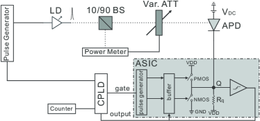
The schematic diagram of the ASIC, fabricated with a m complementary metal oxide semiconductor (CMOS) process, is shown in the gray area of Fig. 1. The amplitude of the gate signals from the complex programmable logic device (CPLD) is first converted to the power supply voltage VDD ( V) of the chip. Two pulses are then generated to control the PMOS and NMOS switches respectively which have extremely fast rise and fall times. There is a very short delay between the two control pulses to avoid the simultaneous conduction of the two switches. The timing is such that at the beginning of the gate the PMOS switch is closed while the NMOS switch is opened, to charge the voltage at the quenching point (Q) up to VDD, and then the PMOS switch is reopened. The total voltage difference between cathode and anode of the APD is VDD, exceeding for Geiger mode operation. The NMOS switch remains open until the end of the gate if no avalanche happens, or until the active quenching after a triggered avalanche. During the avalanche process, current across the APD rapidly increases and results in an increasing voltage drop across the resistor . The comparator and the following circuit quickly detects the the voltage drop at Q and immediately informs the buffer to close the NMOS switch to drop the voltage at Q to zero, and also generate a synchronous detection output to the CPLD. Normally the detector output maintains the high level until the falling edge of the next gate. Actually, when a detection is registered the CPLD inserts a short reset pulse after the gate, otherwise the CPLD does nothing. In the free-running mode, the gates from the CPLD are not used and VDD is applied to the cathode of the APD until an avalanche is excited. Further technical description about the ASIC can be found in Ref. [23].
III Performance tests of APDs
We have tested 4 commercial APDs: #1 (JDSU0131T1897); #2 (JDSU0122E1711); and #3 (Epitaxx9951E9559) from JDSU; as well as #4 (PLI-DOI61910-040W059-076) from Princeton Lightwave, Inc., and compared the different performance characterizations of these APDs with the ASIC quenching system.
III-A Integrated versus conventional quenching electronics
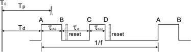
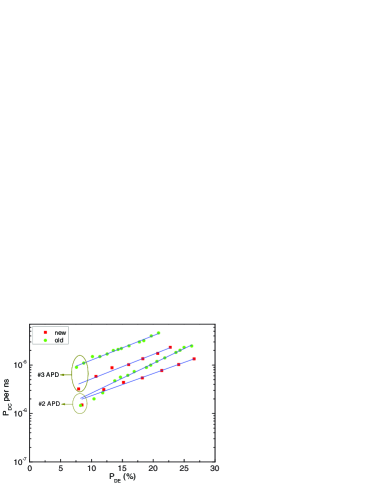
Firstly, we perform the key parameter measurements on the same (#3) APD using the new (ASIC) and old (conventional non-integrated circuit) [11, 14] quenching electronics under the same settings (T K ). Fig. 3 shows the comparison results for dark count ( per ns) vs single-photon detection efficiency () probabilities, afterpulse probability () and jitter, respectively. Using the double-gate method [14] (we discuss this in the latter section) as shown in Fig. 2, these parameters can be related to:
| (1) |
where (, ) is the observed dark count (afterpulse, detection) rate, () is the effective width of detection (afterpulse) gate in ns and is the mean photon number per optical pulse with repetition frequency of . During the experiment, the conditions are kHz, ns and , and these are fixed unless specifically mentioned in this paper.
The three curves manifestly exhibit the performance improvements provided by the new quenching electronics. The improvement of a factor of 3 in the - performance for #3 APD shown in Fig. 3a is better than expected. As we know, due to the ASIC the size of the electronics are greatly decreased and the electronic cables and the lengths of wires are reduced. This brings a lot of benefits such as superior signal integrity, minimized parasitic capacitance and reducing fake avalanche signals due to signal reflections or electronic noise. We also observe - performance improvements on other APDs, for instance, for #2 APD shown in Fig. 3a the ratio is always about 1 (no improvement) when and slowly increases to about 2 when . The - performance improvement ratio strongly depends on the APD devices and operational conditions. Although the reasons of the significant improvement for #3 APD are not clear yet, one possibility could be different gate heights and discrimination approaches between the two quenching systems, as it is the noise that is improved here, for a given excess bias voltage.
a)
b)
c)
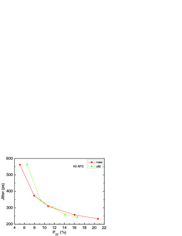
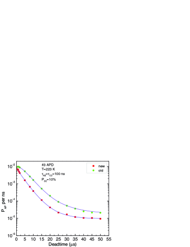
We see, in Fig. 3b, a significant improvement in the between the two cases as expected. The is generally proportional to the total number of carriers generated during an avalanche and hence motivates small and rapidly quenched avalanches. The results here clearly illustrate the circuit response and quenching time of the new system for the avalanche discrimination are faster than the old system. We will come back to this in more details in the following sections.
Timing jitter (time resolution) is another key parameter. It is defined as the temporal uncertainty of detection output for an avalanche with fixed arrival time of photons. Time jitter strongly depends on device fabrication and , corresponding to excess bias () on the APD. Larger can generate higher electric fields, which will shorten the trapping time of the carriers in the absorption and grading layers, and also the buildup time of avalanche, hence reducing the jitter. To measure this we use a time-correlated single photon counting (TCSPC) board (SPC-130, Becker & Hickl GmbH) with a time resolution of ps FWHM and minimum time slot of fs, to measure the jitter properties. A synchronized signal from a pulse generator is used as the TCSPC’s “stop” while the detection output signal is used as “start”. The measured jitter is the overall jitter of the system, including the jitter ( ps) and width ( ps) of arrived optical pulses, the APD’s intrinsic jitter owing to the stochastic process of carrier dynamics, as well as from the associated electronics. The jitter performance is shown in Fig. 3c and we only see a minor improvement when . We expect the electronic jitter to be slightly better as the ASIC can efficiently reduce the propagation time and jitter of the signals. At higher we don’t observe the improvement and the negligible difference between the two cases is due to contributions from the associated external electronics, e.g., CPLD and discriminator that are used with the new system but not the old one. However, varying degrees of improvement have been observed on other APDs even at higher .
III-B , and thermal activation energy
In order to illustrate the universal improvements afforded by this new quenching system, we use the new system operating in the gated mode to repeat the measurement on different APDs and temperature settings, as shown in Fig. 4 and Fig. 5.
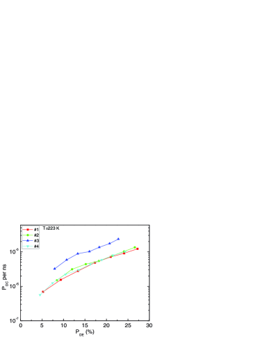
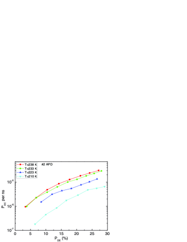
The - behavior of #1, #2 and #4 APDs are very similar, with ns-1 and at K, as shown in Fig. 4, but much better than #3 APD. Fig. 5 shows the behavior of #2 APD from K to K, and we see a reduction in to ns-1 for the same .
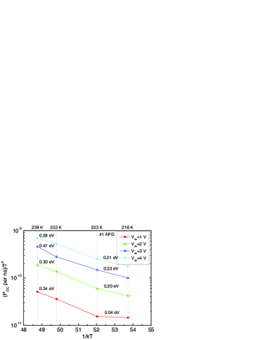
The origin of the dark counts is mainly due to the defect concentration in the semiconductor device. There are two main mechanisms for the generation of dark carriers: thermal generation; and tunneling generation. The thermal generation means that a carrier is transferred from the valence band to the conduction band either directly or via the midgap defects, owing to the thermal excitation. Tunneling generation means that a carrier tunnels between the two bands, or it is trapped by a defect first and then tunnels to the conduction band, which is also called trap-assisted tunneling (TAT) [21, 22]. Combinations of the two mechanisms are normally not taken into account. The simulations for m InGaAsP/InP APDs performed by Donnelly et al. [25] show that TAT in the multiplication layer dominates the at low temperature, while at high temperature the two mechanisms compete with each other. Unfortunately, the dark count model for nm InGaAs/InP APD is more complicated than this, though one can investigate the so-called thermal activation energy () to identify the dominant mechanism [19, 20, 21]. Theoretically, the relationship between , and temperature (T) can be expressed as [20]
| (2) |
where is the Boltzmann constant and (T) is a function of temperature with slow variations. In Fig. 6, four curves of versus T for #1 APD with different values are plotted. We evaluate the difference of values for two small temperature ranges ( K K and K K). The fitting values are displayed in Fig. 6. The results clearly show that generally higher temperatures induce larger values and suggest that the thermal generation mechanism around K dominates while the TAT mechanism is more significant around K, see also ref. [26].
III-C Afterpulsing
During an avalanche process, due to a photon detection, dark count effects, or afterpulsing itself, a carrier can be trapped by a defect in the multiplication layer. This carrier may excite another avalanche - an afterpulse, during subsequent gates. This process severely limits the APD performance for high frequency operation due to the need to apply long, typically 10 s, deadtimes where the APD is inactive. There are two methods to measure the behavior. The first approach measures the total noise behavior as a function of . When is large enough, say, s, the is negligible and the measured noise is primarily due to dark counts. After subtracting , the quantity of noise left can be attributed to afterpulsing. This method was used in Ref [24] but, while straightforward, generally overestimates .
The other approach, the double-gate method [14], as used in our setup is illustrated in Fig. 2. If there is a click during the detection (AB) gate, the CPLD will also generate an afterpulse (CD) gate after AB’s reset pulse with a delay of to the falling edge of the AB gate. This corresponds to the deadtime. The CPLD also generates a reset pulse for the CD gate only when an afterpulse detection is registered during this gate. This method directly measures .
Assuming a Poisson distribution, can be expressed as
| (3) |
where is the detrapping rate at time and is the avalanche probability. We use a multiple trapping model (multiple detrapping times) to describe [19, 20],
| (4) |
where is the number of trapped carriers at the end of the detection gate with a detrapping time constant of . There are single trapping models that use a single detrapping time constant but in many cases this does not correspond to the measured results. The multiple trapping model effectively fits the measured results but some physical questions remain, e.g., why only 2 detrapping time parameters are needed for modeling one APD while 3 parameters are required for another etc. In fact, quantitive description and modeling for behavior is still an intractable problem.
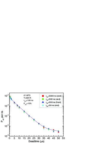
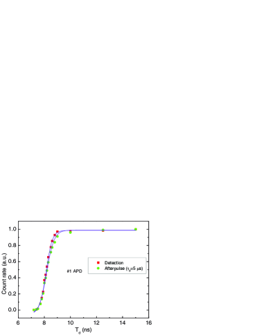
To illustrate the suitability for free-running operations we look at the as we make our detection gates longer. The results for #1 APD are plotted in Fig. 7 and fitted using the multiple trapping model. is fixed at ns while and the photon’s arrival positions are altered. If the active quenching was slow then the arrival position, or time, of the photon’s appearance in the gate would be reflected in the behavior. A photon creating an avalanche at the start of a long gate would generate more carriers, increasing the chances for subsequent afterpulses, than in the short gate regime or if the photon arrived at the end of a gate. The overlapping curves show that the behavior doesn’t change for long gates, nor is it dependent on the arrival time, and hence shouldn’t change when we move to a free-running regime.
| APD | T(K) | (ns) | (ns) | (ns) |
|---|---|---|---|---|
| #1 | 216 | 1135 | 5645 | |
| #1 | 238-223 | 860 | 4385 | |
| #2 | 210 | 615 | 2560 | 10135 |
| #2 | 238-223 | 1020 | 2165 | 5075 |
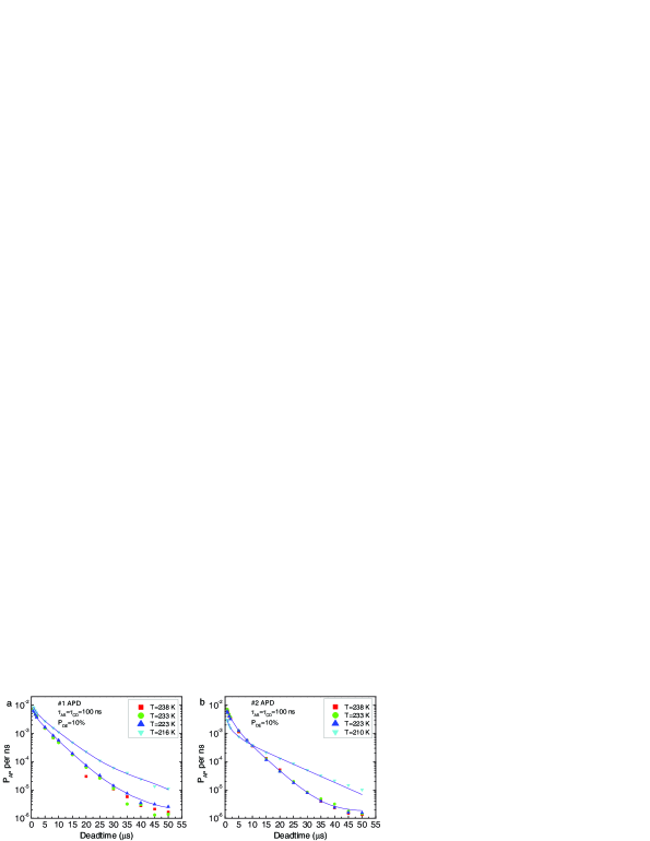
We finally study the temperature dependence of afterpulse. The experimental results and fitting curves are shown in Fig. 8 and the fitting parameters are listed in Table I. When the temperature is varied from K to K the behavior is almost identical due to the close trap lifetime parameters, but when the temperature is at K (#1 APD) or K (#2 APD), there is a distinct increase for the . The detrapping lifetime can be modeled as [27]
| (5) |
where is the trapping activation energy. This formula means that lower temperatures cause larger for traps, corresponding to larger .
Moreover, when s, the of #2 APD at K, in Fig. 8, is less than at other temperatures, but the of #1 APD at K is not. According to the fitting results at K, there is a trap type with a fast detrapping lifetime of ns in #2 APD, which causes rapid detrapping at small , but when becomes large, the effect of this trap type is gradually diminished while the other trap types with ns and ns lifetimes start to dominate the detrapping process. Unfortunately, this kind of fast detrapping time is too short and/or too weak to be measured at the other three temperatures and for #1 APD.
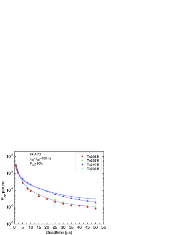
In order to validate the above phenomena, we perform the measurements of behaviors of #4 APD from another manufacturer, whose results are shown in Fig. 9. The increases from K to K while the cross point appears between K to K, which agrees well with our explanation for the different behaviors. We believe that the models so far are not perfect and further investigations, including effective models and experiments, are still needed.
III-D Free-running mode
Free-running operation is very important for many applications such as asynchronous and CW photon counting and quantum cryptography [1] etc. Due to the lower noise characteristics of InGaAs/InP APDs that use this active quenching ASIC, some of us have recently been able to show that this is now also possible for APDs in the telecom regime.
As in the gated regime, the operation in the free-running mode depends on the parameters of , and T. However, unlike the gated mode, the afterpulse parameter in the free-running mode is more difficult to evaluate.
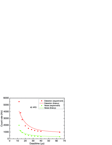
As we said, with respect to Fig. 7, the does not depend on the width of the gate, which is applicable for the free-running mode. Indeed, it may not be obvious how the afterpulse probablity evolves when the gate is open for such long times, though it would appear that at worst, the probability continues to decrease over the period of detection. Nonetheless, we have previously seen that for short deadtimes the afterpulsing dominates [24]. As we have now been able to use the double-gate method to characterize the afterpulsing, in the gated regime, we can use a simple model to describe the detection and noise rates for the free-running mode,
| (6) |
with , considering the Poisson distribution. and are the detection efficiency and dark count probability, and is the input photon number. The term of is for deadtime correction. If we put = 0, we recover the noise rate. is the total afterpulsing contribution at , calculated from integrating over the gated afterpulse probability from to infinity (in practice 100 s is sufficient). Fig. 10 shows the experimental rates as well as the results of our model as a function of .
It is clear that a more complicated model is warranted. However, the physics of these limitations is clear. In the small region we underestimate the rates as we do not take account of cascaded afterpulses, i.e., higher order effects. The more interesting region, from 20 - 40 s, we are overestimating due to the difficulty in defining an appropriate integration range, which will also change as a function of the photon flux, the intrinsic detection efficiency and the deadtime. Importantly, we can also conclude that for small , if increases, then the value will decrease, since photon clicks will increase while the multiple afterpulsing effects will be relatively less likely.
Our model makes a first attempt to both understand the afterpulsing and to develop a reliable technique for determining the detector’s characteristics, without resorting to complicated techniques in a double-gate regime, there is still some way to go. Although the apparent need for large that, in turn, limits the maximum count rate, this is highly dependent on the photon flux to be detected and free-running APDs are certainly highly advantageous for applications with low to moderate count rates.
III-E Charge persistence
Charge persistence is not normally a problem for synchronous detectors as the photons arrive during the gate. However, what happens if a photon arrives before the gate is applied, as is possible in the free-running mode, before the APD is activated after a deadtime?
When the detector is “off”, i.e., at below , with only a few volts so that primary dark carriers can still be generated and multiplied by the average dc gain but with a small probability. When the gate pulse arrives some of the carriers that remained in the multiplication layer can induce avalanches [28]. This is called “charge persistence” (CP), or sometimes referred as the “twilight effect” [29]. Similarly, when the CP carriers are released before the gate pulses with the time difference less than the effective transit time, they can also create afterpulses [28]. Now let us consider another case, where photons always appear before the gate. Based on the same principle, in this case the number of dark CP carriers will be increased and the CP effect will be expanded.
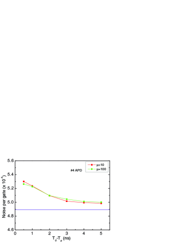
We experimentally test this effect and the results are shown in Fig. 11. By varying the time difference between the arrival times of gates (Td) and photons (Tp), we observe the changes of the normalized (for ) noise per gate, for #4 APD. The two almost identical behaviors show that the CP effect is proportional to photon numbers and, per photon, can generate noise of about of the dark count level with the time difference less than ns. When the time difference is larger than ns, the CP effect is negligible due to the characteristic exponential decrease. Moreover, through using TCSPC, we also observe the detection events at the beginning of the gate are more than those at other regions. The CP effect will cause nonnegligible noise in the case of high frequency gating or asynchronous high flux detection.
III-F Quenching time
Quantifying the quenching time, including the circuit reaction time and gate closing time as shown in Fig. 12, of an avalanche is very important to understand the avalanche dynamics of APDs. Although an active quenching ASIC should have a faster quenching time than conventional electronics this has not previously been measured. More generally, these results are also pertinent for rapid gating schemes that use very short gates and hence terminate avalanches very quickly.
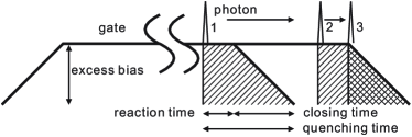
The principle for measuring the quenching time is to compare the count rate behaviors for detections and afterpulses, see Fig. 12, using the double-gate measurement electronics. The total number of carriers, during an avalanche, should be proportional to the excess bias on APD and the excess bias duration, or the integral of excess bias over the quenching time. Now we consider the case where photons arrive at the end of the detection gates, by delaying photons. From phase 1 to phase 2 in Fig. 12, the count rates of detection and afterpulse are both almost constant, while from phase 2 to phase 3 the detection rate is still constant but the afterpulse rate decreases first due to the decrease of the integral. The time difference between the two phases can be regarded as the reaction time, to detect the onset of the avalanche and send the signal to close the NMOS switch. After phase 3, both of the rates drastically decrease until the end of the closing time.
Fig. 13 shows the results of these measurements on #1 APD. From the slope of the detection rate, we can obtain the closing time of the gate, which is only around ns. Although it is very hard to determine a precise value of the reaction time from the fitting results, the slight shift between the detection and afterpulse rates indicates that the reaction time is much less than the closing time.
IV Conclusion
In summary, we have fully characterized an active quenching ASIC and compared its operation with a conventional electronic circuit. To show the improvements are universal we also characterized and compared 4 different InGaAs/InP APDs. The APDs operating in the gated mode exhibit substantial performance improvements compared with the conventional quenching electronics and allow for free-running operation. We also extract thermal activation energies to identify the dominant mechanism of dark counts, and by employing the multiple detrapping model in the gated mode and proposed model in the free-running mode the afterpulse behaviors are well illustrated. Moreover, we have characterized the charge persistence and quenching time. The advantages of low afterpulsing and noise in both theses regimes are mostly attributed to the state-of-the-art ASIC.
Acknowledgment
The authors would like to thank Dr. A. Rochas and Dr. M. A. Itzler for useful discussions.
References
- [1] N. Gisin, G. Ribordy, W. Tittel, and H. Zbinden, “Quantum cryptography,” Rev. Mod. Phys., vol. 74, pp. 145-195, Jan. 2002.
- [2] B. F. Levine, C. G. Bethea, and J. Campbell, “1.52 room temperature photon counting optical time domain reflectometer,” Electron. Lett., vol. 21, no. 5, pp. 194-196, Feb. 1985.
- [3] M. Wegmuller, F. Scholder, and N. Gisin, “Photon-Counting OTDR for local birefringence and fault analysis in the metro environment,” J. Lightwave Technol. vol. 22, no. 2, pp. 390-400, Feb. 2004.
- [4] F. Stellari, P. Song, J.C. Tsang, M.K. McManus, and M.B. Ketchen, “Testing and diagnostics of CMOS circuits using light emission from off-state leakage current,” IEEE Trans. on Electron Devices, vol. 51, no. 9, pp. 1455-1462, Sep. 2004.
- [5] Photomultiplier Tubes: Basics and Applications (3rd Edition). Hamamatsu Photonics, Hamamatsu City, Japan, 2006.
- [6] S. Cova, M. Ghioni, A. L. Lacaita, C. Samori, and F. Zappa, “Avalanche photodiodes and quenching circuits for single-photon detection,” Appl. Opt., vol. 35, no. 12, pp. 1956-1976, Apr. 1996.
- [7] J.C. Campbell, S. Demiguel, F. Ma, A. Beck, X. Guo, S. Wang, X. Zheng, X. Li, J.D. Beck, M.A. Kinch, A. Huntington, L.A. Coldren, J. Decobert, N. Tscherptner, “Recent advances in avalanche photodiodes,” IEEE J. Sel. Top. Quantum Electron., vol. 10, no. 4, pp. 777-787, Jul. 2004.
- [8] G. N. Gol’tsman, O. Okunev, G. Chulkova, A. Lipatov, A. Semenov, K. Smirnov, B. Voronov, A. Dzardanov, C. Williams, and R. Sobolewski, “Picosecond superconducting single-photon optical detector,” Appl. Phys. Lett., vol. 79, no.6, pp. 705-707, Aug. 2001.
- [9] S. Komiyama, O. Astafiev, V. Antonov, T. Kutsuwa, and H. Hirai, “A single-photon detector in the far-infrared range,” Nature (London), vol. 403, pp. 405-407, Jan. 2000.
- [10] A. Lacaita, F. Zappa, S. Cova, and P. Lovati, “Single-photon detection beyond : performance of commercially available InGaAs/InP detectors,” Appl. Opt., vol. 35, no. 16, pp. 2986-2996, Jun. 1996.
- [11] G. Ribordy, J.-D. Gautier, H. Zbinden, and N. Gisin, “Performance of InGaAs/InP avalanche photodiodes as gated-mode photon counters,” Appl. Opt., vol. 37, no. 12, pp. 2272-2277, Apr. 1998.
- [12] J. G. Rarity, T. E. Wall, K. D. Ridley, P. C. M. Owens, and P. R. Tapster, “Single-photon counting for the 1300-1600-nm range by use of Peltier-cooled and passively quenched InGaAs avalanche photodiodes,” Appl. Opt., vol. 39, no. 36, pp. 6746-6753, Dec. 2000.
- [13] P. A. Hiskett, G. S. Buller, A. Y. Loudon, J. M. Smith, I. Gontijo, A. C. Walker, P. D. Townsend, and M. J. Robertson, “Performance and Design of InGaAs /InP Photodiodes for Single-Photon Counting at ,” Appl. Opt., vol. 39, no. 36, pp. 6818-6829, Dec. 2000.
- [14] D. Stucki, G. Ribordy, A. Stefanov, H. Zbinden, J. G. Rarity, and T. Wall, “Photon counting for quantum key distribution with Peltier cooled InGaAs/InP APDs,” J. Mod. Opt., vol. 48, no. 13, pp. 1967-1981, Nov. 2001.
- [15] G. Karve, X. Zheng, X. Zhang, X. Li, N. Li, S. Wang, F. Ma, A. Holmes, J. C. Campbell, G. S. Kinsey, J. C. Boisvert, T. D. Isshiki, R. Sudharsanan, D. S. Bethune, and W. P. Risk, “Geiger mode operation of an avalanche photodiode,” IEEE J. Quantum Electron., vol. 39, no. 10, pp. 1281-1286, Oct. 2003.
- [16] G. Ribordy, N. Gisin, O. Guinnard, D. Stucki, M. Wegmuller, and H. Zbinden, “Photon counting at telecom wavelengths with commercial InGaAs/InP avalanche photodiodes: Current performance,” J. Mod. Opt., vol. 51, pp. 1381-1398, Jun. 2004.
- [17] D. A. Ramirez, M. M. Hayat, G. Karve, J. C. Campbell, S. N. Torres, B. E. A. Saleh, and M. C. Teich, “Detection efficiencies and generalized breakdown probabilities for nanosecnd-gated near infrared single-photon avalanche photodiodes,” IEEE J. Quantum Electron., vol. 42, no. 2, pp. 137-145, Feb. 2006.
- [18] S. Pellegrini, R. E.Warburton, L. J. J. Tan, J. S. Ng, A.B. Krysa, K. Groom, J. P. R. David, M. J. Robertson, and G. S. Buller, “Design and performance of an InGaAs-InP single-photon avalanche diode detector,” IEEE J. Quantum Electron., vol. 42, no. 4, pp. 397-403, Apr. 2006.
- [19] M. A. Itzler, R. Ben-Michael, C.-F. Hsu, K. Slomkowski, A. Tosi, S. Cova, F. Zappa, and R. Ispasoiu, “Single photon avalanche diodes (SPADs) for photon counting applications,” J. Mod. Opt., vol. 54, no. 2-3, pp. 283-304, Feb. 2007.
- [20] M. Liu, C. Hu, X. Bai, X. Guo, J. C. Campbell, Z. Pan, and M. M. Tashima, “High-performance InGaAs/InP single-Photon avalanche photodiode,” IEEE J. Sel. Top. Quantum Electron., vol. 13, no.4, pp. 887-894, Jul. 2007.
- [21] X. Jiang, M. A. Itzler, R. Ben-Michael, and K. Slomkowski, “InGaAsP-InP avalanche photodiodes for single photon detection,” IEEE J. Sel. Top. Quantum Electron., vol. 13, no. 4, pp. 895-905, Jul. 2007
- [22] X. Jiang, M. A. Itzler, R. Ben-Michael, and K. Slomkowski, M. A. Krainak, S. Wu, and X. Sun, “Afterpulsing Effects in Free-Running InGaAsP Single-Photon Avalanche Diodes,” IEEE J. Quantum Electron., vol. 44, no. 1, pp. 3-11, Jan. 2008
- [23] A. Rochas, C. Guillaume-Gentil, J-D. Gautier, A. Pauchard, G. Ribordy, H. Zbinden, Y. Leblebici, and L. Monat, “ASIC for high speed gating and free running operation of SPADs,” Proc. SPIE, vol. 6583, pp. 65830F-1-65830F-10, May. 2007.
- [24] R.T. Thew, D. Stucki, J.-D. Gautier, H. Zbinden, and A. Rochas, “Free-running InGaAs/InP avalanche photodiode with active quenching for single photon counting at telecom wavelengths,” Appl. Phys. Lett., vol. 91, no. 20, pp. 201114-1-201114-3, Nov. 2007.
- [25] J. P. Donnelly, E. K. Duerr, K. A. McIntosh, E. A. Dauler, D. C. Oakley, S. H. Groves, C. J. Vineis, L. J. Mahoney, K. M. Molvar, P. I. Hopman, K. E. Jensen, G. M. Smith, S. Verghese, and D. C. Shaver, “Design considerations for InGaAsP-InP Geiger-mode avalanche photodiodes,” IEEE J. Quantum Electron., vol. 42, no. 8, pp. 797-809, Aug. 2006.
- [26] M. A. Itzler, R. Ben-Michael, X. Jiang, and K. Slomkowski, “Geiger-Mode Avalanche Photodiodes for Near-Infrared Photon Counting,” in Conference on Lasers and Electro-Optics/Quantum Electronics and Laser Science Conference and Photonic Applications Systems Technologies, OSA Technical Digest Series (CD) (Optical Society of America, 2007), paper CMII1.
- [27] K. E. Jensen, P. I. Hopman, E. K. Duerr, E. A. Dauler, J. P. Donnelly, S. H. Groves, L. J. Mahoney, K. A. McIntosh, K. M. Molvar, A. Napoleone, D. C. Oakley, S. Verghese, C. J. Vineis, and R. D. Younger, “Afterpulsing in Geiger-mode avalanche photodiodes for wavelength,” Appl. Phys. Lett., vol. 88, no. 13, pp. 133503-1-133503-3, Mar. 2006.
- [28] Y. Kang, H. X. Lu, Y-H. Lo, D. S. Bethune, and W. P. Risk, “Dark count probability and quantum efficiency of avalanche photodiodes for single-photon detection,” Appl. Phys. Lett., vol. 83, no. 14, pp. 2955-2957, Oct. 2003.
- [29] S. V. Polyakov and A. L. Migdall, “High accuracy verification of a correlated-photon-based method for determining photoncounting detection efficiency,” Opt. Express, vol. 15, no. 4, pp. 1390-1407, Feb. 2007.