Co-induced nano-structures on Si(111) surfacenote
Abstract
The interaction of cobalt atoms with silicon (111) surface has been investigated by means of scanning tunneling microscopy (STM) and low-energy electron diffraction (LEED). Besides the Co silicide islands, we have successfully distinguished two inequivalent Co-induced reconstructions on Si (111) surface. Our high-resolution STM images provide some structural properties of the two different derived phases. Both of the two phases seem to form islands with single domain. The new findings will help us to understand the early stage of Co silicide formations.
I Introduction
Transition-metal silicides have been widely investigated in recent years in terms of microelectronic industry and fundamental science. Besides the applications of transition-metal silicides (such as CoSi2, NiSi2) in integrated-circuits, the effects of adsorbed atoms on a reconstructed Si surface and the mechanisms and coefficients of surface diffusion are also fundamental subjects of surface science. Although there have been extensive studies on the growth and properties of CoSi2 epitaxial films, knowledge about the structural details of Co adatoms and the initial stages of cobalt disilicide are insufficient partly due to an appearance of very rich reconstructed phases. Si(111)-R19.1∘-Co (hereafter as ) structure has been studied by means of LEED, XPS (X-ray Photoemission Spectroscopy), ARPES (Angle-Resolved Photoelectron Spectroscopy), STM and LDA (Local Density Approximation) based calculations Pirri29 ; Bennett69 ; Bennett48 . Two types of domains with R13.9∘ (hereafter as ) reconstructions and both the and R23.4∘ (hereafter as ) reconstructions were found by LEED and STM Dolbak373 ; Loffler81 , but the detailed structural information is still lacking. In order to investigate the detailed surface structures, STM experiment was carried out. In this paper, we will show two inequivalent Co-induced structural phases through several real space STM images together with their FFT (fast Fourier transformation) and LEED patterns.
II Experimental
The Co induced surface structures were fabricated and studied with a commercial room-temperature scanning tunneling microscope (STM, RHK UHV-400) mounted in an ultrahigh-vacuum (UHV) chamber combined with a sample-preparation chamber. The base pressures of the two chambers were around 1.010-10 Torr. Clean Si(111) (p type, 1000 cm) surfaces were obtained by the following process. After degassed for several hours at 800 K, the sample was flashed several times to 1470 K for 5 seconds, then the sample temperature was rapidly reduced to about 1170 K, and slowly decreased to room temperature at a pace of 12 K/s with a pressure below 1.010-9 Torr. The sample temperature was controlled by direct-current-heating and a nearly perfect 77 reconstruction was obtained by this method. Co was deposited from a water-cooled electron-beam evaporator (Omicron EFM 3) to clean 77-Si(111) surface with a rate of 0.08 ML/min (where 1 ML = 7.831014 atoms/cm2). The temperature of silicon substrate was kept at 800 K during the Co deposition. Auger electron spectroscopy (AES) and LEED observations were routinely carried out to check the surface cleanliness and reconstruction. All of the STM images were taken at room temperature.
III Results and discussion
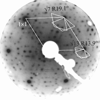
The LEED patten of 0.5 ML Co on Si(111) surface is presented in Fig. 1. Besides 11, 77 and patterns, one can find the spots of derived structure, which are the same as those in the published resultsDolbak373 . It should be mentioned here that these additional spots were formerly attributed to two types of domains with phase by Dolbak et al Dolbak373 , which were defined as A and B domains in their paper. The two kinds of domains are separated with respect to Si (10) mirror-image symmetry plane and they widely exist in structures such as Ni-induced twinned atomic structuresKinoda461 , Si(111)--Ag surface with different orientations of [11]10.89∘ at OPB3 (out-of-phase-boundary of the -Ag phase)Tong64 and so on. The present LEED pattern also indicates two domains for the surface phase as shown in Fig. 1.
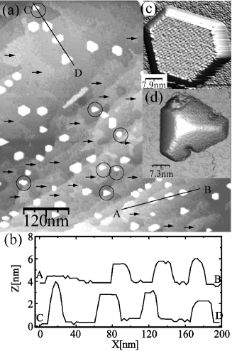
Fig. 2 (a) shows the typical occupied-state STM image in the wide area (600nm600nm, S = -2.5 V, S = 0.51 nA). Here, one can find some islands with larger height (brighter image). The cross sections along two lines marked on Fig. 2 (a) are shown in Fig. 2 (b). The lateral size of islands is in the order of tens nanometers, and mostly in the range between 20 to 50 nm with the height of about 25 nm. These islands can be classified into two typical types. The major one shows approximately triangular, trapezoidal or hexagonal shape with atomically flat top that shows well-known CoSi2(111)-(22) structure Bennett11 ; Zilani . A typical image of this kind of island is shown in Fig. 2 (c) in three dimensional form. The minority one as marked by ellipses in Fig. 2 (a) shows pyramid-like feature without any CoSi2(111)-(22) structure on the triangular flat top as seen in Fig. 2 (d). It is a little higher than the former type. The edges of both two types of islands are aligned parallel to those of the 77 unit cell, and the lengths are integer times as large as that of 77 unit cell as have been discussed elsewhereBennett11 . Due to the small percentage of island relative to the whole surface, the structures of the island surface did not reflect clear corresponding spots in LEED pattern. It means that the surface structures shown in LEED pattern mainly come from the contribution of inter island.
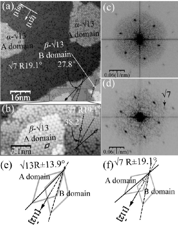
In the inter-island regions, besides 77, Co-induced and phases, one can find irregular flat areas with a height of about 0.3 nm (some typical regions were marked by black arrowheads in Fig. 2 (a)). More details of the occupied-state STM images in this region are shown in Figs. 3 (a) and (b). Here, two different structures are found. One shows a surface phase, which has been observed by Löffler et al Loffler81 (denoted as phase with A type domain). It is found that the length of unit cell is 1.38 nm and its orientation is rotated by an angle of 13.9∘ relative to [11] direction in clockwise direction as illustrated in Fig. 3 (e). Another structure in Fig. 3 (a) and magnified in Fig. 3 (b) has not been observed before. In order to know the structural property, we have analyzed the occupied-state STM image carefully. It is found that the unit cell size is around 1.38 nm and the unit cell is rotated by an angle of 13.9∘ in clockwise direction relative to [11] direction (illustrated in Fig. 3 (e)) indicating the same periodicity of in this new surface phase. To distinguish with - phase, this new phase is denoted as phase with A type domain. The fast Fourier transformation (FFT) images of Figs. 3 (a) and (b) using WSXM softwareHorcas78 are shown in Figs. 3 (c) and (d), respectively. The sharp FFT patterns of surface phases can be seen well note1 , and both of them show the same orientation, which together with their corresponding STM images gives the strong evidences of the two inequivalent surface phases.
It has been mentioned above that most surface phases on Si (111) surface have two domains with a misfit angle owing to Si (10) mirror-image symmetry planes shown in LEED pattern. For easily understood the different domains the schematic diagrams of the relationship of the different domains (here, A and B domains) for and reconstructions are shown in Figs. 3 (e) and (f). So, it is reasonable to observe both domains of the two phases on the surface (not shown here). It should be mentioned that both and phases seem to form islands with one domain, which is not like and structures that form twined structures with defects. The defect structures will restrain themselves from forming large islands. This feature indicates that the defect-free, single-domain island-like structures may be one kind of early-stage formation of Co silicide islands on Si (111) surface. From this point of view, the investigation of structures will help us to understand the early stage of Co silicide formations.
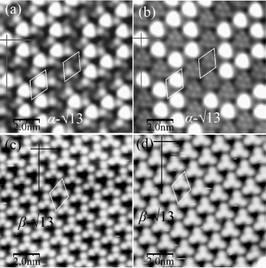
In order to study the detailed structures of surface phases, high-resolution STM observations have been performed. The empty- and occupied-state STM images of - (upper) and - (lower) phases are presented in Fig. 4 with the unit cell indicated in the figures. The prominent feature of both surface phases is the centered hexagonal array of threefold symmetric protrusions as is evident in Fig. 4. Note that the phase seems to comprise two layers of triangular clusters on the top and another triangle with six protrusions below them as shown in the occupied-state STM image (Fig. 4 (b)). Both of them just occupies half of the unit cell (here after as HUC), the other half is a dark hole at negative sample bias( shown in Fig. 4 (b)). For the lower layer, at a negative sample bias, the triangle with six protrusions and the other dark HUC can be observed, while at positive sample bias the dark HUC becomes brighter and the number of protrusions is reduced to three at the corner with a dark hole in the center. For the upper layer, it is noticed that the bright triangle always occupies the same HUC – on the top of six-protrusion triangle in occupied-states – and the positions of the bright triangle are not changed at various sample bias, which means that the protrusions of the bright triangle give the sites information of real atoms.
The expanded high-resolution phase images show four protrusions (tetramers) and a dark HUC in both empty- and occupied-states. In contrast to the phase, the phase exhibits a little difference in spatial distribution between empty- and occupied-state, except the protrusions in occupied-state STM images seem fatter than that in empty-state STM images. It should be mentioned that we still can not give the information of Co atoms contribution in - and - surface phases just from STM image. For more information, deeper investigation and a atomic structural model need to be made and some calculated results should be helpful.
IV Conclusion
In summary, self-assembled Co silicide have been fabricated on Si(111) and investigated by means of scanning tunneling microscopy (STM) and low-energy diffraction (LEED). The LEED pattern has verified the existence of phases on Si(111) surface. Our high resolution STM images show that besides the Co silicide island, there are two inequivalent surface phases in the inter-island regions. Both of the two phases seem to form islands with single domain. From this point of view, the new findings will help us to understand the early stage of Co silicide formations.
This work was supported by the Ministry of Education, Culture, Sports, Sciences and Technology of Japan.
References
- (1) Published in Applied surface science 254 (2008) 7684-7687 doi:10.1016/j.apsusc.2008.01.136
- (2) C. Pirri, J. C. Peruchetti, G. Gewinner and J. Derrien, Phys. Rev. B 29 (1984) 3391; B 30 (1984) 6227.
- (3) P. A. Bennett, M. Copel, D. Cahill, J. Falta and R. M. Tromp, Phys. Rev. lett. 69 (1992) 1224.
- (4) M. -H. Tsai, J. D. Dow, P. A. Bennett, D. G. Cahill, Phys. Rev. B 48 (1993) 2486.
- (5) A. E. Dolbak, B. Z. Olshanetsky, S. A. Teys, Surf. Sci. 373 (1997) 43.
- (6) M. Löffler, J. Cordón, M. Weinelt, J. E. Ortega, T. Fauster, Appl. Phys. A 81 (2005) 1651.
- (7) G. Kinoda, K. Ogawa, Surf. Sci. 461 (2000) 67.
- (8) Xiao Tong, Satoru Ohuchi, Norio Sato, Takehiro Tanikawa, Tadaaki Nagao, Iwao Matsuda, Yoshinobu Aoyagi, and Shuji Hasegawa, Phys. Rev. B 64 (2001) 205316
- (9) P. A. Bennett, S. A. Parikh, D. G. Cahill, J. Vac. Sci. Technol. A 11 (1993) 1680.
- (10) M. A. K. Zilani, Lei Liu, H. Xu, Y. P. Feng, X. -S. Wang and A. T. S. Wee, J. Phys.: Condens. Matter 18 (2006) 6987
- (11) I. Horcas, R. Fermández, J. M. Gómez-Rodríguez, J. Colchero, J. Gómez-Herrero, A. M. Baro, Rev. Sci. Instrum. 78 (2007) 013705.
- (12) One can see a large number of reconstructions from the STM images (See Figs. 3 (a) and (b)). Since there are many defects in phases, one can not get very sharp FFT spots with structure. The irregular lattices just contribute to a dark background as shown in Figs. 3 (c) and (d).