A Rad-hard CMOS Active Pixel Sensor
for Electron Microscopy
Abstract
Monolithic CMOS pixel sensors offer unprecedented opportunities for fast nano-imaging through direct electron detection in transmission electron microscopy. We present the design and a full characterisation of a CMOS pixel test structure able to withstand doses in excess of 1 MRad. Data collected with electron beams at various energies of interest in electron microscopy are compared to predictions of simulation and to 1.5 GeV electron data to disentagle the effect of multiple scattering. The point spread function measured with 300 keV electrons is (8.1 1.6) m for 10 m pixel and (10.9 2.3) m for 20 m pixels, respectively, which agrees well with the values of 8.4 m and 10.5 m predicted by our simulation.
keywords:
Monolithic active pixel sensor, Transmission Electron Microscopy;, , , , , , , ,
1 Introduction
CMOS monolithic active pixel sensors were first proposed as photo-detectors forty years ago. About a decade ago their use as charged particle detectors started to be explored, recognising that they represent an appealing technology offering small pixel size and the possibility of high speed read-out [1, 2]. In addition to their use in charged particle tracking, they have been proposed and investigated for direct electron detection in electron microscopy, in particular in Transmission Electron Microscopy (TEM) as electron imagers [3, 4, 5] together with hybrid pixels [6, 7, 8], as an advantageous alternative to CCDs optically coupled to phosphor plates (for a review of different detection technologies, see [9]).
For single particle tracking, it has been demonstrated that CMOS pixels of order 1010 m2 can reconstruct the position of impact of the particle with an accuracy of , by using the centre of gravity of the charge distribution [10]. Owing to their thin sensitive region, confined to the 10 m lightly-doped epitaxial layer, these sensors can be back-thinned down to 50 m, without loss in performance [11]. The thin charge-collection region and total thickness of CMOS pixel sensors is ideal in TEM applications, where multiple scattering effects are significant, for obtaining a good Point Spread Function (PSF). In the energy region of interest in TEM, which is 60 - 400 keV, the specific energy loss, , varies by an order of magnitude but remains large enough to ensure single electron detection with large signal-to-noise ratio (S/N) values. For TEM, the detector should record the position of a collection of electrons that represents a magnified image. Whereas diffusion is beneficial for tracking applications, as it improves the determination of the charge centre of gravity, and thus of the particle impact point, to an accuracy significantly better than the pixel pitch, for TEM diffusion is harmful, as it increases the PSF and needs to be carefully evaluated.
While significant progress has been made in the last few years to develop CMOS pixel sensors for tracking and vertexing applications in particle collider experiments, several issues, relevant to their application for fast nano-imaging at TEM, remain to be addressed. In particular, their radiation hardness is a key challenge in the design of a detector for TEM. Unlike HEP, where the total dose requirement can be estimated, based on integrated luminosity, TEM requirements depend on the mode of operation. Whereas the radiation hardness for the specimen can be easily specified (in electrons per square angstrom), as the magnification is variable, this does not translate into a requirement on the detector. In addition, large numbers of electrons may be contained in a limited number of Bragg spots, when operating in diffraction mode, causing large doses to be received by a small number of pixels. Given that a very intense bright field image could deposit order of 10 rad s-1 pixel-1, a target radiation tolerance of 1 MRad would enable its use for approximately one year, which appears to be a valid requirement.
In this paper we present a prototype CMOS active pixel sensor with radiation tolerant pixel cell design for use in TEM. We evaluate its performance applying high energy physics (HEP) modelling and experimental techniques to their characterisation as TEM detectors. We study the particle energy loss, charge spread, point spread function and response after irradiation with 200 keV electrons and 29 MeV protons for doses in excess to 1 MRad. Data are compared to results of detailed simulation of electron interactions, energy loss and signal generation.
2 Sensor Design and Readout
We developed a new circuit, named LDRD2-RH, optimised for radiation tolerance, as a variation on a previous circuit, developed for HEP applications [12]. The LDRD2-RH chip retains the original addressing and output circuitry. The sensor is divided into several sectors, each consisting of 2448 pixels arrayed on a 20 m pitch, in order to test different pixel layouts. The principle radiation damage mechanism is radiation-induced leakage current in the charge-collecting diode. This leakage current is primarily caused by the positive potential generated by trapped (positive) charge in the oxide above the p-type silicon, which results in inversion of the silicon at the Si/SiO2 interface. In each 2020 m2 pixel, two 1020 m2 pixels are drawn: each with the same design of the charge-collecting diode, and with the classical 3T-readout. For both sub-pixels, the transistor sizes (W/L) are the same, but in one sub-pixel the transistor has a conventional linear layout, and in the other, an enclosed gate layout. Figure 1 shows some of the different diode layouts used.

The detector has been fabricated in the AMS 0.35 m 4-metal, 2-poly CMOS-OPTO process, which has an epitaxial layer with a nominal thickness of 14 m.
Pixels are read out in rolling shutter mode, which ensures a constant integration time across the pixel matrix. Pixels are clocked at 6.25 MHz and 25 MHz, corresponding to an integration time of 737 s and 184 s, respectively. The detector is readout through a custom FPGA-driven acquisition board. A set of 14 bits, 40 MSample/s ADCs reads the chip outputs, while an array of digital buffers drives all the required clocks and synchronisation signals. The FPGA has been programmed to generate the clock pattern and collect the data sampled by the ADCs. A 32 bit-wide bus connects the FPGA to a National Instruments PCI 6533 digital acquisition board installed on the PCI bus of a control PC. Data is processed on-line by a LabView-based program, which performs the computation of the pixel noise and pedestal levels. Results are given for the PO pixel design, which was found to be best performing in terms of radiation tolerance, read out at 6.25 MHz, unless otherwise noted.
3 Response Simulation
The energy deposition in the sensor active layer and the lateral charge spread is simulated using two independent programs.
The simulation of electron scattering in matter for applications in electron microscopy has been described in [13]. The first simulation program is inspired by this formalism, but with the relativistic corrections added, as required for accuracy at our energies of interest. The second simulation is based on the Geant-4 program [14] and uses the low energy electromagnetic physics models [15].
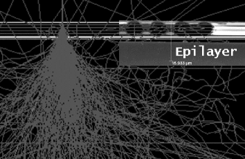
In both simulations, the CMOS sensor is modelled according to the detailed geometric structure of oxide, metal interconnect and silicon layers, as specified by the foundry. Electrons are incident perpendicular to the detector plane and tracked through the sensor. For each interaction within the epitaxial layer, the energy released and the position are recorded. Figure 2 shows the sensor layout adopted in the simulation with the simulated trajectories of 200 keV electrons.
 |
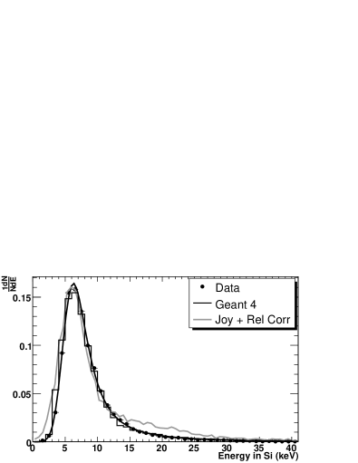 |
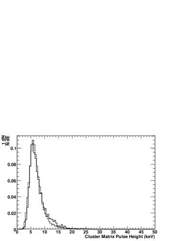
The two simulation programs give a good description of the measured energy deposition as shown in Figure 2. Geant-4 provides with a better description of the high energy part of the Landau distribution which tends to be systematically over-estimated by the results of the first simulation program. This effect becomes more significant with increasing electron energies.
The lateral charge spread due to multiple scattering in the sensor is evaluated in simulation by computing the lateral position of the electron interaction points in the epitaxial layer, weighted by the deposited energy. Results from the Geant-4 simulation are given in Table 1.
| Lateral Spread | |
|---|---|
| (m) | |
| 120 keV | 15.6 |
| 160 keV | 11.5 |
| 200 keV | 9.3 |
| 300 keV | 6.8 |
| 1.5 GeV | 1.3 |
Charge collection is simulated with PixelSim, a dedicated digitisation module [16], developed in the Marlin C++ reconstruction framework [17]. This processor starts from the ionisation points generated along the particle trajectory by Geant-4 and models the diffusion of charge carriers from the epitaxial layer to the collection diode. PixelSim provides us with full simulation of the response of all the individual pixels in the detector matrix, including electronics noise and efficiency effects, which can be processed through the same analysis chain as the data. The simulation has a free parameter, the diffusion parameter , used to determine the width of the charge carrier cloud, which is tuned to reproduce the pixel multiplicity in the cluster measured for 1.5 GeV electrons in data, as discussed in the next section. We find the best agreement between the simulated and measured pixel multiplicity in the cluster for = 16.5 m. This can be compared with an estimate of the charge diffusion length , obtained from the diffusion coefficient, , and the charge collection time, . The diffusion coefficient is computed for an estimated doping of - cm-3 of the epitaxial layer. The charge collection time has been measured on data. We focus a 1060 nm laser to a 10 m spot onto a single pixel and pulse the laser for 2 ns. The pixel analog output is recorded on a digital oscilloscope and we observe that the pixel analog level reaches a plateau 150 ns after the arrival of the laser pulse. From these data we estimate a diffusion length of 14 m - 19 m, which agrees well with the simulation result.
4 Sensor Tests
4.1 Energy Deposition
The detector calibration is obtained by recording the position of the 5.9 keV full energy peak of a collimated 2.2 mCi 55Fe source. We find a conversion factor of 0.98 keV/ADC count or 26.7 /ADC count at 6.25 MHz readout frequency.
Electrons in the energy range from 120 keV to 200 keV from the 200CX electron microscope at the National Center for Electron Microscopy (NCEM) are used to characterise the detector response to low energy particles. The response to high momentum particles is studied with the 1.5 GeV electron beam extracted from the LBNL Advanced Light Source (ALS) booster. Data are converted into the lcio format [18]. Data analysis is performed offline by a set of dedicated processors developed in Marlin and proceeds as follows. Events are first scanned for noisy pixels. The noise and pedestal values computed on-line are updated, using the algorithm in [19], to follow possible variations in the course of data taking. The measured average pixel noise is (130 6) and (71 4) of equivalent noise charge (ENC) for the electron microscope and the ALS data respectively at 6.25 MHz and (110 8) and (67 5) at 25 MHz. The noise is partly due to the readout electronics, and is larger in the electron microscope setup due to the longer cable needed to route the analog signals out of the vacuum enclosure at the bottom of the microscope column, with a minor contribution from leakage current from operating the detector at +25∘C.
Electron hits are then reconstructed from the recorded pixel pulse heights. The detector is scanned for pixels with pulse height values over a given S/N threshold. These are designated as cluster ‘seeds’. Seeds are sorted according to their pulse heights and the surrounding neighbouring pixels are tested for addition to the cluster. The neighbour search is performed in a 55 matrix around the seed. Pixel thresholds at 3.5 and 2.0 units of noise have been used for seed and additional pixels, respectively. Clusters are not allowed to overlap, i.e. pixels already associated with one cluster are not considered for populating another cluster around a different seed. Finally, we require that clusters are not discontinuous, i.e. pixels associated to a cluster cannot be interleaved by any pixel below the neighbour threshold. Reconstructed hits are characterised in terms of the energy recorded in a 33 pixel matrix centred around the seed pixel, the pixel multiplicity of the reconstructed cluster and the fraction of the total charge collected by the pixels in the matrix, sorted in order of decreasing pulse height.
 |
 |
 |
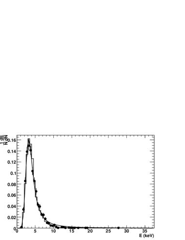 |
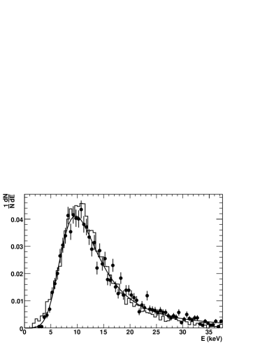
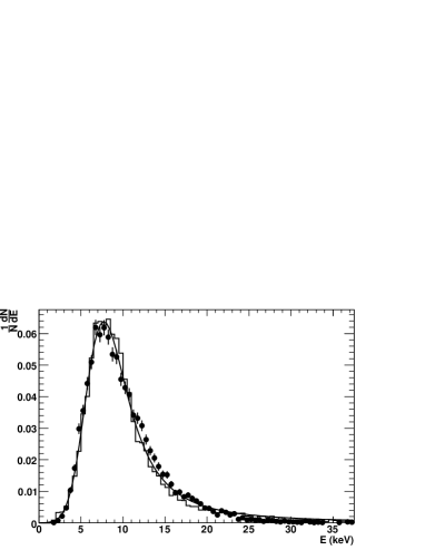
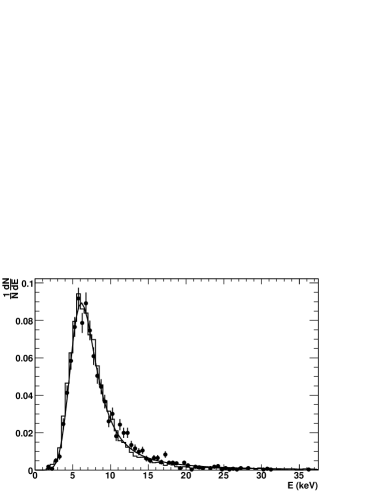
Results for the reconstructed deposited energy are shown in Figure 3, where data and simulation for 120 keV, 160 keV, 200 keV and 1.5 GeV electrons are compared. The simulation reproduces well the measured energy deposition, over this range of particle energies. The observed average values of energy deposition exceeds those predicted by the thin straggling model [20] for 14 m of Si, due to the effect of electron interactions in the SiO2 and metal layers on top of the sensitive volume.
4.2 Charge Spread
The lateral charge spread is studied from the shape of the reconstructed clusters. The two variables used are the cluster size, i.e. the average pixel multiplicity , and the distribution of the fraction of the total charge collected in the pixels with the highest pulse height in a matrix around the seed pixel. Table 2 compares the cluster size for electrons of different energies measured in data with the simulation prediction.
| (keV) | Data | Simulation |
|---|---|---|
| 120 keV | 3.35 0.06 | 3.01 0.02 |
| 160 keV | 2.82 0.04 | 2.73 0.03 |
| 200 keV | 2.25 0.04 | 2.33 0.03 |
| 1.5 GeV | 2.20 0.02 | 2.21 0.02 |
The cluster size for 1.5 GeV electrons is governed by the charge carrier diffusion in the epitaxial layer, since the multiple scattering is negligible compared to the pixel size, at this energy. Both data and simulation show an increase of the multiplicity for lower energies consistent with the combined effect of the larger collected charge, which pushes the pulse height on more pixels above the S/N threshold for additional pixels, and of the multiple scattering in the detector, which displaces the locations of energy deposition from the point of entrance of the electron.
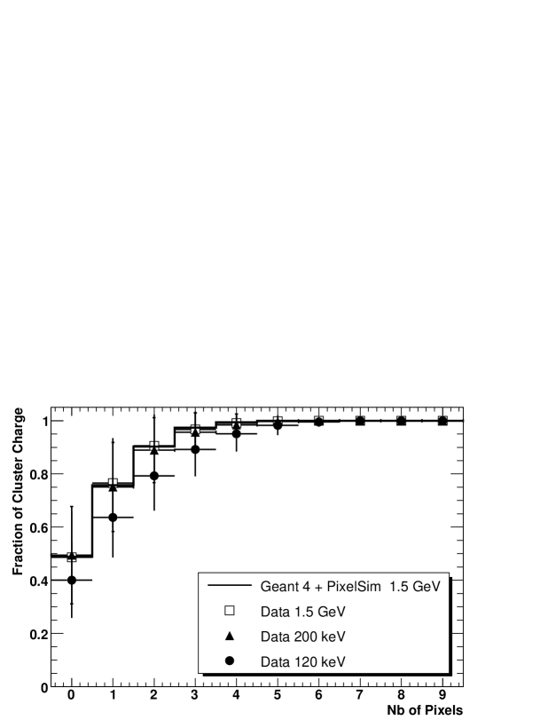 |
The two effects can be disentangled by analysing the fraction of the cluster charge collected in the pixels with the highest pulse height in a 33 matrix around the cluster seed. Figure 4 shows the results obtained for data at 120 keV and 200 keV compared to 1.5 GeV electrons. We indeed observe an increase of the area over which the charge spreads with 120 keV electrons, consistent with the effect of lateral charge spread due to multiple scattering which becomes of the order of the pixel size. On the contrary there is no significant increase on the charge distribution for 200 keV electrons, where we also observe only a very modest increase in cluster size. These results are well reproduced by simulation as shown in Figure 4. This first validation of simulation in the description of charge spread is important for its use in the PSF estimation, which is discussed next.
4.3 Point Spread Function and Imaging
The detector point spread function originates from charge spread due to charge carrier diffusion and ionising particle scattering, as well as by the finite spatial sampling frequency, which depends on the pixel pitch. We estimate the point spread function using Geant-4 + PixelSim simulation and test the simulation results with data. In simulation, a monochromatic, point-like beam of electrons is sent onto the surface of the detector. The point spread function is determined as the r.m.s. of the predicted distribution of the detected charge on the pixels. Results are summarised in Table 3 for different electron energies and 10 m and 20 m pixel pitch. Simulation predicts a PSF better than 10 m for 300 keV electrons imaged with a 10 m pixel pitch.
| Energy | 10 m | 20 m |
|---|---|---|
| (keV) | Pixels | Pixels |
| 120 | 11.4 | 13.1 |
| 200 | 9.1 | 11.2 |
| 300 | 8.4 | 10.5 |
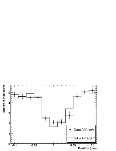
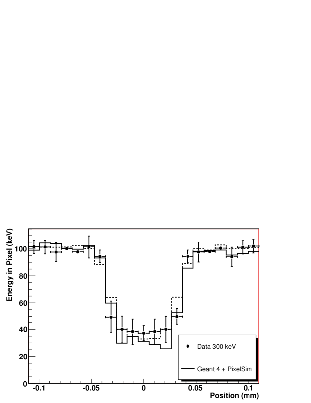
We validate these results using data taken at different energies, from 100 keV up to 300 keV, with 10 m and 20 m pixels at the TITAN test column at NCEM. We use the LDRD2-RH as well as an earlier sensor, the LDRD1 chip, featuring simple 3T pixels with 10 m, 20 m and 40 m pitch and fabricated in the same AMS 0.35-OPTO process [21]. A gold wire was mounted, parallel to the pixel columns, at a distance of 3 mm from the detector surface. The wire diameter is measured to be (59.60.7) m, using a high resolution optical survey system. Since the gold wire has well-defined edges, the profile of the deposited energy in the pixels, measured across the wire allows us to study the charge spread due to scattering and diffusion along the projected image of the wire edge and compare to simulation.
 |
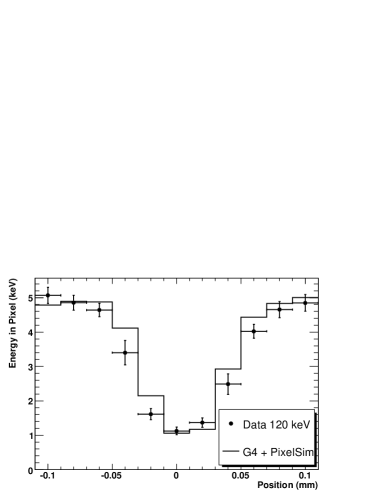 |
The setup has been simulated in detail in Geant-4 and the pixel response extracted from PixelSim. We study the change in the recorded signal, by scanning along pixel rows across the gold wire. Figure 5 shows the pulse heights measured on the pixels along a set of rows, comparing data at 300 keV and 120 keV with simulation, for the 20 m pixel pitch. The good agreement observed validates the estimation of the point spread function obtained from simulation.
 |
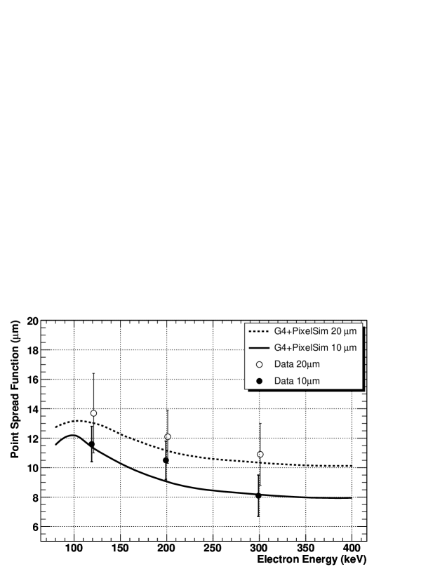 |
Further, we extract the point spread function directly from the data and compare the results to the simulation predictions. We parametrise the measured pulse height on pixel rows across the image projected by the wire with a box function smeared by a Gaussian term, which describes the point spread function. The maximum and minimum pulse height levels, for pixels away from the wire region and for the pixel exactly below the wire centre, respectively, are fixed to those observed in data and we perform a simple 1-parameter fit to extract the Gaussian width term, which gives the PSF. At 300 keV, we measure a PSF value of (8.1 1.6) m for 10 m pixels on the LDRD1 chip (see Figure 6) and of (10.9 2.3) m for 20 m pixels on the LDRD2-RH chip, to be compared to simulation which predicts 8.4 m and 10.5 m, respectively. The PSF scaling with electron energy and pixel size is shown in Figure 6. Again data and simulation are in good agreement. It is interesting to observe that for increasing electron energies the point spread function improves, due to the reduction of multiple scattering, up to 300 keV, where it approaches an asymptotic value for 10 m pixels, dominated by the effect of charge spread and spatial sampling frequency. On the opposite end of the energy range, the point spread function grows to a maximum around 100 keV and simulation predicts it to fall for lower energies, due to the short range in Si of these soft electrons.
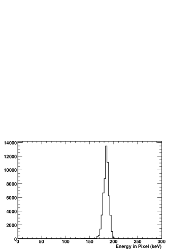
Finally, we have performed a realistic imaging test with the LDRD2-RH sensor, by acquiring images of nanoparticles of a 91.8 % Pb + 8.2 % Sn alloy embedded in a solid Al matrix [22] at the 200CX electron microscope. The images are obtained with a 200 keV electron flat field illumination at 6.25 MHz readout frequency and 50 frames s-1 are written to disk. We estimate the flux to be 35 pixel-1 event-1, where one event corresponds to a 737 s integration time.
 |
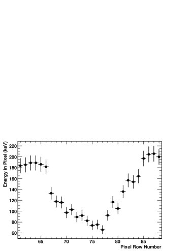 |
Figure 7 shows the pulse height recorded on the pixels across the projected image of a nanoparticle.
5 Sensor Irradiation
The radiation tolerance of the LDRD2-RH chip for use in TEM has been assessed by comparing the sensor response before and after irradiation with 200 keV electrons up to a dose in excess of 1 MRad. Results have been integrated by an irradiation with 29 MeV protons at the LBNL 88-inch cyclotron. We study the pixel noise, leakage current and charge collection. All tests are performed at room temperature.
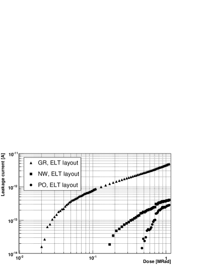
For the electron irradiation, the sensor active surface has been covered with a same gold mesh, having 50 m wide bars and 204 m wide holes. This allows to compare the response of irradiated and non-irradiated pixels on the same chip. The sensor has been irradiated with a flux of 2300 s-1 m-2, in multiple steps, up to a total estimated dose of 1.11 MRad. In between consecutive irradiation steps, 100 events are acquired without beam and the pixel pedestals and noise computed, in order to monitor the evolution of the pixel leakage current with dose. Figure 8 shows the increase of the pixel pedestal levels, which measure the leakage current, as a function of the integrated dose.
 |
 |
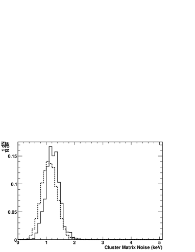
After irradiation the sensor response is tested with 200 keV and 1.5 GeV electrons. The deposited energy in the 33 pixel matrix is compared to that obtained before irradiation. We fit the energy spectrum with a Landau function convoluted with a Gaussian distribution to represent the noise contribution. The fit function has three free parameters, the Landau peak position (Landau m.p.v.), the Gaussian width (Gaussian Noise) and an overall normalisation. Due to the large correlation between the Gaussian width and the Landau width, the latter is fixed in the fit to the value obtained on simulation. We observe a change of the gain by 1.35, confirmed by calibration with 55Fe. After correcting for this gain shift, the noise and energy deposition distributions before and after irradiation are in good agreement. In the ALS data, taken with shorter connections between the detector and the digitiser board, the electronics noise is lower and an hint of a small increase of the detector noise after irradiation may be observed. The deposited energy spectrum is unchanged after irradiation, confirming that the charge collection properties of the pixel cell are not affected. Results are summarised in Figure 9 and Table 4.
 |
 |
| Before | After | |
| Irradiation | Irradiation | |
| 200 keV | ||
| Landau m.p.v. | (5.570.04) keV | (5.540.04) keV |
| Gaussian Noise | (1.190.04) keV | (0.980.03) keV |
| 33 Matrix Noise | (1.220.20) keV | (1.110.20) keV |
| 1.5 GeV | ||
| Landau m.p.v. | (3.050.03) keV | (3.370.07) keV |
| Gaussian Noise | (0.600.06) keV | (0.810.07) keV |
| 33 Matrix Noise | (0.740.01) keV | (0.880.01) keV |
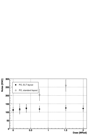
Since the threshold energy for electrons to cause displacement damage in silicon is 260 keV [23], we expect 200 keV to create only ionising damage. We investigated the effect of 29 MeV protons, which damage the sensor via both ionisation and non-ionising energy loss. The irradiation has been performed at the BASE Facility of the LBNL 88-inch cyclotron [24]. Results are reported in details in [25]. One prototype sensor was irradiated with 29 MeV protons up to a total integrated fluence of 8.51012 p/cm2, corresponding to a total dose of 2 MRad. At equal doses, a larger increase of the leakage current, compared to the electron irradiation, hints at a probable contribution from displacement damage. Figure 8 (right) shows the average pixel noise in the PO sectors for ELT and linear transistors; it can be seen that while the noise of the ELT layout cells remains basically unchanged over the dose range and only slightly increases at the highest doses, the noise of the standard layout cells is doubled after 1 MRad. The increased leakage current can be controlled by cooling the chip. The PO design with ELT layout appears to be the most radiation tolerant of the designs tested in the LDRD2-RH chip.
6 Conclusions
Thin monolithic CMOS pixel sensors with small, radiation tolerant pixels offer a very attractive solution for fast nano-imaging in transmission electron microscopy. The thin sensitive layer ensures a direct detection with small multiple scattering contribution to the point spread function. Fast readout and single electron sensitivity in small pixel cells result in high resolution dynamic imaging. We have developed a prototype CMOS pixel sensor implementing radiation tolerant cells. The sensor response in terms of energy deposition, charge spread and point spread function has been extensively tested for electrons in the energy range of interest for TEM. A detailed simulation based on Geant-4 and a dedicated charge generation and collection simulation package has been validated on the data recorded.
The point spread function measured with 300 keV electrons is (8.1 1.6) m for 10 m pixel and (10.9 2.3) m for 20 m pixels, respectively, which agrees well with the values of 8.4 m and 10.5 m predicted by our simulation.
The radiation tolerance of pixels with enclosed transistors and specific diode design has been verified with 200 keV electrons and 29 MeV protons. The pixel cells withstand doses in excess to 1 MRad, without significant degradation in noise and charge collection efficiency, making them well suited for a sensor for direct detection in TEM.
Acknowledgements
We wish to thank Thomas Duden, Rolf Erni, Michael Johnson, Zhongoon Lee, Peggy McMahan, Marta Rossell Abrodos and the staff of the ALS and the 88-inch cyclotron for assistance and for the excellent performance of the accelerators. This work was supported by the Director, Office of Science, of the U.S. Department of Energy under Contract No.DE-AC02-05CH11231.
References
- [1] E.R. Fossum, IEEE Trans. Electron. Devices 44 (1997) 1689.
- [2] R. Turchetta et al., Nucl. Instrum. and Meth. A 458 (2001) 677.
- [3] A.-C. Milazzo et al, Ultramicroscopy 104 (2005) 152.
- [4] G. Deptuch et al., Ultramicroscopy 107 (2007) 674.
- [5] P. Denes, J.-M. Bussat, Z. Lee, V. Radmillovic, Nucl. Instrum. Meth. A 579 (2007) 891.
- [6] G.Y. Fan et al., Ultramicroscopy 70 (1998) 113.
- [7] A.R. Faruqi, D.M. Cattermole, C. Reburn, Nucl. Instrum. Meth. A 513 (2003) 317.
- [8] A.R.Faruqi et al., Ultramicroscopy 94 (2003) 263.
- [9] A.R. Faruqi and R. Henderson, Current Opinion in Structural Biology 17 (2007) 549.
- [10] Yu. Gornushkin et al., Nucl. Instrum. and Meth. A 513 (2003) 291.
- [11] M. Battaglia, D. Contarato, P. Giubilato, L. Greiner, L. Glesener and B. Hooberman, Nucl. Instrum. Meth. A 579 (2007) 675.
- [12] M. Battaglia et al., to appear on IEEE, Trans. Nucl. Sci. 55 (2008).
- [13] D. Joy, Monte Carlo Modeling for Electron Microscopy and Microanalysis, Oxford University Press, New York, 2005.
- [14] S. Agostinelli et al., Nucl. Instrum. Meth. A 506 (2003) 250.
- [15] S. Chauvie, G. Depaola, V. Ivanchenko, F. Longo, P. Nieminen and M. G. Pia, Prepared for CHEP’01: Computing in High-Energy Physics and Nuclear, Beijing, China, 3-7 September 2001
- [16] M. Battaglia, Nucl. Instrum. Meth. A 572 (2007) 274.
- [17] F. Gaede, Nucl. Instrum. Meth. A 559 (2006) 177.
- [18] F. Gaede, T. Behnke, N. Graf and T. Johnson, in the Proc. of 2003 Conf. for Computing in High-Energy and Nuclear Physics (CHEP 03), La Jolla, California, 24-28 March 2003, pp TUKT001, [arXiv:physics/0306114].
- [19] V. Chabaud et al., Nucl. Instrum. Meth. A 292 (1990), 75.
- [20] H. Bichsel, Nucl. Instrum. Meth. B 52 (1990), 136.
- [21] M. Battaglia et al., in the Proc. of the International Symposium on Detector Development for Particle, Astroparticle and Synchrotron Radiation Experiments (SNIC 2006), Menlo Park, California, 3-6 April 2006, ECONF-C0604032, pp 0108.
- [22] H. Gabrisch, L. Kjeldgaard, E. Johnson, U. Dahmen, Acta Materialia 49 (2001), 4259.
- [23] G. Lindström, Nucl. Instrum. Meth. A 512 (2003), 30.
- [24] M.A. McMahan, Nucl. Instrum. Meth. B 241 (2005), 409.
- [25] M. Battaglia et al., to be submitted to IEEE, Trans. Nucl. Sci. (2008).