On the Origin of the 2DEG Carrier Density at the LaAlO3/SrTiO3 Interface
Abstract
Transport measurements of the two-dimensional electron gas (2DEG) at the LaAlO3/SrTiO3 interface have found a density of carriers much lower than expected from the “polar catastrophe” arguments. From a detail density-functional study, we suggest how this discrepancy may be reconciled. We find that electrons occupy multiple subbands at the interface leading to a rich array of transport properties. Some electrons are confined to a single interfacial layer and susceptible to localization, while others with small masses and extended over several layers are expected to contribute to transport.
pacs:
73.20.-r,73.21.-bIn a seminal paper, Ohtomo and Hwangohtomo reported the observation of a conducting layer of electrons at the interface between two insulators LaAlO3 (LAO) and SrTiO3 (STO). The carrier density was quite high, of the order of cm-2, as also the mobility, leading to the prospect for high-performance oxide electronics. Consequently, considerable attention has been focused on the understanding of the origin of these charge carriers.eckstein Systematic experiments on oxygen annealed samples as well as on samples grown under high oxygen pressure conditions have tuned down the carrier density to about cm-2, which is now the common carrier density observed by several groups.brinkman ; kalabukov ; beasley ; fert ; thiel Thus the emerging consensus is that the higher carrier density cm-2, originally observed, is due to the electrons released by the oxygen vacancies and they have a 3D character, while the lower carrier density cm-2 may be an intrinsic feature of the interface. However, this intrinsic carrier density is much smaller than the 0.5 electrons per unit cell ( cm-2) needed to suppress the “polar catastrophe,”harrison-cat which arises because of the diverging Coulomb field due to the polarity of the individual layers (Fig. 1). Thus the origin of the carrier density for the intrinsic interface is poorly understood and remains a key puzzle for these interfaces.
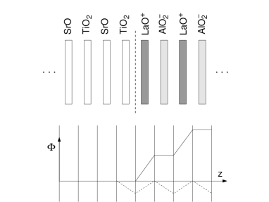
In this paper, we suggest a solution for this puzzle based on the results of our detail density-functional study of the electronic structure. Although there also exists a second type of interface, viz., the p-type interface with SrO/AlO2 termination, we focus on the n-type interface in this paper which is illustrated in Fig. 1. Our calculations reveal the presence of different types of bands at the interface. We argue that some of these electrons may become localized at the interface due to disorder or electron-phonon coupling and may not participate in the conduction, while the others form delocalized states contributing to transport.
Density functional calculations were performed using the generalized gradient approximation (GGA) for the exchange and correlation.GGA We have not included the Coulomb corrections within the LDA+U functional, as it may not describe the correlation effects properly for low carrier density situation, away from half filling. The Kohn-Sham equations were solved by either the linear augmented plane waves (LAPW)wien2k or the linear muffin-tin orbitals (LMTO) methodsandersen . Earlier density-functional studies have been reported in the literaturepentcheva ; freeman ; albina ; hellberg ; however, since the supercells used in these studies were quite small, the nature of the interface states could not be determined, which is the primary focus of our paper to develop our arguments.
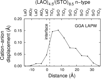
We used the supercell (STO)7.5/(LAO)7.5 for studying the interface electron states, where the half layers in the formula signify an extra layer of TiO2 or LaO, so that we have two identical n-type interfaces (TiO2/LaO) present in the structure. The atomic relaxation was performed using the LAPW method for a slightly different supercell, viz., for (STO)8.5/(LAO)4.5 to keep the calculations manageable. This is reasonable since results presented in Fig. 2 show very little relaxation in the LAO part beyond the second layer, which in turn is consistent with the small charge leakage to the LAO side.
The GGA optimized bulk lattice constants are 3.94 Å and 3.79 Å for the STO and the LAO bulk, respectively, which are quite close to their experimental values (3.905 and 3.789 Å). For the optimization, we fixed the lattice constant for the Sr part to be 3.91 Å, both in the directions parallel and normal to the interface as appropriate for samples grown on the SrTiO3 substrate, while the lattice constant for LAO normal to the interface was chosen to preserve the volume of the bulk unit cell. This defined the supercell which was held fixed, while the internal positions of the atoms were allowed to change in a series of self-consistent calculations until the forces became smaller than about 6 mRy/ au. The main effect of the relaxation, shown in Fig. 2, is to polarize the cation and the anion planes near the interface similar to the relaxation for the well-studied LaTiO3/SrTiO3 interface.popovic ; okamoto1 ; hamann ; popovic-relaxed For the present interface, the atomic polarization occurs mostly in the STO part, with the oxygen atoms moving towards the interface, while the cations move away from it, so that there is a buckling in the planes. The largest cation-anion polarization of about 0.15 Å occurs for the interfacial TiO2 and the SrO layers as seen from Fig. 2.
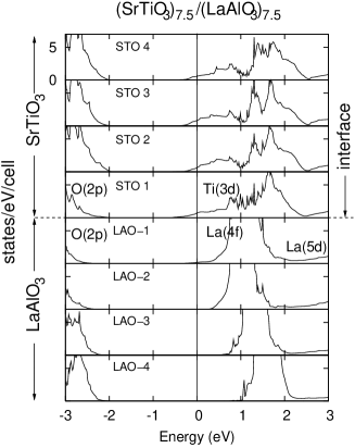
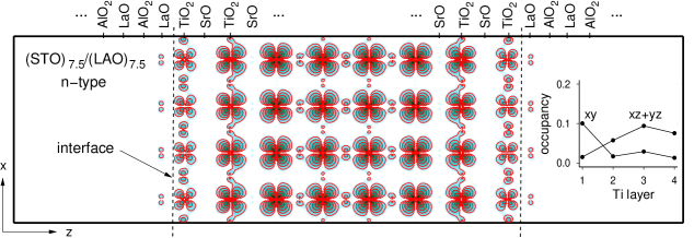
The layer-projected densities-of-states (Fig. 3) calculated with the LMTO method shows that the half electron per unit cell needed to overcome the polar catastrophe resides on the STO side and spreads out to several Ti layers near the interface. The shift of the band edges from layer to layer indicates an electric field discontinuity consistent with the accumulation of a positive monopole charge at the interface. Electrons attracted to this monopole reside on the STO side, as expected from the computed band line-up at the interface (Fig. 4) and confirmed from the charge density contour plot (Fig. 5).

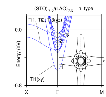
An important result of this work is the existence of two types of carriers at the interface with possibly different transport properties, which is inferred by examining the conduction band structure presented in Fig. 6. The occupied conduction bands are made out of Ti(d) t2g states. As indicated from the wave function characters of Table I, the lowest band is well localized on the first Ti layer because of a much lower interface potential there (Recall that the polar catastrophe argument would place as many as 0.5 electrons per cell at the interface). The xy bands are lower than the yz or zx bands because of the larger hopping integrals along both directions in the xy plane, parallel to the interface. Above these bands at the point are several other bands which occur close together in energy. These are xy-type bands located on the second or the third Ti layer and the yz or xz-type bands, the latter being made out of a linear combination of states on several Ti layers and have small dispersions along one of the two planar directions. Apart from the lowest band, states in the remaining bands spread several layers into the STO part and because of the finite size supercell used in our calculations, the bands belonging to the two interfaces mix, producing a splitting of the energies, visible, e.g., near the X point in the figure. This particular split becomes amplified in the Fermi surface, producing the two outermost wings both along X and Y directions (inset of Fig. 6). The two outermost wings of the Fermi surface would not split without this interaction.
| State | (TiO | (TiO | (TiO | (TiO | rest |
|---|---|---|---|---|---|
| 0.82 | 0.02 | 0 | 0 | 0.16 | |
| 0.02 | 0.17 | 0.44 | 0.26 | 0.11 | |
| 0.01 | 0.35 | 0.18 | 0.37 | 0.09 |
The basic features of the Fermi surface for the isolated interface is illustrated in Fig. 7, which is extracted from the calculated Fermi surface of Fig. 6 and where, for pedagogical reasons, we have omitted the hybridization between the bands. The circles are derived from the xy orbitals, which disperse with the tight-binding matrix element of along both and , resulting in the tight-binding band structure: , which is isotropic for small Bloch momenta, while the xz and the yz orbitals disperse with the tight-binding matrix element along one direction but with a much smallerharrison along the other, so that we have for the xz bands: , and similarly for , which produce the elliptic Fermi surfaces.
Our results suggest a possible explanation for the observed low carrier density for the samples grown under oxygen rich conditions. This growth condition is thought to produce an intrinsic interface, where the observed carrier density is cm-2, corresponding to only about 0.015-0.03 electrons per interface unit cell, much smaller than the half electrons per cell needed to suppress the polar catastrophe. These electrons need not reside on just one interfacial layer, rather, they can be spread over several layers and the polar catastrophe is avoided so long as the total electron count is right. Not all of these electrons might contribute to transport.
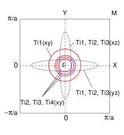
From Fig. 7 we infer the presence of two types of electrons at the interface. The first originates from the lowest conduction subband, which has a strong 2D character consisting mostly of Ti(d) states on the first layer and forming the largest circle in the Femi surface plot. It is well-known that all states in 2D are Anderson localized by disorder and these states may therefore become localized. In addition, these electrons may form self-trapped polarons due to the Jahn-Teller coupling of the Ti(d1) center. The unpaired electron could then behave as a Kondo center. The xz/yz states which form the elliptic Fermi circles in Fig. 7 are also prone to localization on account of their heavy masses along a planar direction. All these electrons may therefore not participate in transport.
The second type of electrons are from the Ti (xy) bands above the lowest band which spread over several Ti layers into the bulk and show up as the three innermost circles in the Fermi surface plot. These electrons have small masses along the plane, they spread several Ti layers into the bulk and are as a result difficult to localize by disorder or electron-phonon coupling and we argue that they are likely the mobile electrons that would contribute to transport in the intrinsic samples. Since the electron density in the Ti(d) bands is low, far from half filling, electron correlation effects are not expected to alter the metallic behavior apart from a mass renormalization in a Fermi liquid picture.
The number of these mobile electrons, estimated from the area of the three innermost circles in Fig. 7 is about cm-2, which is five times smaller than the electrons needed to satisfy the polar catastrophe. It is however still several times higher than the measured carrier density in the intrinsic samples. This discrepancy could be due to several reasons. Density-functional calculations tend to yield too high an energy for localized states, which would mean that the density in the delocalized bands is overestimated. Another possibility is that the mobile carrier density may be reduced due to additional localization effects not considered here explicitly. So, according to this scenario, the mobile electrons arise from the inner pockets in the Fermi surface, while the remaining electrons are localized.
There are indeed signatures of these two types of carriers in the experiments. For instance, Brinkman et al.brinkman were able to explain their transport data in terms of two types of carriers. These experiments showed a Kondo resistance minimum as a function of temperature, which they interpreted in terms of itinerant electrons scattering off of localized Ti (3d) moments. Within our scenario, the formation of the local moments is entirely likely due to the localization of some of the electrons. The delocalized electrons lead to the possibility of superconductivity.reyren
It would be valuable to measure the Hall effect on the intrinsic samples, where several authors have been unsuccessful in observing the Shubnikov-de Haas (SdH) oscillations. It is possible that the oscillations become suppressed due to the intermixing of the localized and the itinerant parts of the Fermi surface, leading to strong scattering between them before the completion of full magnetic orbits. In that case, one might have to go to higher magnetic fields, where magnetic tunneling between the bands might lead to complete orbits.
We thank Jim Eckstein and Michael Ma for insightful discussions and B. R. K. Nanda for help with the computations. ZP and SS would like to acknowledge the hospitality of the Materials Computation Center at the University of Illinois. This work was supported by the U. S. Department of Energy through Grant No. DE-FG02-00ER45818.
References
- (1) Permanent address: INN-“Vinča”, PO Box: 522, 11001 Belgrade, Serbia
- (2) Permanent address: Department of Physics, University of Missouri, Columbia, MO 65211, USA
- (3) A. Ohtomo and H. Y. Hwang, Nature (London) 427, 423 (2004)
- (4) J. N. Eckstein, Nature Materials 6, 473 (2007)
- (5) A. Brinkman et al., Nature Materials 6, 493 (2007)
- (6) W. Siemons et al. Phys. Rev. Lett. 98, 196802 (2007)
- (7) A. Kalabukov et al. Phys. Rev. B 75, 121404 (2007)
- (8) G. Herranz et al., Phys. Rev. Lett. 98, 216 803 (2007)
- (9) S. Thiel et al., Science 313, 1942 (2006)
- (10) W. A. Harrison et al., Phys. Rev. B 18, 4402 (1978); E. A. Kraut, Phys. Rev. B 31, 6875 (1985)
- (11) J. P. Perdew and Y. Wang, Phys. Rev. B 45, 13244 (1992); J. P. Perdew et al., Phys. Rev. Lett. 77, 3865 (1996)
- (12) P. Blaha et al., WIEN2k, An Augmented Plane Wave + Local Orbitals Program for Calculating Crystal Properties (Karlheinz Schwarz, Techn. Universität Wien, Austria), 2001. ISBN 3-9501031-1-2
- (13) O. K. Andersen and O. Jepsen, Phys. Rev. Lett 53, 2571 (1984)
- (14) R. Pentcheva and W. E. Pickett, Phys. Rev. B 74, 035112 (2006)
- (15) M. S. Park, S. H. Rhim, and A. J. Freeman, Phys. Rev. B 74, 205416 (2006)
- (16) J.-M. Albina et al., Phys. Rev. B 76, 165103 (2007)
- (17) C. Cen et al., Nat. Mater. 7, 298 (2008)
- (18) Z. S. Popovic and S. Satpathy, Phys. Rev. Lett. 94, 176805 (2005)
- (19) S. Okamoto, A. J. Millis, and N.A. Spaldin, Phys. Rev. Lett. 97, 056802 (2006)
- (20) D. R. Hamann, D. A. Muller, and H. Y. Hwang, Phys. Rev. B 73, 195403 (2006)
- (21) P. Larson, Z. S. Popovic and S. Satpathy, Phys. Rev. B 77, 245122 (2008)
- (22) J. A. Moland, Phys. Rev. 94, 724 (1954); M. Capizzi and M. Frova, Phys. Rev. Lett. 25, 1298 (1970); S. G. Lim et al., J. Appl. Phys. 91, 4500 (2002); K. van Benthem and C. Elsässer, J. Appl. Phys. 90, 6156 (2001)
- (23) W. A. Harrison, Electronic Structure and the Properties of Solids (Freeman, San Francisco, 1980)
- (24) N. Reyren, et al., Science 317, 1196 (2007)