Perspectives in spintronics: magnetic resonant tunneling, spin-orbit coupling, and GaMnAs
Abstract
Spintronics has attracted wide attention by promising novel functionalities derived from both the electron charge and spin. While branching into new areas and creating new themes over the past years, the principal goals remain the spin and magnetic control of the electrical properties—essentially the I-V characteristics—and vice versa. There are great challenges ahead to meet these goals. One challenge is to find niche applications for ferromagnetic semiconductors, such as GaMnAs. Another is to develop further the science of hybrid ferromagnetic metal/semiconductor heterostructures, as alternatives to all-semiconductor room temperature spintronics. Here we present our representative recent efforts to address such challenges. We show how to make a digital magnetoresistor by combining two magnetic resonant diodes, or how introducing ferromagnetic semiconductors as active regions in resonant tunneling diodes leads to novel effects of digital magnetoresistance and of magnetoelectric current oscillations. We also discuss the phenomenon of tunneling anisotropic magnetoresistance in Fe/GaAs junctions by introducing the concept of the spin-orbit coupling field, as an analog of such fields in all-semiconductor junctions. Finally, we look at fundamental electronic and optical properties of GaMnAs by employing reasonable tight-binding models to study disorder effects.
I Introduction
Spintronics is an interdisciplinary field driven by goals of technological innovations and fundamental discoveries. The two aspects, applied and fundamental, are intimately intertwined, pushing spintronics research forward. Thus far, the only important technological achievements of spintronics remain the giant magnetoresistance and the tunenling magnetoresistance, both based on metallic heterostructures Zutic2004:RMP . While semiconductor spintronics has attracted great deal of attention, most of its device structures are still in the proposal stage, with only few device principles experimentally demonstrated Fabian2007:APS . Moving ahead with realizing potentially useful spintronic devices is a major task.
Spintronics has also generated a great deal of fundamental knowledge. We now have firm understanding of the principles of spin injection, spin transport, and spin relaxation; we have learned how to manipulate spins from bulk to nanoscales, or how to bring ferromagnetism into useful semiconductors Fabian2007:APS . Important, we have learned the limitations of the field, sometimes fundamental in nature, sometimes technology limited.
This article illustrates spintronics perspectives by discussing selected topics, from quantum spintronic devices, through spin-orbit coupling in heterostructures and its implications for tunneling and magnetocrystalline anisotropy, to physical properties of ferromagnetic GaMnAs. There are two important questions that these topics address in their specific forms: (i) What potential spintronic applications can we think of for ferromagnetic semiconductors in general, and for GaMnAs in particular? and (ii) Are hybrid ferromagnetic metal/semiconductor systems a viable alternative to all-semiconductor spintronics? The need to answer the second question stems from the limitations of the physical properties of useful ferromagnetic semiconductors, such as GaMnAs, whose ferromagnetism at room temperature remains elusive.
Where do ferromagnetic semiconductors fit? In most proposals for spintronic devices ferromagnetic semiconductors provide the exchange splitting to differentiate (mainly transport) properties of spin up and spin down electrons. Here we discuss our proposal to take the next step: couple ferromagnetism dynamically with transport and charging, in resonant diodes. We discuss how such a coupling, in the quantum well made of a ferromagnetic semiconductor, leads to robust microwave current oscillations, at nominally dc biases.
One great outcome of spintronics is a good understanding of spin-orbit coupling in semiconductor interfaces. Due to the current limitations on the Curie temperature in GaMnAs, we need to consider conventional sources of spin-polarization: ferromagnetic metals. In particular, ferromagnetic metal/semiconductor interfaces are attractive systems for controlling orbital effects by spins. We discuss here one particular interface, that of Fe/GaAs, and show that tunneling through such junctions leads to the phenomenon of the tunneling magnetoresistance (the tunneling resistance depends on the orientation of the magnetization in the plane perpendicular to the tunneling), which can be explained by the concept of the spin-orbit coupling field at such metal/semiconductor interfaces. Both model and first-principles calculations allow to explore the anisotropies stemming from this interface induced spin-orbit coupling. We also point out that while the transport and magnetocrystalline symmetries both reflect the interface structure, the observed corresponding anisotropies have different electronic origin.
While finding niche applications for GaMnAs is a nontrivial task, the material itself is rather fascinating. It is a highly p-doped semiconductor whose ferromagnetic order is mediated by holes. There are many fundamental questions still open: the Fermi level lies in the valence or in the impurity band? What is the effective mass of the carriers at the Fermi level and what is the mode of the transport? Are the states at the Fermi level fully extended or partially localizes? What is the value of the band gap? and so on. We attempt to answer some of those questions here with two reasonable tight-binding models, finding that each model explains certain experimental features in a complementary way, but neither provides a complete picture; a realistic model of GaMnAs is yet to be presented.
We first introduce magnetic resonant diodes, then discuss tunneling anisotropic magnetoresistance and the spin-orbit coupling effects at ferromagnetic metal/semiconductor interfaces, and finally present our results and their interpretations of our tight-binding calculations of large GaMnAs model systems.
II Magnetic resonant tunneling devices
Spintronic devices aim at enhancing the functionality of the existing electronic technology by exploiting the spin-dependent properties of solid-state systems. An efficient spin control of the charge current would allow for the realization of ultimate magnetoelectric devices, in which information can be processed based on the spin-state of the system Zutic2004:RMP . In this context, band-engineered magnetic semiconductor heterostructures offer promising perspectives, since they provide opportunities for controlling and tuning spin-dependent magneto-transport properties Fabian2007:APS . In particular the rapid development of novel dilute magnetic semiconductors (DMS) in the last decades Ohno1998:S ; Dietl:2007 ; Jungwirth2006:RMP , in which semiconductors are made magnetic by doping with transition metal elements, has considerably enlarged the class of suitable materials for the growing of heterojunction systems.
Magnetic heterostructures typically consist of stacked layers of only a few nanometers of both magnetic and nonmagnetic semiconductors. Along the growth direction the system size becomes comparable to the phase coherence length of the propagating carriers, allowing quantum interference effects to govern the vertical transport properties. According to the band-mismatch of the different semiconductor materials, some of the layers constitute energetic barriers for the incident carriers, which could only be penetrated by tunneling. Nevertheless, in double and multi-barrier systems transmission probabilities up to nearly 100 can be found for certain incident carriers energies, which actually correspond to the discrete electronic spectra of the formed quantum wells; an astonishing effect, termed resonant tunneling.
From a generic point of view, resonant tunneling structures act like an energy filter, allowing only carriers with resonant energies to pass through. The transport becomes strongly sensitive to the relative alignment of the electronic spectra in the leads and the wells, which can be modified by external bias voltages. Even small energy splittings for different spin states in the quantum wells, e.g., induced by an external magnetic field or an exchange field, can result in strong ramifications in the transport characteristics, as has been observed experimentally in paramagnetic Slobodskyy2003:PRL as well as ferromagnetic Ohya2007:PRB ; Oiwa2004:JMMM DMSs quantum well structures. Due to the spin-dependent transmission magnetic resonant tunneling devices have been proposed for realizing efficient spin valve, spin filtering, spin switching, and spin detecting devices Fabian2007:APS ; Petukhov2002:PRL ; Ertler2006a:APL , which form important building blocks for a spin-based information technology.
In the following we show representative examples of capabilities of magnetic heterostructures by describing (i) the digital magneto resistance (DMR), which appears in serially connected resonant tunneling diodes (RTDs), and (ii) the dynamic interplay of transport and magnetic effects in ferromagnetic RTDs, which can lead to selfsustained current oscillations at a nominally steady bias voltage.
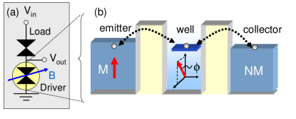
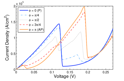
A nice example, which illustrates that the current characteristics can be strongly modified by changing the magnetic properties of resonant tunneling structures, is given by a double barrier structures comprising a ferromagnetic quantum well and a ferromagnetic emitter, as illustrated in Fig. 1(b). Assuming that the magnetization of the quantum well is ”soft“ the relative alignment of the emitter and well magnetization directions can be changed by external magnetic fields. Selfconsistent numerical simulations for GaMnN-like systems Ertler2007a:PRB reveal a strong dependence of the current-voltage (IV) characteristics on the relative magnetization angle, as shown in the lower panel of Fig. 1. In particular, the peak current is considerably decreased if the the well magnetization is tilted away from the parallel alignment with the emitter’s magnetization. This effect can be used to realize the proposed DMR-effect Ertler2006b:APL ; Ertler2007a:PRB in so-called monostable-bistable logic elements (MOBILEs) Maezawa1993:JJAP ; Maezawa:2003 .
A conventional MOBILE consists of two serially connected RTDs, a load and a driver, as shown in Fig. 1(a). The principle of the device operation relies on the nonlinear IV-characteristics of RTDs. By drawing the circuit load line diagram a single monostable output voltage for low input voltages is obtained. However, at high input voltages a bistable working point regime appears. Which of the two working points is realized actually depends on the difference of the load and driver peak currents: if the load peak current is smaller (higher) than the driver’s peak current than the output voltage is low (high). In a nutshell: a MOBILE can compare the peak currents of the load and driver RTDs, yielding a digital binary output signal.
In a magnetic variant of the MOBILE the driver is replaced by a magnetic RTD, e.g, of the kind as discussed above. If the quantum well magnetization is tilted by an external magnetic field the magnetic driver’s peak current is continuously decreased. At some critical angle the driver’s peak current becomes smaller than the load peak current, which results in a discrete jump of the output voltage from low to high. This effectively realizes a digital magneto resistance: the total device resistance makes a discontinuous step by continuously changing the magnetic properties of the structure, i.e, in this case the tilting angle of the quantum well magnetization.
The DMR-like effect has, in fact, already been experimentally demonstrated in a somewhat different device configuration, in which a metallic giant magneto resistance (GMR) element is shunted to a nonmagnetic driver diode Hanbicki2001:APL . In terms of applications DMR-devices could be used as very fast read heads of hard disks, in which the magnetically stored information is directly converted into a binary electrical signal. Furthermore, ferromagnetic RTDs can have the advantage to be nonvolatile upon the loss of power, since the state of the device is stored in the magnetization direction of particular layers of the structure. Such nonvolatile devices are attractive for fast random access memory applications or for reprogrammable logics, in which the logical circuit function is altered by changing the magnetic state of the device.
In addition to magnetically tunable steady state properties, interesting dynamic phenomena can occur in magnetic heterostructures according to a peculiar feedback process, in which the magnetic ordering of the quantum well affects back the resonant tunneling current. In DMSs the ferromagnetic order is mediated by the itinerant carriers, which gives rise to a close interdependence of the transport and magnetic properties. Indeed, several experiments succeeded in generating ferromagnetism by tailoring the carrier density by electrical or optical means Ohno2000:N ; Boukari2002:PRL .
In resonant tunneling structures the particle density in the well strongly depends on the resonant tunneling conditions, which implies that the critical temperature of magnetic quantum wells should be tuneable by external biases, as theoretically predicted in the framework of a mean field model of the well magnetism Lee2002:SST ; Ganguly2005:PRB . These studies revealed that the exchange splitting of the carriers subbands essentially depends (i) on the spin polarization of the particle density in the well and (ii) on the overlap of the subband wave function with the magnetic impurity density profile.
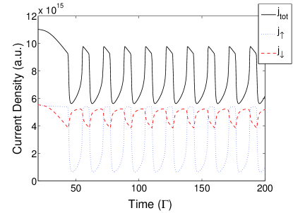
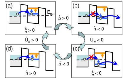
Based on these findings we recently proposed that the combined nonlinear feedback of Coulomb and magnetic interaction can lead to self-sustained high-frequency oscillations of the tunneling current and the quantum well magnetization over a large window of nominally dc-bias voltages Ertler2008:condmat , as illustrated in the upper panel of Fig. 2. The occurrence of these magnetoelectric oscillations needs a built-in energy cut-off of the emitter tunneling rate. This might be realized, e.g, by a cascaded left barrier, which exponentially suppresses the tunneling of carriers with energies smaller than .
A qualitative discussion and explanation for the appearance of the self-sustained oscillations is given in the lower panel of Fig. 2: the electrostatic feedback behaves like an ”inertia“, allowing the spin level with energy to get deeper into the region, in which no carriers can tunnel from the emitter side anymore (), whereas the magnetic feedback is required to push the spin level back into the emitter’s supply region (). The frequency of the oscillations can be modified by the applied dc-bias voltage, which suggest applications of ferromagnetic RTDs as tunable high-power oscillators.
These two examples of magnetic resonant tunneling structures, mainly chosen on the basis of the authors personal research interest, illustrate that magnetic heterostructures have a promising potential for realizing fully integrated magnetoelectronic devices as well as for gaining a deeper understanding of the mechanism of carrier-mediated ferromagnetism. Especially the possibilities of ferromagnetic multi-barrier systems, which naturally provide a rich variety of compositional configurations, are still largely unexplored.
III Tunneling anisotropic magnetoresistance in magnetic junctions
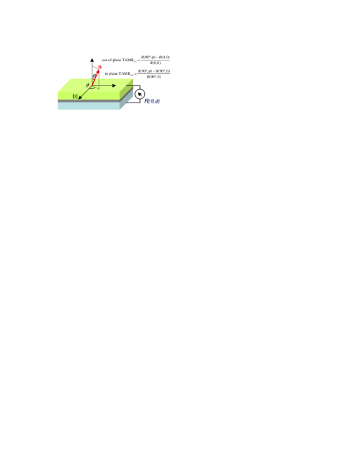
Spin valve devices are layered heterostructures combining ferro- and paramagnetic layers. Such devices are at the heart of the spintronics and are important for the investigation and measurement of spin injection, spin relaxation, and spin polarization. The spin valve devices find also multiple applications in the design of read head sensors and data storage devices, such as magnetic random access memory. The operation of conventional spin valve devices relies on the dependence of the magnetoresistance on the relative orientation of the magnetization in the ferromagnetic leads. The manifestation of such a phenomenon in tri-layer systems composed of two magnetic layers separated by a non-magnetic metallic spacer is called the giant magnetoresistance effect, while in magnetic tunnel junctions (MTJs) composed of an insulating or semiconducting barrier sandwiched between two magnetic electrodes is referred to as the tunneling magnetoresistance (TMR) effect. It has been observed however, that the magnetoresistance in MTJs may also depend on the absolute orientation of the magnetization in the ferromagnetic leads Gould2004:PRL ; Ruster2005:PRL ; Saito2005:PRL ; Brey2004:APL . This phenomenon is called the tunneling anisotropic magnetoresistance (TAMR) effect Gould2004:PRL ; Brey2004:APL . The tunneling magnetoresistance in GaMnAs/GaAlAs/GaMnAs tunnel junctions was theoretically investigated Brey2004:APL . These authors predicted that, as a result of the strong spin-orbit interaction, the tunneling magnetoresistance depends on the angle between the current flow direction and the orientation of the electrode magnetization. Thus, a difference between the tunneling magnetoresistances in the in-plane (i.e., magnetization in the plane of the magnetic layers) and out of plane configurations of up to was predicted for large values of the electrode spin polarization Brey2004:APL . Here we refer to this phenomenon as the out-of-plane TAMR (see Fig. 3). Recent ab initio calculations in Fe/MgO/Fe magnetic tunnel junctions (MTJs) predict an out-of-plane TAMR ratio of about 44 % Khan2008:JPCM . On the other hand, the in-plane TAMR effect refers to the changes in the magnetoresistance when the in-plane magnetization of the ferromagnetic layer(s) is rotated around the direction of the current flow (see Fig. 3).
It is remarkable that the TAMR is present even in MTJs in which only one of the electrodes is magnetic and the conventional TMR is absent. Thus, a new generation of TAMR-based devices could have some advantages with respect to the devices whose operation is based on the TMR effect. In contrast to the conventional TMR-based devices, which require two magnetic layers for their operation, TAMR-based devices can, in principle, operate with a single magnetic lead. Thus the TAMR effect could open new possibilities and functionalities for the operation of spintronic devices. The TAMR effect may have an influence on the spin-injection from a ferromagnet into a non-magnetic semiconductor. Therefore, in order to correctly interpret the results of spin-injection experiments in a spin-valve configuration, it is essential to understand the nature, properties, and origin of the TAMR effect.
The first experimental observation of the TAMR effect was performed in (Ga,Mn)As/AlOx/Au heterojunctions, where an in-plane TAMR ratio of about was found Gould2004:PRL . Experimental investigations of the in-plane TAMR in (Ga,Mn)As/GaAs/(Ga,Mn)As Ruster2005:PRL and (Ga,Mn)As/ZnSe/(Ga,Mn)As Saito2005:PRL tunnel junctions in which both electrodes are ferromagnetic have also been reported. In the case of (Ga,Mn)As/ZnSe/(Ga,Mn)As the in-plane TAMR ratio was found to decrease with increasing temperature, from about at 2 K to at 20 K Saito2005:PRL . This temperature dependence of the in-plane TAMR is more dramatic in the case of (Ga,Mn)As/GaAs/(Ga,Mn)As, for which a TAMR ratio of order of a few hundred percent at 4 K was amplified to at 1.7 K Ruster2005:PRL . This huge amplification of the in-plane TAMR was suggested to originate from the opening of an Efros-Shklovskii gap Efros1975:JPC at the Fermi energy when crossing the metal-insulator transition Ruster2005:PRL . Measurements of the TAMR in (Ga,Mn)As/-GaAs Esaki diode devices has also been reported Ciorga2007:NJP . In addition to the investigations involving vertical tunneling devices the TAMR has also been studied in break junctions Bolotin2006:PRL ; Burton2007:PRB , nanoconstrictions Giddings2005:PRL ; Ciorga2007:NJP and nanocontacts Jacob2008:PRB .
In addition to the currently low Curie temperature ferromagnetic semiconductors, the TAMR has recently been experimentally investigated in Fe/GaAs/Au MTJs Moser2007:PRL , Co/AlOx/Au MTJs Liu2008:NL , and in multilayer-(Co/Pt)/AlOx/Pt structures Park2008:PRL .
In what follows we shall focus our discussion on the case of the in-plane TAMR (for brevity we will refer to it just as the TAMR effect) recently measured in Fe/GaAs/Au MTJs Moser2007:PRL . In such an experiment the magnetization of the ferromagnetic Fe electrode was rotated in-plane by an angle with respect to the [110] crystallographic direction and the magnetoresistance measured as a function of (see Fig. 3). The strength of the TAMR is given by Fabian2007:APS
| (1) |
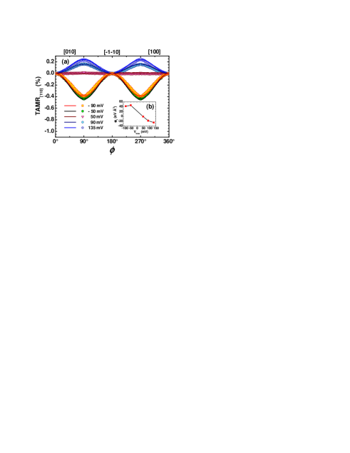
The angular dependence of the TAMR in a Fe/GaAs/Au tunnel heterojunction is shown in Fig. 4(a) for different values of the bias voltage . The symbols represent the experimental data (conveniently mirrored) as deduced from Ref. Moser2007:PRL . Two fundamental features in the behavior of the TAMR can be appreciated in Fig. 4(a): (i) the experimentally measured TAMR exhibits a two-fold symmetry with respect to the magnetization direction in the ferromagnet, (ii) by varying the bias voltage the TAMR can be inverted (i.e., its sign can be changed). In order to explain these experimental findings we have proposed a model (for details see Ref. Fabian2007:APS ) in which the two-fold symmetry of the TAMR in ferromagnet/semiconductor/normal metal junctions emerges from the interference of Dresselhaus and Bychkov-Rashba SOCs. The combined action of these two spin-orbit interactions leads to net, anisotropic SOC with a two-fold symmetry which is compatible with the symmetry of the semiconductor interfaces and manifest in the tunneling magnetoresistance. The Dresselhaus SOC results from the bulk inversion asymmetry of the zinc-blende semiconductor (GaAs in this case) and is characterized by the Dresselhaus parameter which has a finite value in the semiconductor region (for GaAs eV Å2 Fabian2007:APS ) and vanishes elsewhere.
For the small voltages considered in the experiment the main contribution to the Bychkov-Rashba SOC comes from the strong potential gradients at the interfaces rather than from an external electric field. The interface Bychkov-Rashba SOC arises due to the semiconductor interfaces inversion asymmetry Fabian2007:APS and is characterized by the parameters and which measure the strengths of the SOC at the left (ferromagnet/semiconductors) and right (semiconductor/normal metal) interfaces, respectively. These parameters are not known for metal/semiconductor interfaces and have to be extracted from available experimental data Moser2007:PRL or from first-principles calculations (see the following section). For the case of an Fe/GaAs/Au MTJ it turns out that the size of the TAMR is dominated by the parameter corresponding to the ferromagnet/semiconductor interface Fabian2007:APS . Since the values of are irrelevant for the TAMR, one can set this parameter, without loss of generality, to zero. This leaves as a single fitting parameter when comparing to experiment. The theoretical results are shown by solid lines in Fig. 4. The agreement between theory and experiment is very satisfactory. The values of the phenomenological parameter are determined by fitting the theory to the experimental value of the TAMR at . This is enough for the theoretical model to reproduce the complete angular dependence of the TAMR, demonstrating the robustness of the model. By performing the fitting procedure for different values of the bias voltage the bias dependence of can be extracted. The results are shown in Fig. 4(b). The obtained values of have reasonable magnitudes, not too different from known values in semiconductor interfaces Fabian2007:APS . For a bias voltage of about 50 mV the parameter and the TAMR vanishes [compare Figs. 4(a) and (b)]. At a bias slightly bellow 50 mV the interface Bychkov-Rashba parameter changes sign, resulting in the inversion (change of sign) of the TAMR, as seen from Fig. 4(a).
In order to understand the main qualitative behavior of the TAMR, a simplified phenomenological model was proposed in Refs. Moser2007:PRL ; Fabian2007:APS . Such a model is based on a perturbative expansion of the transmissivity in powers of , with denoting the unit vector defining the magnetization direction and being the effective spin-orbit coupling field. Here and represent the average values of the Bychkov-Rashba and linearized Dresselhaus parameters, respectively (note that and ). It was then shown, on the basis of very general symmetry considerations, that up to second order in the strength of the SOC field the angular dependence of the TAMR is determined by the relation (for details see Ref. Fabian2007:APS )
| (2) |
which is consistent with the experimental data and the full theoretical calculations [see Fig. 4(a)]. One can see from Eq. (2) that bias-induced changes of the sign of lead to the inversion of the TAMR. It is also clear that when , the TAMR is suppressed. Therefore, for a finite in-plane TAMR both Bychkov-Rashba and Dresselhaus SOCs must necessarily be present. This is in contrast to the case of the TAMR in the out-of-plane configuration for which the presence of only Bychkov-Rashba coupling suffices Brey2004:APL ; Chantis2007:PRL ; Khan2008:JPCM .
IV Ab-Initio study of spin-orbit coupling effects in Fe/GaAs interfaces
The spin-orbit interaction couples electron spin to the orbital moment. In magnetic systems the spin-orbit interaction is the primary source of the magnetocrystalline anisotropy. In Fe films grown on semiconductors with a cubic zinc-blende structure, e.g., ZnSe, GaAs or InAs, a uniaxial magnetic anisotropy has been reported Krebs1987:JAP . This comes rather as a surprise since both the Fe and the semiconductors have cubic symmetry. The easy axis has been found along or directions. The origin of the different easy axis orientations has been attributed to the different semiconductor surface reconstructions. Kneedler et al. Kneedler1997:PRB showed that strain in the Fe film grown on GaAs(001) surface has negligible effect on the easy axis orientation indicating that it is independent of the surface reconstruction. Moosbühler et al. Moosbuehler2002:JAP investigated and surface reconstructions and pointed out that easy axis is always along with practically the same amplitude for different Fe film thicknesses. It is of importance to introduce a realistic model for the origin of the uniaxial magnetic anisotropy as well as to relate it to the TAMR effect, whose bias induced reversal is well described, on the one hand, by the interference between Bychkov-Rashba and Dresselhaus spin-orbit couplings Fabian2007:APS ; Moser2007:PRL and, on the other hand, by the reversal of the spin polarization Chantis2007:PRL99 . The interface structure also affects the Schottky barrier height Demchenko2006:PRB and consequently spin injection to the GaAs.
As the lattice constant of the bulk GaAs () is almost twice the lattice constant of the bcc Fe (), the smooth epitaxial growth of Fe on a GaAs(001) surface is possible Krebs1987:JAP ; Brockmann1999:JMMM . Erwin et al. Erwin2002:PRB studied, using density functional theory, the stability of ideal Fe/GaAs interfaces. Their study revealed that the thickness of the Fe film as well as the type of the GaAs surface termination (As- or Ga-like) affects the interface stability. Three types of Fe/GaAs interface models have been investigated Erwin2002:PRB : (i) model A - flat interface [Fig.5(a)]; (ii) model B - partially intermixed interface [Fig.5(b)]; (iii) model C - fully intermixed interface [Fig.5(c)]. When more than two atomic layers of Fe are deposited on a GaAs(001) surface, the flat (model A) and partially intermixed (model B) interface models are more stable than the fully intermixed ones (model C). As the hybridization lowers the cohesive energy Mirbt2003:PRB , the antibonding bonds between Fe and As are more stable than the Fe-Ga bonds. Interestingly, while the density functional calculations imply that the As-terminated flat (model A) interface is more stable then the partially intermixed (model B) Erwin2002:PRB one, a recent Z-contrast scanning transmission electron microscopy experiment reported a single plane of alternating Fe and As atoms (model B) in an Fe/AlGaAs interface Zega2006:PRL .
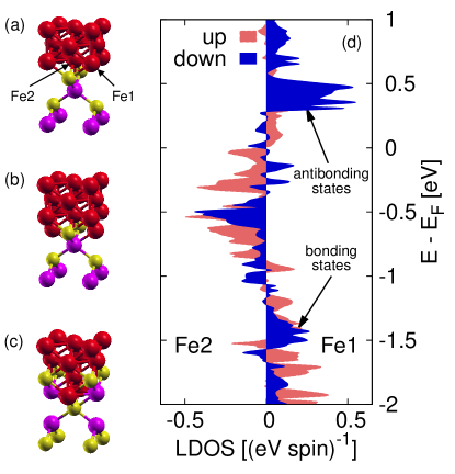
In the following we discuss electronic properties of an ideal slab structure of the flat interface model (model A) between Fe and As-terminated GaAs(001). The slab encased in vacuum of the thickness contains 9 atomic planes of GaAs and three atomic planes of bcc Fe on top of the GaAs(001) surface. The orthorombic symmetry of the system is reduced due to the spin-orbit coupling, depending on the orientation of the magnetization in the Fe. The presence of the much debated uniaxial magnetic anisotropy can be explained in this flat interface model by means of directional covalent bonds at the interface Sjostedt2002:PRL . The interface breaks the natural continuation of the tetrahedral bonds of the zinc-blende structure. Because of that, in what follows two inequivalent groups of Fe atoms at the interface can be distinguished. The first group contains Fe atoms Fe1 [see Fig.5(a)], which are in ”bonding” positions, e.g., the sites where Ga atoms would have been situated. The second group contains Fe2 atoms that correspond to voids in a zinc-blende structure. These nonequivalent Fe atoms show similar local densities of states (LDOS), but if one plots the difference of the -projected LDOS, see Fig.5(d), the coupling of the Fe film to the GaAs substrate appears to be clear. The -states about 0.5 eV below the Fermi level () are split in the case of Fe1 due to bonds between hybridized states (As) and -states (Fe1) to bonding (1.4 eV bellow ) and antibonding states (0.4 eV above ). Thus, by means of LDOS one finds the answer that uniaxial magnetocrystalline anisotropy has its origin in anisotropic interfacial bonds Sjostedt2002:PRL , which represents a microscopic mechanism causing the magnetic anisotropy in the Fe/GaAs heterostructure. It has been shown in case of Zn-terminated Fe/ZnSe(001) system that all Fe atoms in ”bonding” positions contribute to uniaxial magnetic anisotropy with easy axis along direction while atoms in void-like positions along direction with 40-times lower magnitude Sjostedt2002:PRL . In the case of Se-terminated interface the easy axis points along . In the case of Fe/GaAs heterostructure one assumes similar trends since the splitting of the bonding states is analogous.
In addition to the magnetic anisotropy, a novel transport phenomenon has been discovered in Fe/GaAs heterostructures: a tunneling anisotropic magnetoresistance (TAMR) effect, as discussed in the previous section. This effect, which has been observed in Fe/GaAs/Au junctions Moser2007:PRL with epitaxial Fe/GaAs interfaces, has challenged our understanding of ferromagnetic metal/semiconductor junctions. Indeed, a typical spin-valve like behavior has been observed for a junction that contains only a single ferromagnetic layer; at least two layers are needed for conventional spin valve phenomena. To investigate the origin of the TAMR effect have proposed a simplified model of a ferromagnet/semiconductor heterostructure based on general symmetry considerations Moser2007:PRL ; Fabian2007:APS . The spin-orbit coupling in the junction is manifested through linear (in momentum) Bychkov-Rashba and Dresselhaus terms, which reflect, respectively, the structure and bulk inversion asymmetry of the Fe/GaAs heterostructure. Interference of these spin-orbit couplings leads in [001] quantum wells to the symmetry. The same symmetry then appears in the tunneling magnetoresistance, which is a function of the magnetization direction Moser2007:PRL . In addition, we consider a spin splitting, which describes the splitting of the corresponding spin states due to the strong exchange splitting in the Fe film. The eigenspectrum, in the limit of a strong exchange splitting (well justified since the splitting in Fe is about 1.5 eV, much more than the splitting due to the spin-orbit interaction) close to the Brillouin zone center is
| (3) |
Since we have allowed for band dependent Bychkov-Rashba () and Dresselhaus () parameters, we can identify the effect of the spin-orbit coupling on the parabolic band as a shift that depends on the spin (), the sign of and , the orientation of the magnetization () as well as the orientation of the momentum (). Performing a fitting of ab-initio data to the eigenspectrum Eq.(3) we have obtained effective Bychkov-Rashba and Dresselhaus parameters. We have found that the Bychkov-Rashba parameters change sign within the energy window of about 250 meV above and below . Since the sign of TAMR depends on the product [see Eq.(2)] we can conclude that the bias induced TAMR reversal, observed in Ref. Moser2007:PRL , can be explained by the change of the sign of the Bychkov-Rashba parameters.
It would be reasonable to expect that the magnetocrystalline anisotropy can be influenced by an applied bias in the same way as the tunneling anisotropic magnetoresistance. As we have seen, though, the two effects originate from different electronic states: magnetocrystalline anisotropy is given by the states deep below the Fermi level, while TAMR is determined by the propagating states close to the Fermi level. The bias dependence of the TAMR means that states within a transport window (given by the bias) contribute. As these states have in principle different spin-orbit field parameters, upon averaging over the transport window we obtain different resistance at different biases; we are probing different states. Such an averaging would not change the magnetocrystalline anisotropy which is dominated by the spin-orbit effects of the deep lying states. However, one could expect effects due to the bias dependent electronic deformation of these states.
V Tight-binding modeling of electronic and optical properties of GaMnAs
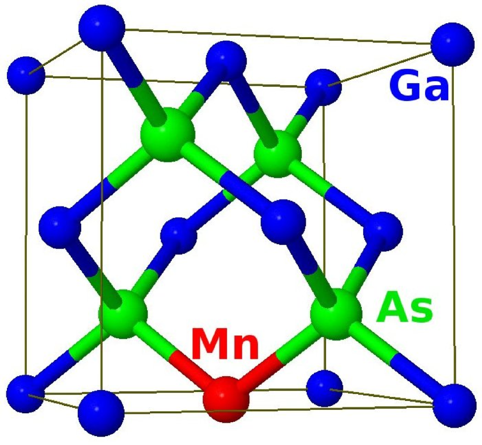
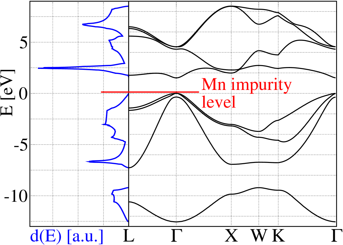
Diluted magnetic semiconductors have been subject to very active research during the past years due to their promising role for new spin-electronic devices Fabian2007:APS . GaMnAs is a much studied material system among these magnetic semiconductors as its Curie temperature is rather high, reaching about 170 K Ohno1998:S ; Jungwirth2006:RMP . The host material, GaAs, is a III-V fcc semiconductor with a band gap of eV; the Mn impurity has a binding energy of eV when it replaces a Ga atom, see Fig. 6. Since Mn is short one electron compared with Ga at the valence levels, substitutional Mn impurities act as acceptors that carry a local magnetic moment leading to a hole mediated ferromagnetism MacDonald05 .
Despite efforts to understand the bulk properties of ferromagnetic GaMnAs both from an experimental and theoretical point of view a number of questions remain open. It is still an unsettled issue whether the free carriers (holes) reside in an impurity band which is detached from the host valence band or in the valence band itself. To this end various absorption experiments Nagai01 ; Hirakawa02 ; Burch06a were performed. However, the Mn concentration threshold for which the impurity band, that appears for very low Mn concentrations, eventually merges with the host valence band could not uniquely be determined. Measurements of the Fermi energy in GaMnAs and the size of the gap as a function of the impurity concentration are presented in Tsuruoka02 ; Thomas07 . These characteristics are important for the design and study of spintronic devices as well as for spin injection experiments. Further open questions concern the scattering and localization properties of the holes caused by the disorder in the material. Besides the impurity band picture Burch06a , an interpretation based on a merged impurity and valence band together with the existence of localized states in the band tail could also explain the absorption experiments Jungwirth07a . A wide range of theoretical models describing the electronic properties of GaMnAs has been reviewed in Jungwirth2006:RMP . Among these are first-principles calculations Sandratskii04 ; Stroppa08 , effective single particle tight-binding approaches Tang04a ; Dorpe05 ; Sankowski06 ; Masek07a , tight-binding approaches in combination with percolation theory Bhatt02 ; Kaminski02 ; DasSarma03 , dynamical mean field theories Majidi06 , effective theories based on Hamiltonians Dietl00 ; Dietl01 ; Yang03 ; Elsen07 , and large-scale Monte-Carlo studies of a real space Hamiltonian Yildrim07a .
In our studies we address these open questions using a phenomenological multi-band tight-binding simulation method for ferromagnetic bulk GaMnAs. This material specific method treats the Mn impurities in a non-perturbative way and can be applied to system sizes of up to 2000 atoms (nowadays) with reasonable computational effort. It is based on well-known tight-binding models for the host GaAs material which include spin orbit coupling Chadi77a ; Talwar82a . The disorder effects are modeled by changing the on-site and hopping terms of those Ga sites that are replaced by the Mn impurities. We compare two recent proposals, one due to Mašek and the other due to Tang and Flatté. The first approach is based on a second-nearest neighbor approximation for the host GaAs Talwar82a and determines the Mn tight-binding parameters by means of first principles calculations in a Mn concentration regime around % Masek07a ; Masek07b . The second approach remains within the nearest neighbor approximation Chadi77a . It is based on a fit of two physically relevant tight-binding parameters to reproduce the binding energy of a single Mn impurity in the GaAs host material Tang04a ; Kitchen06a . In either case an effective single-particle model is obtained which treats the carrier-carrier interactions in a mean field approximation.
As it is not clear yet which of the two different parameter sets (if any) is better suited for the description of available experimental data we have investigated the density of states, the position of the Fermi energy, the size of the gap, the localization properties of the wavefunctions and the optical conductivity of GaMnAs for both models and compared the results to experimental findings Turek08a .
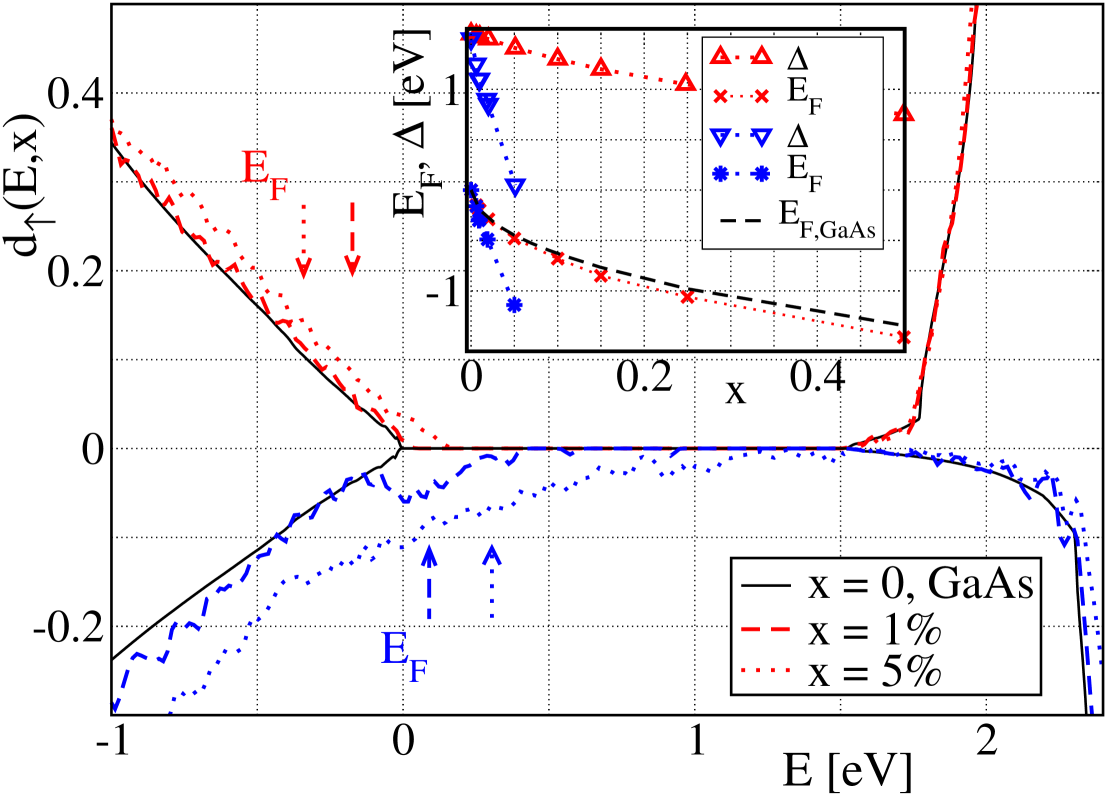
First, we present the results of both models for the density of states in the dependence on the Mn concentration . In Fig. 7 the density is shown for the spin up states only as the spin down contributions follow the GaAs density very closely. Because the two models are based on different parameter sets for clean GaAs the resulting densities also show a slightly different behavior, in particular for the conduction band.
Photoconductivity experimentsThomas07 on GaMnAs heterostructures yield a gap eV for % with being close to the impurity level. Scanning tunneling microscopy measurements Tsuruoka02 resulted in eV for a similar concentration. However, a quantitative comparison with the experimental data and our results is not possible due to the uncertainty in the number of Mn interstitials in the experimental data.
For Mašek’s model the density of states shows only minor modifications due to the increasing disorder, see Fig. 7. There is no detached impurity band forming in the relevant range of Mn concentrations . The Fermi energy decreases into the host valence band as the Mn impurities increase the number of holes. If the Fermi energy is measured from the top of the GaMnAs valence band as a function of the Mn impurity one finds a close similarity to clean p-GaAs with the corresponding number of holes added, see inset of Fig. 7. For the second model due to Tang and Flatté the situation is completely different. An impurity band, which merges with the host valence band at Mn concentrations % can clearly be identified, see lower curves of Fig. 7. A large number of valence states are shifted into the host gap resulting in a Fermi energy which increases compared to the top of the host valence band. The gap eventually disappears at %; this is not consistent with experiment.
Besides the density of states, the localization properties of the states around the Fermi energy play an important role for transport phenomena. We studied these properties by means of the participation ratio and found that the states around the Fermi energy are extended in both models. Similar analysis for energies closer to the band edge leads to a different result for the model by Tang and Flatté. At these higher energies in the GaMnAs valence band tail one finds strongly localized states Turek08a .
The optical conductivity is closely related to the absorption and can be directly accessed in experimentsBurch06a ; Katsumoto01 ; Hirakawa02 . However, there are still some discrepancies in the results and the interpretation of the data concerning the low frequency limit, the position of the intervalence band peaks, and the deduced effective masses and mean free paths. The two different models we studied result in two qualitatively different line shapes for . Mašek’s model shows a Drude peak at zero frequency while no such peak is observed in Tang and Flatté’s model. However, despite all the qualitative differences of the two models, i.e. concerning the existence of an impurity band, the calculated effective masses are similar being within the range of – of the free electron mass.
We conclude that phenomenological tight-binding methods are well suited for the simulation of material properties of ferromagnetic semiconductors as they include the disorder in a non-perturbative way. However, neither of the two proposed parameterizations studied by us describes satisfactorily available experimental data. They both describe some properties correctly while failing at others.
References
References
- (1) Žutić I, Fabian J and Das Sarma S 2004 Rev. Mod. Phys. 76 323–410
- (2) Fabian J, Matos-Abiague A, Ertler C, Stano P and Žutić 2007 Acta Phys. Slov. 57 565–907
- (3) Ohno H 1998 Science 281 951–956
- (4) Dietl T 2007 in W Pötz, J Fabian and U Hohenester, eds, Modern Aspects of Spin Physics (Springer, Berlin) pp 1–46
- (5) Jungwirth T, Sinova J, Mašek J, Kučera J and MacDonald A H 2006 Rev. Mod. Phys. 78 809–864
- (6) Slobodskyy A, Gould C, Slobodskyy T, Becker C R, Schmidt G and Molenkamp L W 2003 Phys. Rev. Lett. 90 246601
- (7) Ohya S, Hai P N, Mizuno Y and Tanaka M 2007 Phys. Rev. B 75 155328–1–155328–6
- (8) Oiwa A, Moriya R, Kashimura Y and Munekata H 2004 J. Magn. Magn. Mater. 272-276 2016–2017
- (9) Petukhov A G, Chantis A N and Demchenko D O 2002 Phys. Rev. Lett. 89 107205
- (10) Ertler C and Fabian J 2006 Appl. Phys. Lett. 89 242101–1–242101–3
- (11) Ertler C and Fabian J 2007 Phys. Rev. B 75 195323–1–195323–9
- (12) Ertler C and Fabian J 2006 Appl. Phys. Lett. 89 193507–1–193507–3
- (13) Maezawa K and Mizutani T 1993 Jpn. J. Appl. Phys. 32 L42–L44
- (14) Maezawa K and Förster A 2003 in R Waser, ed, Nanoelectronics and Information Technology (Wiley-VCH, Weinheim) pp 407–424
- (15) Hanbicki A T, Mango R, Cheng S F, Park Y D, Bracker A S and Jonker B T 2001 Appl. Phys. Lett. 79 1190–1192
- (16) Ohno H, Chiba D, Matsukura F, Abe T O E, Dietl T, Ohno Y and Ohtani K 2000 Nature 408 944–946
- (17) Boukari H, Kossacki P, Bertolini M, Ferrand D, Cibert J, Tatarenko S, Wasiela A, Gaj J A and Dietl T 2002 Phys. Rev. Lett. 88 207204
- (18) Lee B, Jungwirth T and MacDonald A H 2002 Semi. Sci. Techn. 17 393–403
- (19) Ganguly S, Register L F, Banerjee S and MacDonald A H 2005 Phys. Rev. B 71 245306–1–245306–8
- (20) Ertler C and Fabian J 2008 Phys. Rev. Lett. 101 077202
- (21) Gould C, Rüster C, Jungwirth T, Girgis E, Schott G M, Giraud R, Brunner K, Schmidt G and Molenkamp L W 2004 Phys. Rev. Lett. 93 117203
- (22) Rüster C, Gould C, Jungwirth T, Sinova J, Schott G M, Giraud R, Brunner K, Schmidt G and Molenkamp L W 2005 Phys. Rev. Lett. 94 027203
- (23) Saito H, Yuasa S and Ando K 2005 Phys. Rev. Lett. 95 086604
- (24) Brey L, Tejedor C and Fernández-Rossier J 2004 Appl. Phys. Lett. 85 1996–1998
- (25) Khan M N, Henk J and Bruno P 2008 J. Phys. Condens. Matter 20 155208
- (26) Efros A L and Shklovskii B I 1975 J. Phys. C 8 L49–L51
- (27) Ciorga M, Schlapps M, Einwanger A, Geißler S, Sadowski J, Wegscheider W and Weiss D 2007 New J. Phys. 9 351
- (28) Bolotin K I, Kuemmeth F and Ralph D C 2006 Phys. Rev. Lett. 97 127202
- (29) Burton J D, Sabrinov R F, Velev J P, Mryasov O N and Tsymball E Y 2007 Phys. Rev. B 76 144430
- (30) Giddings A D, Khalid M N, Jungwirth T, Wunderlich J, Yasin S, Edmonds R P C K W, Sinova J, Ito K, K-Y Wang, Williams D, Gallagher B L and Foxon C T 2005 Phys. Rev. Lett. 94 127202
- (31) Jacob D, Fernández-Rossier J and Palacios J J 2008 Phys. Rev. B 77 165412
- (32) Moser J, Matos-Abiague A, Schuh D, Wegscheider W, Fabian J and Weiss D 2007 Phys. Rev. Lett. 99 056601
- (33) Liu R S, Michalak L, Canali C M, Samuelson L and Pettersson H 2008 Nano Lett. 8 848–852
- (34) Park B G, Wunderlich J, Williams D A, Joo S J, Jung K Y, Shin K H, Olejník K, Schik A B and Jungwirth T 2008 Phys. Rev. Lett. 100 087204
- (35) Chantis A N, Belashchenko K D, Tsymbal E Y and van Schilfgaarde M 2007 Phys. Rev. Lett. 98 046601
- (36) Krebs J J, Jonker B T and Prinz G A 1987 J. Appl. Phys. 61 3744
- (37) Kneedler E M, Jonker B T, Thibado P M, Wagner R J, Shanabrook B V and Whitman L J 1997 Phys. Rev. B 56 8163 – 8168
- (38) Moosbühler R, Bensch F, Dumm M and Bayreuther G 2002 J. Appl. Phys. 91 8757
- (39) Chantis A N, Belashchenko K D, Smith D L, Tsymbal E Y, van Schilfgaarde M and Albers R C 2007 Phys. Rev. Lett. 99 196603
- (40) Demchenko D O and Liu A Y 2006 Phys. Rev. B 73 115332
- (41) Brockmann M, Zölfl M, Miethaner M and Bayreuther G 1999 J. Magn. Magn. Mater. 198 384
- (42) Erwin S C, Lee S and Scheffler M 2002 Phys. Rev. B 65 205422
- (43) Mirbt S, Sanyal B, Isheden C and Johansson B 2003 Phys. Rev. B 67 155421
- (44) Zega T J, Hanbicki A T, Erwin S C, Žutić I, Kioseoglou G, Li C H, Jonker B T and Stroud R M 2006 Phys. Rev. Lett. 96 196101
- (45) Sjöstedt E, L Nordström F G and Eriksson O 2002 Phys. Rev. Lett. 89 267203
- (46) MacDonald A H, Schiffer P and Samarth N 2005 Nat. Mat. 4 195
- (47) Nagai Y, Kunimoto T, Nagasaka K, Nojiri H, Motokawa M, Matsukura F, Dietl T and Ohno H 2001 Jpn. J. Appl. Phys. 40 6231
- (48) Hirakawa K, Katsumoto S, Hayashi T, Hashimoto Y and Iye Y 2002 Phys. Rev. B 65 193312
- (49) Burch K S, Shrekenhamer D B, Singley E J, Stephens J, Sheu B L, Kawakami R K, Schiffer P, Samarth N, Awschalom D D and Basov D N 2006 Phys. Rev. Lett. 97 087208
- (50) Tsuruoka T, Tachikawa N, Ushioda S, Matsukura F, Takamura K and Ohno H 2002 Applied Physics Letters 81(15) 2800–2802
- (51) Thomas O, Makarovsky O, Patanè A, Eaves L, Campion R P, Edmonds K W, Foxon C T and Gallagher B L 2007 Applied Physics Letters 90(8) 082106
- (52) Jungwirth T, Sinova J, MacDonald A H, Gallagher B L, Novak V, Edmonds K W, Rushforth A W, Campion R P, Foxon C T, Eaves L, Olejn’ik K, Masek J, Yang S R E, Wunderlich J, Gould C, Molenkamp L W, Dietl T and Ohno H 2007 Phys. Rev. B 76 125206
- (53) Sandratskii L M, Bruno P and Kudrnovský J 2004 Phys. Rev. B 69 195203
- (54) Stroppa A, Picozzi S, Continenza A, Kim M Y and Freeman A J 2008 Phys. Rev. B 77(3) 035208
- (55) Tang J M and Flatté M E 2004 Phys. Rev. Lett. 92 047201
- (56) VanDorpe P, VanRoy W, DeBoeck J, Borghs G, Sankowski P, Kacman P, Majewski J A and Dietl T 2005 Phys. Rev. B 72(20) 205322
- (57) Sankowski P, Kacman P, Majewski J and Dietl T 2006 Physica E 32 375
- (58) Mašek J 2007 private communication
- (59) Bhatt R, Berciu M, Kennett M P and Wan X 2002 Journal of Superconductivity: INM 15 71
- (60) Kaminski A and DasSarma S 2002 Phys. Rev. Lett. 88 247202
- (61) DasSarma S, Hwang E H and Kaminski A 2003 Phys. Rev. B 67 155201
- (62) Majidi M A, Moreno J, Jarrell M, Fishman R S and Aryanpour K 2006 Phys. Rev. B 74(11) 115205
- (63) Dietl T, Ohno H, Matsukura F, Cibert J and Ferrand D 2000 Science 287 1019
- (64) Dietl T, Ohno H and Matsukura F 2001 Phys. Rev. B 63 195205
- (65) Yang S R E, Sinova J, Jungwirth T, Shim Y P and MacDonald A H 2003 Phys. Rev. B 67 045205
- (66) Elsen M, Jaffres H, Mattana R, Tran M, George J M, Miard A and Lemaitre A 2007 Phys. Rev. Lett. 99(12) 127203
- (67) Yildirim Y, Alvarez G, Moreo A and Dagotto E 2007 Phys. Rev. Lett. 99 057207
- (68) Chadi D J 1977 Phys. Rev. B 16 790
- (69) Talwar D N and Ting C S 1982 Phys. Rev. B 25 2660
- (70) Mašek J, Kudrnovský J, Máca F, Sinova J, MacDonald A H, Campion R P, Gallagher B L and Jungwirth T 2007 Phys. Rev. B 75 045202
- (71) Kitchen D, Richardella A, Tang J M, Flatté M and Yazdani A 2006 Nature 442 436
- (72) Turek M, Siewert J and Fabian J 2008 Phys. Rev. B 78 085211
- (73) Katsumoto S, Hayashi T, Hashimoto Y, Iye Y, Ishiwata Y, Watanabe M, Eguchi R, Takeuchi T, Harada Y, Shin S and Hirakawa K 2001 Mater. Sci. Eng. B 84 88